
Zixin Liang, Yuanyuan Zhao, Xuanming Duan. Principle and Technology of Laser Super-Diffraction Lithography[J]. Laser & Optoelectronics Progress, 2022, 59(9): 0922029
- Laser & Optoelectronics Progress
- Vol. 59, Issue 9, 0922029 (2022)
![Schematic diagram of molecular states in microscopic imaging and lithography[21]](/richHtml/lop/2022/59/9/0922029/img_01.jpg)
Fig. 1. Schematic diagram of molecular states in microscopic imaging and lithography[21]
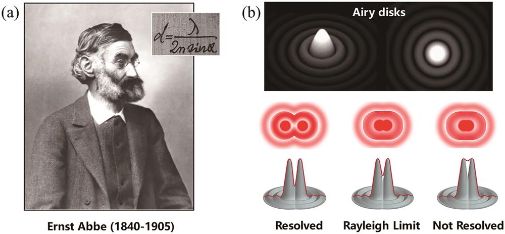
Fig. 2. Determination of diffraction limit. (a) Abbe and Abbe diffraction limit formula; (b) diffraction limit based on Rayleigh criterion
Fig. 3. Index of lithographic resolution[59]
Fig. 4. Super-diffraction lithography based on near-field tip enhancement technique. (a) (b) Near-field tip opening photolithography and 24 nm super-diffraction polymerization lines[63]; (c) (d) near-field tip enhancement lithography diagram and local enhancement simulation diagram [62]; (e) grating structures with 70 nm line width, 70 nm spacing, and 140 nm period under near-field tip enhanced lithography [62]
Fig. 5. Super-diffraction lithography based on SPP. (a) Diagram of SPP lithography[15]; (b) 60 nm half-spaced dense lines fabricated in a plasma chamber with high spatial spectral OAI [14]; (c) combination of bow-knot aperture structure and plasma cavity near-field super-diffraction[77]
Fig. 6. Super-resolution imaging and super-diffraction lithography based on the principle of spherical focusing. (a) Experimental configurations of white microspheres with λ/8—λ/14 imaging resolution[61]; (b) (c) super-resolution imaging of 130 nm line spacing and 50 nm diameter holes obtained by using microsphere lens imaging[61]; (d) distribution of the light field when the ball is focused in the photoresist[80]; (e) nanodot array patterns generated by spherical focus lithography[80]
Fig. 7. Super resolution imaging based on super oscillation phenomenon. (a)(b) Super-oscillation phenomenon super-resolution principle[84-85]; (c) SEM image and imaging focal spot calculation simulation and actual system diagram of superoscillating lens[86]; (d)-(g) 121 nm slits were superresolved by a superoscillating lens[86]; (h) indiscernible slits under conventional objective lens NA=1.4[86]
Fig. 8. Resolution enhancement principle based on multiphoton absorption effect. (a) Sub-diffraction limit processing accuracy diagram (dotted line is single-photon absorption probability, solid line is two-photon absorption probability, and illustration is diffraction pattern of optical devices)[94]; (b) removal of "blury" by multi-photon absorption[20]; (c)-(e) photolithographic lines SEM images of multi-photon absorption in different modes (910 nm, 780 nm, and 650 nm)
Fig. 9. Super-diffraction photolithography principle based on STED. (a) Principle of double beam super-resolution machining[93]; (b) dual-beam single-photon STED processing schematic diagram and 64 nm half-height full-width line SEM diagram[96]
Fig. 10. Laser direct writing super-diffraction lithography based on two-photon polymerization principle. (a) "Microbull” prepared by two-photon polymerization; (b)-(d) polymer under different processing conditions and two-photon absorption probability under different laser pulse energies; (e)-(f) spring vibrator with diameter of 300 nm prepared by two-photon polymerization (scale bars: 2 μm)[22]
Fig. 11. Resolution of laser direct writing two-photon super-diffraction lithography. (a) Minimum line width of 100 nm nanowires on the glass substrate [101]; (b) minimum line width of 80 nm nanowires on the glass substrate and the molecular structure of the used initiator and crosslinking agent [103]; (c) 50 nm nanowires on glass substrate [104]; (d) 35nm nanowires on the glass substrate[105];(e)-(g)fabrication of suspension line structures with minimum feature sizes of 30 nm [106], 18 nm [107], and 7 nm [108]
Fig. 12. Laser direct writing super-diffraction lithography based on STED principle. (a) Schematic experimental apparatus for fast lithography using pulse excitation beam and phase continuous wave inactivation beam[37]; (b) (c) 40 nm polymer lines obtained by SETD direct write lithography[37]; (d) (e) comparison of polymers under different absorption mechanisms[37]; (f)-(k) 9 nm suspended lines prepared by STED direct writing technique[122]
Fig. 13. Method of laser direct writing process based on photothermal phase transformation principle for 5 nm gap fabrication[129]. (a) Fabrication of nanoslits by overlapping two laser beams; (b) simulation results of laser irradiation on the heating distribution of the two-layer Ti/SiO2 structure; (c) AFM image of slit width varying with laser power; (d) calculation of oxidation depth under different conditions and slit SEM images
Fig. 14. Super-diffraction projection lithography system and fabricated patterns. (a) DMD projection lithography system based on 405 nm LED light source[142]; (b) SEM photograph of µNOEL Logos lithographic pattern (minimum critical dimension is 180 nm)[142]
Fig. 15. Multi-focus scanning two-photon lithography based on DMD. (a) Multi-focus scanning two-photon polymerization lithography system; (b) single focus, double focus, and multi-focus scanning process; (c) 500 nm suspended lines from DMD multi-focus scanning lithography[139]
Fig. 16. Femtosecond laser two-photon projection lithography based on spatial and temporal focusing. (a) Schematic diagram of nano-lithography based on space-time focusing technology; (b) polymers with transverse widths of 139-140 nm and axial linewidths of 175 nm fabricated by spatio-temporal focusing techniques [143]
Fig. 17. Multiphoton lithography using spatiotemporal focusing. (a) Multi-photon photolithography combined with space-time focusing projection photolithography system optical path diagram; (b) printing of suspended line structures with Z-axis compression under spatiotemporal focusing technology (minimum height of suspended line is 1 μm)[144]
Fig. 18. Femtosecond laser two-photon maskless projection super-diffraction nanolithography[38]. (a) DMD projection nanolithography system based on 400 nm femtosecond laser; (b) SEM image of polymer lines with a minimum width of 32 nm; (c) SEM images of microcircuit patterns with multiscale controllable feature sizes including the equal line width of 150 nm

Set citation alerts for the article
Please enter your email address
© Copyright 2018-2021 | Chinese Laser Press. All Rights Reserved 沪ICP备15018463号-20