Xuhan Guo, An He, Yikai Su. Recent advances of heterogeneously integrated III–V laser on Si[J]. Journal of Semiconductors, 2019, 40(10): 101304
Search by keywords or author
- Journal of Semiconductors
- Vol. 40, Issue 10, 101304 (2019)
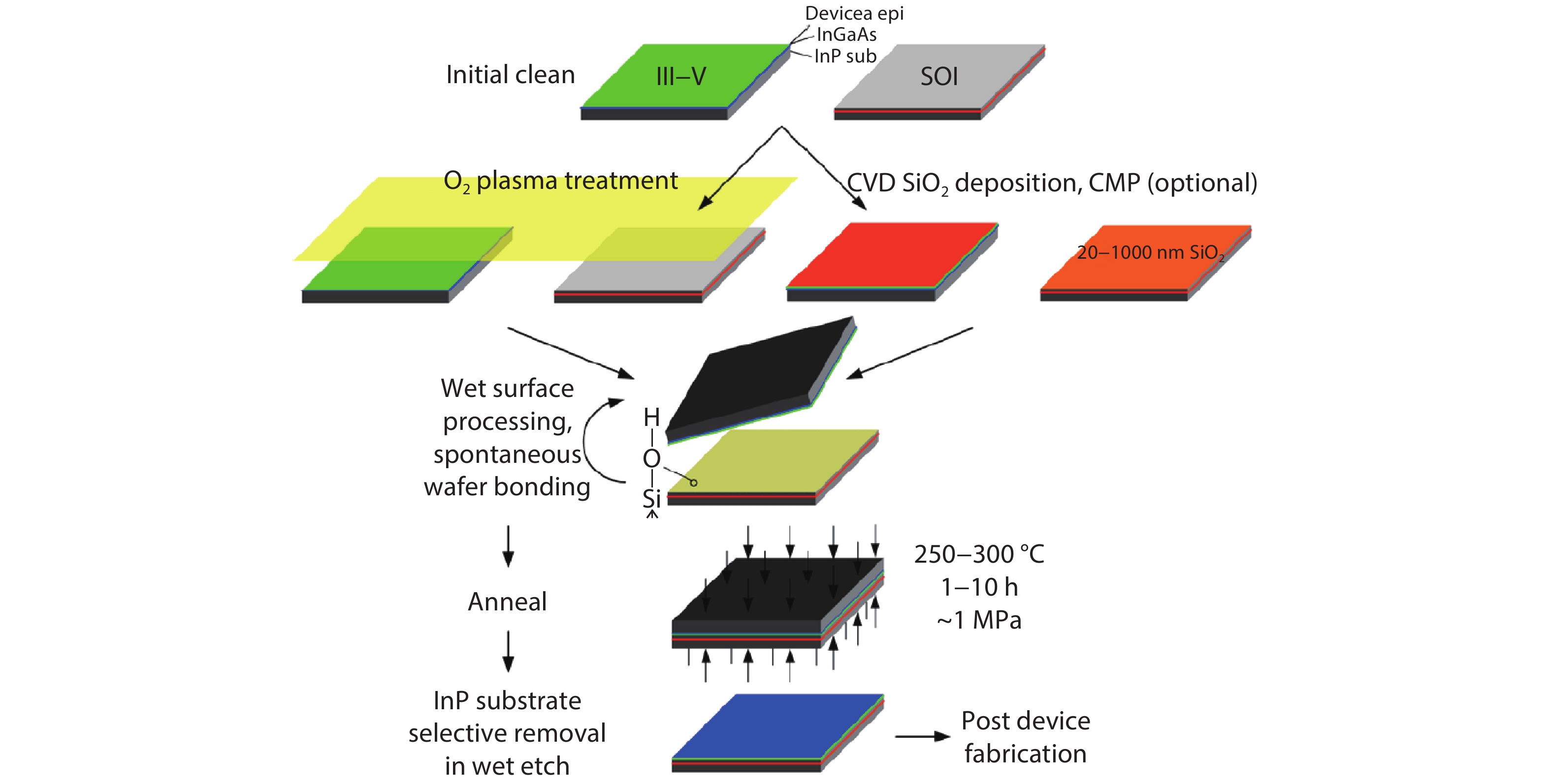
![(Color online) Schematic O2 plasma-assisted and SiO2 covalent wafer bonding process flow. Reproduced from Ref. [15].](/richHtml/jos/2019/40/10/101304/img_1.jpg)
Fig. 1. (Color online) Schematic O2 plasma-assisted and SiO2 covalent wafer bonding process flow. Reproduced from Ref. [15 ].
![(Color online) Schematic process flow for DVS-BCB adhesive bonding, referred to as “cold bonding”. Reproduced from Ref. [17].](/richHtml/jos/2019/40/10/101304/img_2.jpg)
Fig. 2. (Color online) Schematic process flow for DVS-BCB adhesive bonding, referred to as “cold bonding”. Reproduced from Ref. [17 ].
Fig. 3. (Color online) (a) Side view of the proposed hybrid laser structure and the evolution of the lasing supermode power transfer between the upper amplifying III–V section and adiabatic tapered lower silicon waveguide. (b) Refractive index profile of the coupled system. (c) Even supermode of the coupled system (at the phase-matching point). (d) Odd supermode of the coupled system (at the phase-matching point). Reproduced from Refs. [23 , 24 ].
Fig. 4. (Color online) (a) Three-dimensional view of the coupling structure in the gain section with representative mode profiles in two cross-sections. (b) Coupling power transmission and reflection. Reproduced from Ref. [21 ].
Fig. 5. (Color online) Schematics of heterogeneous integration of Si waveguides and III–V laser sources through (a)–(d) taper coupler, (f)–(i) slot coupler and (k)–(n) bridge-SWG coupler. (e), (j) and (o) Mode transformation from Si taper waveguide, Si slot waveguide, Si bridge-SWG waveguide to III–V lasers, the coupling ranges are from 0 to 4 μ m, 0 to 5.5 μ m, 0 to 5 μ m, respectively. Reproduced from Ref. [29 ].
Fig. 6. (Color online) (a, b) Schematic of the III–V-on-silicon DFB laser array and SEM image of the longitudinal cross section of the gain section. (c) Normalized lasing spectra of four 700 μ m long DFB lasers with a grating pitch ranging from 343 to 357 nm. (d, e) Evolution of the lasing spectra as a function of the bias current (20 mA step) for four DFB lasers with different gain section widths and silicon grating pitches of 353 nm (left) and 357 nm (right). Reproduced from Ref. [38 ].
Fig. 7. (Color online) (a–c) Illustration and microscope image of the anti-colliding III–V-on-Si MLL design. (d) Optical comb generated by the passively locked 1 GHz MLL with details of evenly spaced optical modes in the comb. (e) Beat between the optical comb and the tunable laser at a wavelength of 1600 nm. (f) Measured optical linewidth of the MLL indicates an optical linewidth below 250 kHz (delayed self-heterodyne method). The black dots are the measured data, and the red curve is the corresponding Lorentzian fitting. Reproduced from Ref. [44 ].
Fig. 8. (Color online) InP PhC nanolaser bonded on Si . (a) SEM image of the fabricated hybrid nanolaser after metallic contact deposition. (b) Optical microscope image of the structure in its final stage. (c) Emission wavelength and spectral linewidth against injection current at room temperature; inset: lasing spectrum at an injection current of 150 μ A. (d) L–I–V measurements of the nanolaser at room temperature. Reproduced from Ref. [57 ].
|
Table 1. Overall comparison between different III–V lasers integration strategies on silicon.
|
Table 2. General characteristics of direct bonding and adhesive bonding.

Set citation alerts for the article
Please enter your email address


