
Xuhan Guo, An He, Yikai Su. Recent advances of heterogeneously integrated III–V laser on Si[J]. Journal of Semiconductors, 2019, 40(10): 101304
- Journal of Semiconductors
- Vol. 40, Issue 10, 101304 (2019)
Abstract
1. Introduction
By exploiting mature and standard microelectronics CMOS processes, silicon photonics[
Recently, substantial efforts have been devoted toward light sources on Si by monolithic integration or hybrid integration. Monolithically integrated on-chip light sources are regarded to be the ultimate goal of silicon lasers, as the epitaxial growth may realize the high-density integration of lasers in Si photonics economically if the CMOS compatibility could be well solved. Because of the dissimilarity between III–V and group IV materials however, there are several fundamental challenges such as the threading dislocations (TDs), antiphase boundaries (APBs) and different coefficient of thermal expansion. The TDs are due to the large lattice constant mismatch (i.e. 8% for InP/Si and 4% for GaAs/Si) which could result in strain on the epilayer that render poor quality of III–V materials and also compromise the device performance; The APBs caused by the polar (III–Vs) and nonpolar (Si substrates) property could form the electrically charged planar defects acting as non-radiative recombination centers and current leakage paths for optoelectronic devices; The thermal coefficient gap however will create the thermal cracks between epilayers that preventing thicker III–Vs layers grown on Si. Recently, III–V quantum dot (QD) material has revolutionized monolithic integration of III–V light sources on Si over quantum well (QW) counterparts as being less sensitive to defects and temperature[
Heterogeneous integration, referring to III–V gain material on die/wafer-level or even complete devices transferred to Si substrates via a variety of chemical or physical bonding techniques, such that light generated in the III–V epitaxial layers is evanescently coupled into silicon circuits vertically. Compared with monolithic integration, this approach has much higher tolerance in lattice mismatch, and combines the excellent III–V light sources and superior Si passive waveguide components together. On the other hand, the clear advantage over hybrid integration lies in that no stringent positioning alignment is necessary. In general, heterogeneous integration approach could utilize the highly precise lithography to process III–V thin films and align the III–V gain devices with underneath bonded wafer-level SOI circuit, enabling potentially lower cost and high density of integration, is now considered as the most feasible way toward efficient Si laser integration. Heterogeneous integration itself can be differentiated by direct bonding or indirect bonding in terms of whether an insertion layer is applied. Indirect bonding is mainly including metals or polymers such as divinylsiloxane-benzocyclobutane (DVS-BCB) to perform the adhesives in between. A good review of heterogeneous integration Si laser is recently published in Ref. [13].
The overall comparison among the different III–V lasers integration methods on silicon are summarized in Table 1.
In this review paper, recent demonstrated heterogeneous integration of III–V lasers on Si will be presented with a special focus on direct/adhesive bonding enabling procedures. We will start by introducing the main bonding technologies, followed by the optical coupling structures for III–V/Si light routing. Then we will review the latest advance of heterogeneously integrated III–V lasers on Si, including DFB laser array, comb laser and one-dimensional (1D) photonic crystal cavity (PhC) laser. In the final section, we will have a discussion and summary.
2. Bonding technology
By combining known-good III–V epitaxial layer with silicon photonics via bonding technology, one can take advantage of the mature CMOS compatible processing, while maintaining utilizing III–V materials as on-chip light sources and allowing wafer-scale processing of devices after bonding.
2.1. Direct bonding
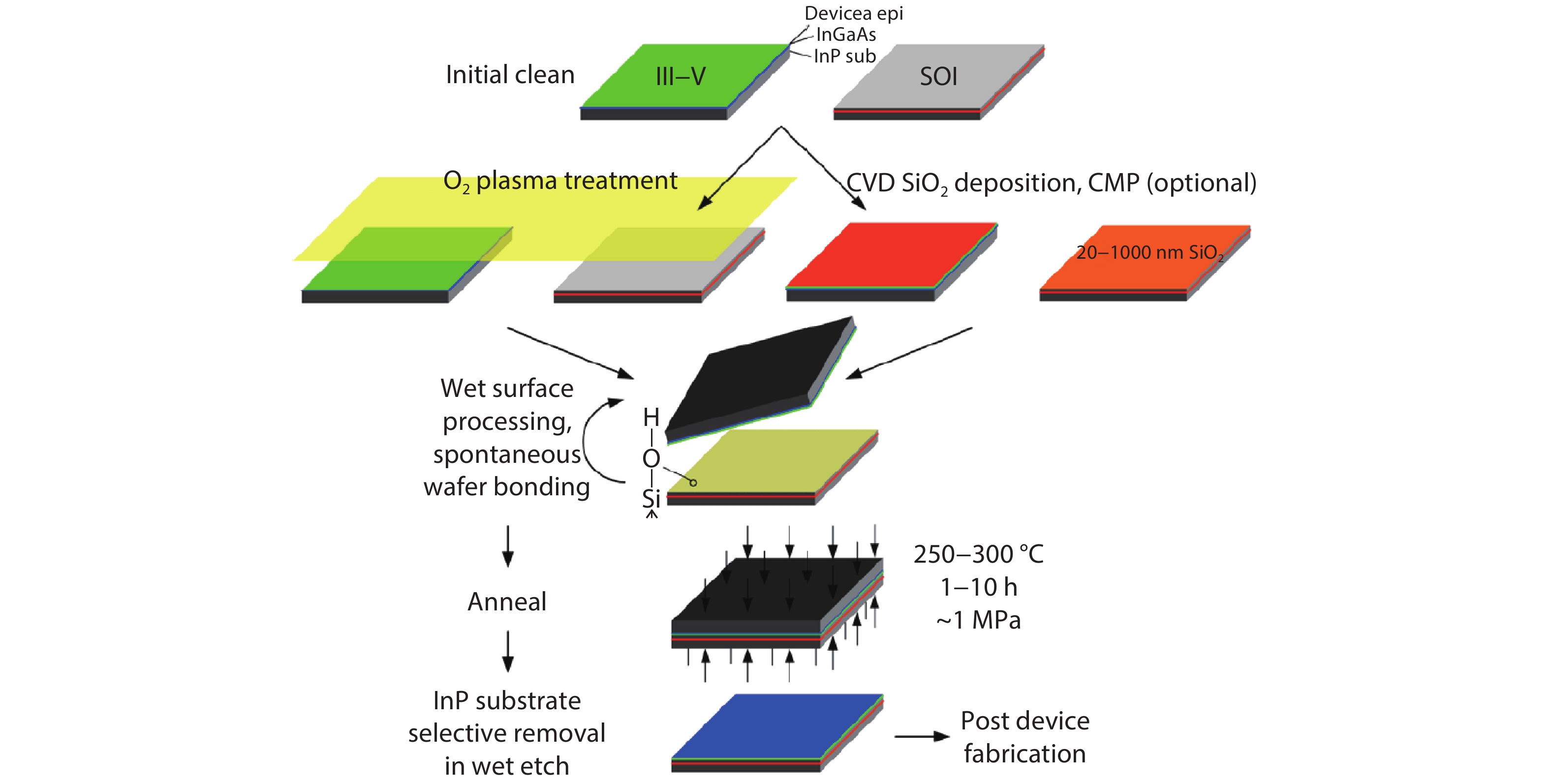
Direct bonding is a technique that brings stringently polished, flat and clean wafers or dies preparation into contact for integration. The general fabrication process to improve the bonding strength is rather complex, including the ultraclean conditions and atom-scale smooth surfaces. Besides, the high-temperature SOI processing (> 600 °C) will greatly damage the III–V wafer during manufacturing process, so special procedure is required to strictly prohibit a high-temperature anneal[
![]()
Figure 1.(Color online) Schematic O2 plasma-assisted and SiO2 covalent wafer bonding process flow. Reproduced from Ref. [
1. Hydrophobic surfaces clean: Prepare samples to remove the native oxide in standard buffered HF solution (SOI) or 39% NH4OH (InP).
2. O2 plasma treatment: Prepare samples in an O2 plasma surface treatment to grow an ultra-thin (~15 nm) plasma oxide layer with smooth (RMS roughness < 0.5 nm) hydrophilic surfaces. Especially, the O 2 energetic ion bombardment can efficiently remove hydrocarbons and water attached dirties on the sample surface.
3. SiO2 covalent bonding: Deposit SiO2 using PECVD on both surfaces or thermally grow SiO2 on Si to clean the hydrophilic surface. Employ chemical mechanical polishing (CMP) to improve surface topography and make sure the surface RMS roughness less than 1 nm.
4. Activation process: Passivate the two surfaces with a high density of polar hydroxyl groups (–OH), bridge bonds between the mating surfaces, enable spontaneous bonding at room temperature. O2 plasma-treated samples are dipped in deionized water and blow-dried or placed in a vaporized NH4OH environment. Thick SiO2-covered samples are boiled in diluted RCA-1 solution at 75 °C for 10 min, a step to clean and form an Si–OH-passivated surface, then blow dried. Similar O2 plasma treatment[
5. Anneal and cooling: Anneal the bonded sample at 300 °C with external coaxial pressure (1–2 MPa) for more than one hour after immediate physical mating typically in air at room temperature.
6. Selective InP substrate removal: Selectively remove the InP substrate in a 3HCl : 1H2O solution to leave thin (< 2μm) InP-based epitaxial layers on Si at room temperature after annealing and cooling process.
2.2. Adhesive bonding
The fabrication procedures of adhesive bonding by DVS-BCB are much more relaxed and not limited by the material dissimilarities. DVS-BCB is an excellent adhesive exhibiting good physical properties such as high bond strength, high degree of planarization, high optical clarity, good thermal stability, low refractive index and curing temperature[
![]()
Figure 2.(Color online) Schematic process flow for DVS-BCB adhesive bonding, referred to as “cold bonding”. Reproduced from Ref. [
1. Surface clean and BCB dilution: Immerse the sample into a standard clean (SC-1) solution (i.e., NH4OH : H2O2 : H2O 1 : 1 : 5) and heat for 15 min at 70 °C or by using a microwave O2 plasma to clean the SOI. Dilute the DVS-BCB with mesitylene then spin-coated onto the SOI substrate, thin bonding layer thickness (< 50 nm) can be achieved for better coupling to the topography of the silicon PIC.
2. Pre-curing: Pre-cure the spun DVS-BCB to evaporate all the solvents and partially polymerized, thereby improving the bonding layer thickness uniformity. Afterwards, deposite a thin (< 10 nm) silicon oxide layer to improve the adhesion to DVS-BCB.
3. Substrate removal and mounting: Remove the InP/InGaAs sacrificial layer pair on the III–V wafer/die is by selective wet etching using HCl : H2O (4 : 1) and H2SO4 : H2O2 : H2O solutions (1 : 1 : 18), so as to removes particles and contaminants from the III–V die surface prior to bonding. Then rinse the III–V die with DI water, dry and mount on the SOI die at room temperature by using low accuracy 500 μm alignment machine or more accurately using a flip-chip machine.
4. Bonding: Bring the III–V dies into contact with the DVS-BCB coated silicon photonics substrate and load in a wafer bonder. After pumping to vacuum and heating the sample to 150 °C with a ramp of 15 °C/min for 10 min, bonding pressure between 200 to 400 kPa is applied. Then further increase the temperature to 280 °C with a ramp of 1.5 °C/min and fully cure for one hour. After the curing, cool down the bonded samples (at 6–10 °C/min) and unload from the processing chamber.
5. Post processing: Remove the III–V substrate by grinding or by a selective wet etching using HCl. Transfer the III–V membrane to a Si sample with the functional layers bonded to the SOI die to get ready for further processing.
The adhesive bonding is very versatile due to the much simpler bonding process, virtually can apply to any compound semiconductor. Multiple die bonding and full wafer bonding have been already demonstrated[
3. Coupling structures
For heterogeneous integration of Si laser, there are several important requirements like the low coupling loss, small footprint and an overall high assembly yield, along with the low cost and large-scale production capability. Among various Si/III–V heterogeneously integrated devices by employing direct and adhesive bonding technologies, a common criterion is how to design a compact yet efficient light coupling structure to transfer the optical mode from an active III–V light sources to a silicon photonic circuits. There have been several coupling methods, including vertical[
From the theory of coupled waveguides, the adiabatic coupler doesn’t rely on evanescent tails, but by using taper that transforms the modes into supermodes of two or more coupled waveguide system instead[
![]()
Figure 3.(Color online) (a) Side view of the proposed hybrid laser structure and the evolution of the lasing supermode power transfer between the upper amplifying III–V section and adiabatic tapered lower silicon waveguide. (b) Refractive index profile of the coupled system. (c) Even supermode of the coupled system (at the phase-matching point). (d) Odd supermode of the coupled system (at the phase-matching point). Reproduced from Refs. [
Typical inverted adiabatic taper coupling structure design in a heterogeneously integrated distributed feedback (DFB) Si laser has been exploited[
![]()
Figure 4.(Color online) (a) Three-dimensional view of the coupling structure in the gain section with representative mode profiles in two cross-sections. (b) Coupling power transmission and reflection. Reproduced from Ref. [
Although the adiabatic tapered couplers have been proved to be robust, high efficient and broadband[
![]()
Figure 5.(Color online) Schematics of heterogeneous integration of Si waveguides and III–V laser sources through (a)–(d) taper coupler, (f)–(i) slot coupler and (k)–(n) bridge-SWG coupler. (e), (j) and (o) Mode transformation from Si taper waveguide, Si slot waveguide, Si bridge-SWG waveguide to III–V lasers, the coupling ranges are from 0 to 4
Through theoretically analysis, the optical mode coupling process between Si taper and III–V first section without p-InP layer determines the final coupling efficiency. The SOI chip and III–V materials are bonded through a 50 nm thick BCB layer. The Si coupler width shrinks from 600 to 150 nm at the length of 3 μm. Upon the Si taper, the width of n-InP taper increases from 1 to 2 μm, and the widths of tapered SCH and MQW layers are all from 150 to 500 nm.
In their design, the multistep or complex shape tapered structure is chosen to reduce the CL as shown in Fig. 5. The optimized III–V tapered coupler consists of three sections. The first section (L1) is a vertical coupler, and partially covered with a 1 μm tapered p-InP layer (L2) which is the second section. The third section is a 1 μm long tapered III–V materials (L3). These three coupling structures possess excellent compactness which is highly demanded for Si PIC, the entire CL is only 4 μm for taper coupler (Figs. 5(a)–5(d)), 5.5 and 5 μm for slot coupler (Figs. 5(f)–5(i)) and bridge-SWG coupler (Figs. 5(k)–5(n)) respectively. These couplers are the most compact compared with other state-of-the-art couplers. In addition, high efficiency and high fabrication tolerance can be achieved at the same time. For such short couplers, the fundamental TE mode coupling efficiency can still reach 93.7% and 95.5% for slot and bridge-SWG couplers at the wavelength of 1550 nm, respectively. Especially for the bridge-SWG coupler, the fundamental TE mode coupling efficiency can maintain higher than 90% in 100 nm wavelength range when the Si taper tip width varies from 100 to 200 nm. These ultra-compact couplers, which can be practically fabricated by existing technology, also exhibit outstanding fabrication tolerances.
4. New advances in bonding based heterogeneous integration technologies
For heterogeneous integrated Si lasers, the ability to change structures of both III–V components plus the additional degree of optimizing the bonded silicon/III–V cross-section have greatly enhanced the overall performance. Compared with monolithic III–V lasers on PICs which has significant incident photon density flux on exposed III–V facets, heterogeneously integrated active components have no related degradation mechanisms hence can greatly improve their reliability by minimizing III–V facet. Various structures of heterogeneously integrated III–V components on silicon platform have been demonstrated with continuously improved performance comparable or even better than their native III–V counterparts with more complex PICs over the past decade, some previous intensive reviews can be found in Refs. [28, 31, 32], here we give an overview of recent advances of the heterogeneous integrated Si lasers, including III–V DFB array, III–V comb laser and III–V PhC nanolasers on Si for emerging applications like spectroscopy, sensing, metrology and microwave photonics.
4.1. III–V DFB laser array on Si
Due to efficient phase shift, single wavelength mode and low spectral Lorentzian linewidth, various DFB lasers on heterogeneous silicon photonics platform have been studied since the first demonstration[
Apart from traditional applications in data communications utilizing from the near-infrared to some of mid-infrared (MIR) wavelengths (1.1–8 μm), MIR (2–20 μm) region has shown great potential for many applications including spectroscopy, thermal imaging and free-space communication[
![]()
Figure 6.(Color online) (a, b) Schematic of the III–V-on-silicon DFB laser array and SEM image of the longitudinal cross section of the gain section. (c) Normalized lasing spectra of four 700
4.2. III–V comb lasers on Si
Optical-frequency combs have revolutionized the research field of frequency metrology by connecting the radio frequency (RF) domain and the optical domain, which can precisely measure the optical frequencies by the down-conversion to the RF domain. Optical-frequency combs vision a wide range of exciting applications, including the construction of optical clocks[
Recently a new III–V/Si ultra-dense comb laser[
![]()
Figure 7.(Color online) (a–c) Illustration and microscope image of the anti-colliding III–V-on-Si MLL design. (d) Optical comb generated by the passively locked 1 GHz MLL with details of evenly spaced optical modes in the comb. (e) Beat between the optical comb and the tunable laser at a wavelength of 1600 nm. (f) Measured optical linewidth of the MLL indicates an optical linewidth below 250 kHz (delayed self-heterodyne method). The black dots are the measured data, and the red curve is the corresponding Lorentzian fitting. Reproduced from Ref. [
4.3. III–V PhC nano lasers on Si
Compact and energy efficient active components are very important in application like the optical interconnects on a silicon PIC. Wavelength-scale PhC resonators provide enhanced light-mater interactions and control of spontaneous emission, has exhibited the highest quality value (Q) reported over modal volume ratios, which make possible the low-threshold, thresholdless laser emission or efficient all-optical switching[
Université Paris-Sud has recently reported the InP PhC lasers heterogeneously integrated on Si by BCB bonding[
![]()
Figure 8.(Color online) InP PhC nanolaser bonded on Si . (a) SEM image of the fabricated hybrid nanolaser after metallic contact deposition. (b) Optical microscope image of the structure in its final stage. (c) Emission wavelength and spectral linewidth against injection current at room temperature; inset: lasing spectrum at an injection current of 150
5. Discussion and conclusion
We have reviewed the recently demonstrated heterogeneous integration of III–V lasers on Si with a special focus on direct/adhesive bonding enabling methods, coupling structures for III–V/Si light routing and novel laser configurations for applications beyond traditional telecommunications. Tremendous progress in heterogeneous integration with years of extensive R&D presents opportunities for the realization of on-chip Si light sources or novel device architectures with additional functions and enhanced performance, exhibits the highest maturity combining the strengths of both III–V platform and silicon photonics platform. This approach allows wafer-scale processing of devices after bonding III–V thin films on silicon, enables potentially lower cost, greatly relaxed alignment tolerance and high density of integration. Especially the adhesive bonding could be versatile to implement on-chip light sources for a varsity of applications with the scalability for high-volume and low-cost fabrication demand. Traditional data communications with high dense intra- and inter-chip interconnections, next-generation processors and high-performance computing have been the primary drive for the development forward as the aforementioned newly demonstrated directly modulated 50 Gb/s[
For the evolution of photonic integrated circuits, the prevailing trend that drives the evolution of PICs is higher integration density, lower cost and higher power efficiency following the performance and economic development. From research side, a number of foundries such as AIM Photonics, CEA-LETI, IMEC and IME are currently exploring this process of integrating III–V materials with CMOS scaling. The heterogeneous integration Si laser is also preferred by industry for the commercial deployment, an encouraging step of such is that Intel has released the successful silicon photonics quad small form-factor pluggable (QSFP) format transceiver in CMOS Foundry that supports 100G communications in 2016[
However, there are still some difficulties to overcome in heterogeneous integration that cause some degradation compared with the III–V devices on their native substrate. For direct bonding method, due to the stringent requirements of ultraclean and extremely smooth surfaces, the associated complexity is still considerable. For adhesive bonding method, the heat dissipation is challenging due to the high thermal resistance introduced by the bonding layer and the underlying buried oxide, rendering some difficulties of integrate high-density laser devices on Si chips. Although for monolithic integration method, the practical light sources, such as the electrical pumping, active-passive coupling, wafer-scale epitaxy technique and high yield and reliability still need huge efforts, it’s fair to say that in the long term, monolithic integration of QD lasers on SOI platform represents the most promising integration approach for realizing reliable, power efficient, high-density integration of laser diodes on silicon chips. This may enable a major breakthrough towards the realization of large-scale, cost-effective full functional silicon photonics. Especially the V-groove growth technique that allows the co-integration of III–V and Si photonic components as well as electronic devices while avoiding thick buffer layers and non-standard wafers.
In summary, up to date, with the combination of high-quality III–V material, novel Si photonic design and advanced fabrication techniques with more efforts in R&D plus the continuing impetus from new areas of applications, heterogeneously integrated Si laser sources may extend to more interesting research areas and commercial mass-production in the near future.
Acknowledgments
This work was supported by Natural Science Foundation of China (NSFC) under Grant 61805137, Natural Science Foundation of Shanghai under Grant 19ZR1475400, Shanghai Sailing Program under Grant 18YF1411900 and the Open Project Program of Wuhan National Laboratory for Optoelectronics No. 2018WNLOKF012
References
[1] C Doerr. Silicon photonic integration in telecommunications. Front Phys Rev, 3(2015).
[2] R Soref. The past, present, and future of silicon photonics. IEEE J Sel Top Quantum Electron, 12, 1678(2006).
[3] M J R Heck, J F Bauters, M L Davenport et al. Ultra-low loss waveguide platform and its integration with silicon photonics. Laser Photonics Rev, 8, 667(2014).
[4] T R Graham, Z M Goran, Frederic Y G Y. et al. Recent breakthroughs in carrier depletion based silicon optical modulators. Nanophotonics, 3, 229(2014).
[5] G T Reed, G Mashanovich, F Y Gardes et al. Silicon optical modulators. Nat Photon, 4, 518(2010).
[6] M Casalino, G Coppola, R M De La Rue et al. State-of-the-art all-silicon sub-bandgap photodetectors at telecom and datacom wavelengths. Laser Photonics Rev, 10, 895(2016).
[7] T David, Z Aaron, E B John et al. Roadmap on silicon photonics. J Opt, 18, 073003(2016).
[8] H Liu, T Wang, Q Jiang et al. Long-wavelength InAs/GaAs quantum-dot laser diode monolithically grown on Ge substrate. Nat Photon, 5, 416(2011).
[9] S Zhu, B Shi, Q Li et al. Room-temperature electrically-pumped 1.5
[10] A Y Liu, C Zhang, J Norman et al. High performance continuous wave 1.3
[11] M Liao, S Chen, J S Park et al. III–V quantum-dot lasers monolithically grown on silicon. Semicond Sci Technol, 33, 123002(2018).
[12] N Hatori, T Shimizu, M Okano et al. A hybrid integrated light source on a silicon platform using a trident spot-size converter. J Lightwave Technol, 32, 1329(2014).
[13] M L Davenport, M A Tran, T Komljenovic et al. Heterogeneous integration of III–V lasers on Si by bonding. Semiconductors and Semimetals, 99, 139(2018).
[14] T Komljenovic, M Davenport, J Hulme et al. Heterogeneous silicon photonic integrated circuits. J Lightwave Technol, 34, 20(2016).
[15] D Liang, G Roelkens, R Baets et al. Hybrid integrated platforms for silicon photonics. Materials, 3, 1782(2010).
[16] D Liang, M Fiorentino, S Srinivasan et al. Low threshold electrically-pumped hybrid silicon microring lasers. IEEE J Sel Top Quantum Electron, 17, 1528(2011).
[17] S Keyvaninia, M Muneeb, S Stanković et al. Ultra-thin DVS-BCB adhesive bonding of III–V wafers, dies and multiple dies to a patterned silicon-on-insulator substrate. Opt Mater Express, 3, 35(2013).
[18] J Van Campenhout, P Rojo-Romeo, P Regreny et al. Electrically pumped InP-based microdisk lasers integrated with a nanophotonic silicon-on-insulator waveguide circuit. Opt Express, 15, 6744(2007).
[19] Y D Koninck, G Roelkens, R Baets. Design of a hybrid III–V-on-silicon microlaser with resonant cavity mirrors. IEEE Photonics J, 5, 2700413(2013).
[20] B Ben Bakir, A Descos, N Olivier et al. Electrically driven hybrid Si/III–V Fabry-Pérot lasers based on adiabatic mode transformers. Opt Express, 19, 10317(2011).
[21] S Keyvaninia, G Roelkens, D Van Thourhout et al. Demonstration of a heterogeneously integrated III–V/SOI single wavelength tunable laser. Opt Express, 21, 3784(2013).
[22] S Keyvaninia, S Verstuyft, L Van Landschoot et al. Heterogeneously integrated III–V/silicon distributed feedback lasers. Opt Lett, 38, 5434(2013).
[23] X Sun, H C Liu, A Yariv. Adiabaticity criterion and the shortest adiabatic mode transformer in a coupled-waveguide system. Opt Lett, 34, 280(2009).
[24] X Sun, A Yariv. Engineering supermode silicon/III–V hybrid waveguides for laser oscillation. J Opt Soc Am B, 25, 923(2008).
[25] A Yariv, X Sun. Supermode Si/III–V hybrid lasers, optical amplifiers and modulators: A proposal and analysis. Opt Express, 15, 9147(2007).
[26] G Kurczveil, M J R Heck, J D Peters et al. An integrated hybrid silicon multiwavelength AWG laser. IEEE J Sel Top Quantum Electron, 17, 1521(2011).
[27] S Uvin, S Kumari, A De Groote et al. 1.3
[28] J E Bowers, D Huang, D Jung et al. Realities and challenges of III–V/Si integration technologies. Optical Fiber Communication Conference (OFC), Tu3E.1(2019).
[29]
[30] D Ohana, U Levy. Mode conversion based on dielectric metamaterial in silicon. Opt Express, 22, 27617(2014).
[31] Z Wang, A Abbasi, E Dave et al. Novel light source integration approaches for silicon photonics. Laser Photonics Rev, 11, 1700063(2017).
[32] G Roelkens, L Liu, D Liang et al. III–V/silicon photonics for on-chip and intra-chip optical interconnects. Laser Photonics Rev, 4, 751(2010).
[33] A W Fang, E Lively, Y H Kuo et al. A distributed feedback silicon evanescent laser. Opt Express, 16, 4413(2008).
[34] A Abbasi, S Keyvaninia, t J Verbist et al. 43 Gb/s NRZ-OOK direct modulation of a heterogeneously integrated InP/Si DFB laser. J Lightwave Technol, 35, 1235(2017).
[35] A Abbasi, B Moeneclaey, J Verbist et al. Direct and electroabsorption modulation of a III–V-on-silicon DFB laser at 56 Gb/s. IEEE J Sel Top Quantum Electron, 23, 1(2017).
[36] Y Zou, S Chakravarty, C J Chung et al. Mid-infrared silicon photonic waveguides and devices. Photonics Res, 6(2018).
[37] R Wang, S Sprengel, A Malik et al. Heterogeneously integrated IIIV-on-silicon 2.3x
[38] R Wang, S Sprengel, G Boehm et al. Broad wavelength coverage 2.3
[39] P J Delfyett, D H Hartman, S Z Ahmad. Optical clock distribution using a mode-locked semiconductor laser diode system. J Lightwave Technol, 9, 1646(1991).
[40] N Picqué, T W Hänsch. Frequency comb spectroscopy. Nat Photonics, 13, 146(2019).
[41] J Mandon, G Guelachvili, N Picqué. Fourier transform spectroscopy with a laser frequency comb. Nat Photonics, 3, 99(2009).
[42] A L Gaeta, M Lipson, T J Kippenberg. Photonic-chip-based frequency combs. Nat Photonics, 13, 158(2019).
[43] D T Spencer, T Drake, T C Briles et al. An optical-frequency synthesizer using integrated photonics. Nature, 557, 81(2018).
[44] Z Wang, K Van Gasse, V Moskalenko et al. A III–V-on-Si ultra-dense comb laser. Light: Sci Appl, 6, e16260(2017).
[45] G Dong, W Deng, J Hou et al. Ultra-compact multi-channel all-optical switches with improved switching dynamic characteristics. Opt Express, 26, 25630(2018).
[46] H Altug, D Englund, J Vučković. Ultrafast photonic crystal nanocavity laser. Nat Phys, 2, 484(2006).
[47] K Nozaki, T Tanabe, A Shinya et al. Sub-femtojoule all-optical switching using a photonic-crystal nanocavity. Nat Photonics, 4, 477(2010).
[48] S Matsuo, A Shinya, T Kakitsuka et al. High-speed ultracompact buried heterostructure photonic-crystal laser with 13 fJ of energy consumed per bit transmitted. Nat Photonics, 4, 648(2010).
[49] C Monat, C Seassal, X Letartre et al. InP 2D photonic crystal microlasers on silicon wafer: room temperature operation at 1.55
[50] G Vecchi, F Raineri, I Sagnes et al. Photonic-crystal surface-emitting laser near 1.55
[51] K Tanabe, M Nomura, D Guimard et al. Room temperature continuous wave operation of InAs/GaAs quantum dot photonic crystal nanocavity laser on silicon substrate. Opt Express, 17, 7036(2009).
[52] T J Karle, Y Halioua, F Raineri et al. Heterogeneous integration and precise alignment of InP-based photonic crystal lasers to complementary metal-oxide semiconductor fabricated silicon-on-insulator wire waveguides. J Appl Phys, 107, 063103(2010).
[53] K Takeda, T Sato, A Shinya et al. Few-fJ/bit data transmissions using directly modulated lambda-scale embedded active region photonic-crystal lasers. Nat Photonics, 7, 569(2013).
[54] G Crosnier, D Sanchez, A Bazin et al. High
[55] K A Atlasov, M Felici, K F Karlsson et al. 1D photonic band formation and photon localization in finite-size photonic-crystal waveguides. Opt Express, 18, 117(2010).
[56] M K Seo, K Y Jeong, J K Yang et al. Low threshold current single-cell hexapole mode photonic crystal laser. Appl Phys Lett, 90, 171122(2007).
[57] G Crosnier, D Sanchez, S Bouchoule et al. Hybrid indium phosphide-on-silicon nanolaser diode. Nat Photon, 11, 297(2017).
[58] T Spuesens, F Mandorlo, P Rojo-Romeo et al. Compact integration of optical sources and detectors on soi for optical interconnects fabricated in a 200 mm CMOS pilot line. J Lightwave Technol, 30, 1764(2012).
[59] K Y Jeong, Y S No, Y Hwang et al. Electrically driven nanobeam laser. Nat Commun, 4, 2822(2013).
[60] W Kobayashi, T Ito, T Yamanaka et al. 50-Gb/s direct modulation of a 1.3-
[61] H Kim, W J Lee, A C Farrell et al. Telecom-wavelength bottom-up nanobeam lasers on silicon-on-insulator. Nano Lett, 17, 5244(2017).
[62]

Set citation alerts for the article
Please enter your email address
© Copyright 2018-2021 | Chinese Laser Press. All Rights Reserved 沪ICP备15018463号-20