
Feilong Ding, Baokang Peng, Xi Li, Lining Zhang, Runsheng Wang, Zhitang Song, Ru Huang. A review of compact modeling for phase change memory[J]. Journal of Semiconductors, 2022, 43(2): 023101
- Journal of Semiconductors
- Vol. 43, Issue 2, 023101 (2022)
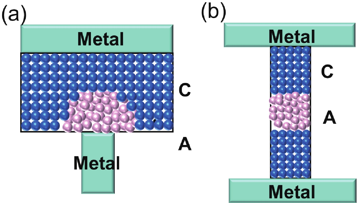
Fig. 1. (Color online) Schematics of two typical PCM cell structures: (a) the mushroom type and (b) the confinement type. In between the metal electrodes are the phase change materials, which show the crystalline phase (blue atoms in color) and amorphous phase (silver atoms in color).
![(Color online) (a) Stable phase states and the atomistic structures. (b) The phase change dynamics with RESET/SET/READ pulses. Reprinted by permission from Springer Nature Customer Service Centre GmbH: Springer Nature MRS Bulletin, Phase-change materials in electronics and photonics, Wei Zhang et al.[32], 2019.](/richHtml/jos/2022/43/2/023101/img_2.jpg)
Fig. 2. (Color online) (a) Stable phase states and the atomistic structures. (b) The phase change dynamics with RESET/SET/READ pulses. Reprinted by permission from Springer Nature Customer Service Centre GmbH: Springer Nature MRS Bulletin, Phase-change materials in electronics and photonics, Wei Zhang et al .[32 ], 2019.
Fig. 3. (Color online) Schematic diagram of the crystallization from the energy perspective. (a) The nucleation is described as a process with energy barrier of E a1 plus the energy of nucleus ΔG with the critical size r c. (b) The growth is described as a bi-directional process with a barrier of E a2 and a barrier of |dg |.
Fig. 4. Probability densities of nucleation and growth per nanosecond as given by the above CNG model. The bell-shaped characteristics have been widely used in PCM simulations in literature. Reprinted from Ref. [39 ], with the permission of AIP Publishing.
Fig. 5. (Color online) (a) Schematic diagram of three phases and their transitions and (b) dependence of the phase transition rates on temperature. © [2008] IEEE. Reprinted with permission from Ref. [40 ].
Fig. 6. (Color online) Schematic for the memory programing with desired temperature pulses. For a SET there can be two themes: a “solid phase crystallization” (SPC) and a “melting and slow cooling” (MSC). The slow cooling corresponds to a crystallization process below the melting temperature.
Fig. 7. (a) Core block of the model. (b) I–V curves from the macro model (line) in comparisons with the experimental data(dots). © [2006] IEEE. Reprinted with permission from Ref. [45 ].
Fig. 8. Flowchart of the binary macro model with different modules to decide the temperature and the phase. © [2006] IEEE. Reprinted with permission from Ref. [46 ].
Fig. 9. I–V characteristics of RESET and SET state, with temperature dependence following the Arrhenius law. The threshold switching is realized by a versatile function F which provides a smooth transition from the high-resistance to low-resistance state. © [2006] IEEE. Reprinted with permission from Ref. [50 ].
Fig. 10. (Color online) Crystallization dynamics as given by the JMAK theory and the experimental data under different temperatures. Temperature dependence of the time constant follows approximately the Arrhenius law. © [2007] IEEE. Reprinted with permission from Ref. [51 ].
Fig. 11. (Color online) Auxiliary circuits are introduced to implement the crystallization kinetics of Eq. (12). © [2007] IEEE. Reprinted with permission from Ref. [51 ].
Fig. 12. (Color online) A dynamic “versatile” function F for descriptions of the threshold switching process in the time domain.
Fig. 13. (Color online) (a) Current of the PCM versus voltage with vary amorphization fraction F a. Dots (experiments), lines (simulations). (b) R–I curve of PCM under different temperature. Dots (experiments), lines (simulations). © [2018] IEEE. Reprinted with permission from Ref. [53 ].
Fig. 14. (Color online) (a) Equivalent circuit model, including all the modules: the transport module, the thermal module and phase transition module. (b) Model compared with experiment data on I–V characteristic. © [2016] IEEE. Reprinted with permission from Ref. [54 ].
Fig. 15. (Color online) (a) The distribution of conductance values as a function of the number of partial SET pulses. Reprinted from Ref. [67 ], with the permission of AIP Publishing. (b) Modeling the gradual SET process where the crystalline ratio C f of the PCM is recorded after each pulse.
Fig. 16. (Color online) (a) Resistance as a function of time for the amorphous (reset) and crystalline (set) states of a PCM device. © [2010] IEEE. Reprinted with permission from Ref. [72 ]. (b) Resistance versus time for a reset cell. The two insets represent the mixed-phase structure for relatively short (top left) and long (bottom right) times during the bake experiment. © [2006] IEEE. Reprinted with permission from Ref. [73 ].

Set citation alerts for the article
Please enter your email address
© Copyright 2018-2021 | Chinese Laser Press. All Rights Reserved 沪ICP备15018463号-20