
Feilong Ding, Baokang Peng, Xi Li, Lining Zhang, Runsheng Wang, Zhitang Song, Ru Huang. A review of compact modeling for phase change memory[J]. Journal of Semiconductors, 2022, 43(2): 023101
- Journal of Semiconductors
- Vol. 43, Issue 2, 023101 (2022)
Abstract
1. Introduction to PCM and its modeling
Phase change memory[
As of today, PCM has entered the market of standalone memory, for example the 3D XPoint memory by Intel[
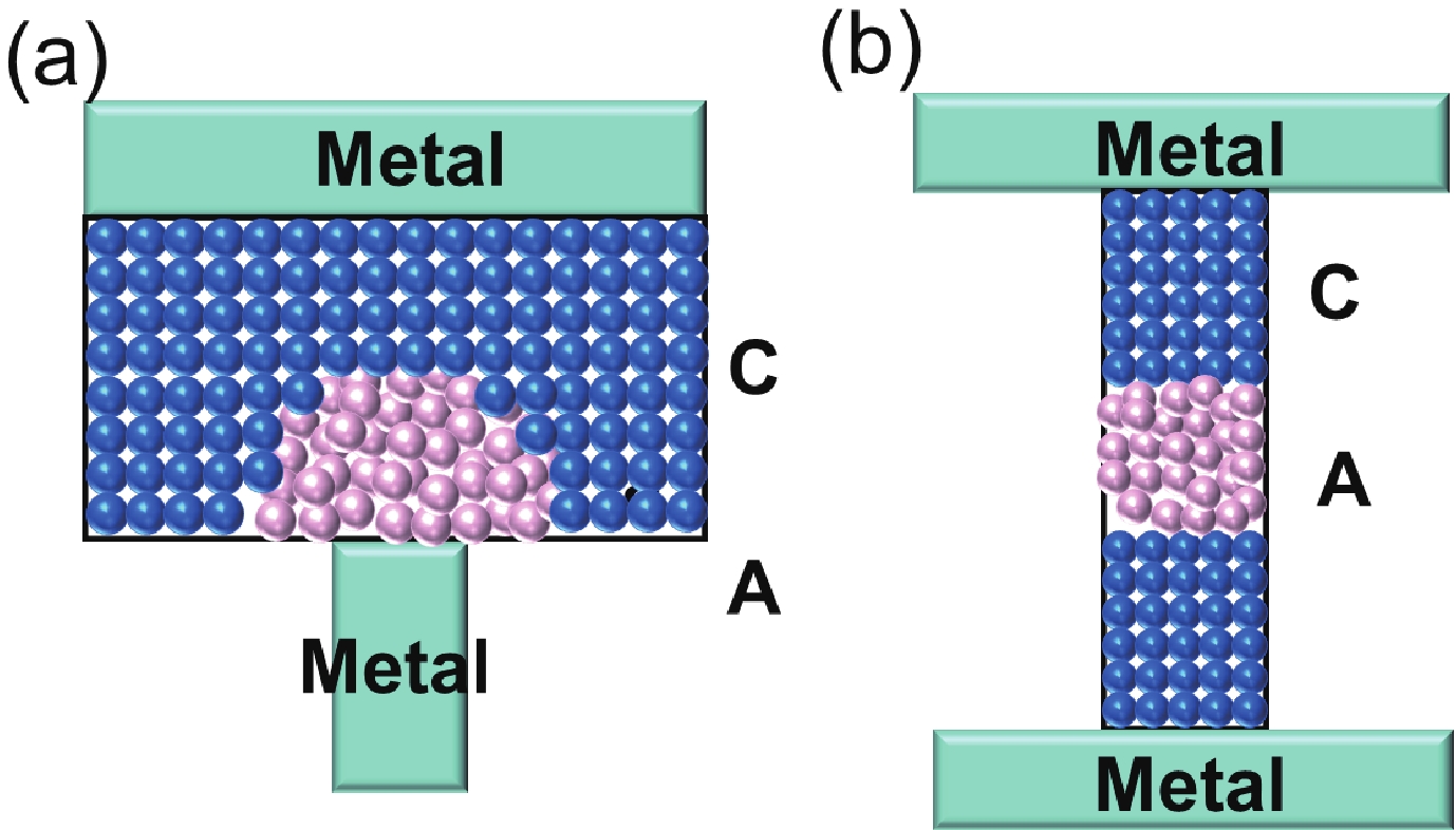
![]()
Figure 1.(Color online) Schematics of two typical PCM cell structures: (a) the mushroom type and (b) the confinement type. In between the metal electrodes are the phase change materials, which show the crystalline phase (blue atoms in color) and amorphous phase (silver atoms in color).
Along with advancements of the PCM technology, their compact models had been playing important roles. Memory device models are needed for the same purpose of all other device models: to be used for circuit simulations. Although the memory cells are generally repeated in an array or a chip and the reading operation is more or less regarded as a single cell operation, a memory model is still necessary for the memory technology development[
In this work we review compact models of the phase change memory. Device physics and principle operations as the basis of compact modeling are explained in Section 2. Then reported compact models of different categories from behavior macro models, to physics-based models with different approximations are reviewed in Section 3. Finally, further challenges on PCM modeling and our perspective are explained in Section 4.
2. Basic principle of PCM operations
There are three distinct states in the operations of PCM as shown in Fig. 2(a): the crystalline state (C), the amorphous state (A) and the melted liquid state (M), although only two of them (C and A) are possible at room temperature. The transition from state A to C is called crystallization. The transition from state C to A is not a direct process but via the state M, and is usually called amorphization. Fig. 2(b) shows the programing temperature for crystallization (also called SET) and amorphization (also called RESET). The SET process is triggered by increasing the temperature above the crystallization temperature (Tcryst or simplyTc). There are two possibilities in the process, a nucleation kinetics and a growth kinetics, that re-arrange atoms to form an ordered structure. The RESET process is triggered by increasing the temperature above the melting temperature (Tmelt or simplyTm) and then quenching, i.e., decreasing the temperature within a short period. In the process the crystalline structure is melted with the chemical bonds broken, and the atoms re-arrange forming a disordered structure. For memory applications, the energy in the SET and RESET process comes from the Joule heat of the electrical pulse. Some further details in addition to the above essential ones of PCM operations are reported in excellent reviews[
![]()
Figure 2.(Color online) (a) Stable phase states and the atomistic structures. (b) The phase change dynamics with RESET/SET/READ pulses. Reprinted by permission from Springer Nature Customer Service Centre GmbH: Springer Nature MRS Bulletin, Phase-change materials in electronics and photonics, Wei Zhang
Another key property for the SET process is the threshold switching. It refers to an increase in the conductance after the voltage across the amorphous region reaches a critical value. Only with the threshold switching property, Joule heating for increasing the temperature above Tc happens with a reasonable voltage, which otherwise will be too large for applications. In the current–voltage curves, a snap-back is defined as the region with decreasing voltage and increasing current, i.e., a negative differential resistance. The threshold switching effect provides a dynamic resistance which is comparable to the crystalline resistance to enable the SET process. While the physics of threshold switching is still yet to be fully investigated, there are a few proposals such as a thermal model[
A popular theory for the crystallization is the classical nucleation and growth (CNG) theory[
The nucleation probability Pn[
in which α is a frequency factor,β = 1/(kT) with k the Boltzmann constant and T the temperature. Detailed derivations have been reported in the literature[
![]()
Figure 3.(Color online) Schematic diagram of the crystallization from the energy perspective. (a) The nucleation is described as a process with energy barrier of
A deterministic model, which can be regarded as a variant of the above probabilistic model, has a similar formulation of the phase transition rate[
At the same time, the stabilized nucleus grows at any interface between the crystalline and amorphous. The growth is regarded as a combination of an atom diffusion Arrhenius process (with the activation energy Ea2) and a bi-directional process of liquid-solid transition. As a result, the growth velocity is given by[
in which
which is transformed from Eq. (4) with f replaced by an exponential factor, and p is a fitting parameter. Fig. 3(b) plots a schematic energy diagram for the growth process. Alternatively, the growth rate similar to the above nucleation rate is derived:
in which
The above Eqs. (2) and (5) have been used in a probabilistic framework[
![]()
Figure 4.Probability densities of nucleation and growth per nanosecond as given by the above CNG model. The bell-shaped characteristics have been widely used in PCM simulations in literature. Reprinted from Ref. [
Based on the CNG model, a phase space framework has been reported[
![]()
Figure 5.(Color online) (a) Schematic diagram of three phases and their transitions and (b) dependence of the phase transition rates on temperature. © [2008] IEEE. Reprinted with permission from Ref. [
Another theory to describe the crystallization is the Johnson–Mehl–Avrami–Kolmogorov (JMAK) theory[
in which w is a frequency factor and n is the Avrami coefficient, Ea is the activation energy. The JMAK theory may be regarded as an approximation of the CNG theory in a specific temperature range.
The PCM state, either SET, partial SET or RESET, can be achieved by designing the melting and cooling (usually termed as quenching) process. The RESET to high resistance can be done by a “melting and fast cooling” process after melting the memory active region, as shown in Fig. 2. Noticing the quenching time-dependent chalcogenide atoms re-organizations, the SET to low resistance can be done by a “melting and slow cooling” (MSC) method[
![]()
Figure 6.(Color online) Schematic for the memory programing with desired temperature pulses. For a SET there can be two themes: a “solid phase crystallization” (SPC) and a “melting and slow cooling” (MSC). The slow cooling corresponds to a crystallization process below the melting temperature.
3. Current status of PCM modeling
In this section, models with different approaches and different levels of abstractions are described, from the macro models, to more physics-oriented models.
3.1. Macro models
One key feature of the PCM is the switching from the amorphous state to crystalline state, or from the amorphous state to a dynamic on state. In the most common current–voltage characteristics, the above switching shows a snap-back. One essential starting point for a macro model is to find an appropriate representation for the device, either a pure mathematic one or a physics-based one for other well-studied devices. In the latter case, a lumped SPICE model may be generated by borrowing the formulations of devices with similar I–V and the switching.
3.1.1. Cobley’s model
A macro model of PCM was reported[
![]()
Figure 7.(a) Core block of the model. (b)
To model the snap-back, a silicon-controlled rectifier (SCR) type formulation was used for a softer transition from the high-resistance to low-resistance state. Some considerations on the transition smoothness are incorporated in the model with additional circuit components. Fig. 7(b) shows the I–V curves from the macro model in comparisons with the experimental data. For transient simulation, it is necessary to account for the duration of the input pulse, especially for the SET process. An extension to the Word circuit with an integrator is included to detect the input amplitude and duration, and only activates the switching when the crystallization/amorphization is expected to finish after a period.
3.1.2. Wei’s model
A similar macro model was reported[
![]()
Figure 8.Flowchart of the binary macro model with different modules to decide the temperature and the phase. © [2006] IEEE. Reprinted with permission from Ref. [
Macro models are relatively straightforward to be developed without knowing the device physics. As seen above, existing circuit blocks are connected to reproduce the observed PCM properties. The PCM macro models have been assisting the technology development at the early stage. One general drawback of macro models is a high complexity and long computational time. Thus physics-based models are usually pursued when the technology becomes more mature.
3.2. Physics-based model
3.2.1. Fantini’s model
A single piece model was reported[
![]()
Figure 9.
A smooth function F(x, xt) is proposed for the threshold switching behavior. It can be any function which switches from 0 to 1 around a threshold value x = xt. In practice, a Fermi-like function is a good option. For the PCM modeling, a parameter of threshold current (Ith) is used to represent the critical condition of threshold switching, and the current–voltage relationship is described by Eq. (10). Starting from the high resistance (e.g. fully amorphous) state, the current is given by Eq. (9) before it reaches Ith. Once the current reaches Ith, the smoothing F(I1, Ith) goes from zero to one, and the PCM switches to the crystalline state. The conduction is then described by the on state currentIon, which is part of the IαSET. The ‘versatile’ function provides a flexible description of the threshold switching, which is also termed as a voltage snap-back. Anyway, the current always increases, unlike the voltage drop across the PCM.
The cross point of the snap-back branch and theIαSET branch is (Vhold, Ihold), which satisfies the crystalline stateIαSET of Eq. (9) as well as the load line below:
in whichRload is the PCM load resistance (the resistance in series, e.g. the heater resistance).Vth is the threshold voltage. In the implementation, the PCM together with a given load resistance R is treated as a voltage controlled current source (VCCS). At the threshold voltage, the passing current changes from the IαRESET to Ion.
The model[
3.2.2. Ventrice’s model
An improved model without involving the table-based approach for crystallization was reported[
It is indeed identical to the JMAK theory with Avrami coefficient n = 1. The phase change material resistance is determined with Cx:
in which R0c and R0a the resistance of state which are completely crystallized and amorphized, respectively.
Fig. 10 shows that Eq. (12) agrees well with the experimental data of resistance evolution in the time domain under a certain temperature. With Eqs. (12) and (13), the crystallization process can be described step-by-step with the temperature at each step. For the implementation, auxiliary circuits in Fig. 11 to integrate for the crystal fraction Cx is introduced. A temperature circuit calculates the heat and obtains the temperature. Taking the temperature as inputs, the timer circuit accumulates time when the temperature is between the crystallization temperature Tc and melting temperature Tm. The crystal fraction circuit implements the Eq. (12) with inputs from the timer circuit. At the same time, Cx goes to zero once the temperature reaches Tm. The crystal fraction Cx is fed back into the current–voltage equations, and a self-consistency loop is implemented in the model.
![]()
Figure 10.(Color online) Crystallization dynamics as given by the JMAK theory and the experimental data under different temperatures. Temperature dependence of the time constant follows approximately the Arrhenius law. © [2007] IEEE. Reprinted with permission from Ref. [
![]()
Figure 11.(Color online) Auxiliary circuits are introduced to implement the crystallization kinetics of Eq. (12). © [2007] IEEE. Reprinted with permission from Ref. [
With the model[
3.2.3. Sonoda’s model
A model with rate equations of crystallization and amorphization was reported[
![]()
Figure 12.(Color online) A dynamic “versatile” function
in which θ(x) is the step function, which is zero or one when x < 0 or x > 0.
The amorphous volume Va is formulated with the classical nucleation theory instead of the crystallization kinetics Eq. (12) of the JMAK theory used before. In a nucleation-driven case, the crystallization rate is given by PnVnVa/Vm, where Pn is the nucleation probability per unit time, Vm is the volume of a monomer, and Vn is the volume of a nucleus. In a growth-driven case the crystallization rate is given by Savg, where Sa is the area of amorphous/crystalline interface, vg is the growth velocity. For the purpose of model simplicity, the nucleation and growth processes are not treated as successive but concurrent processes. By summing these two crystallization processes, a kinetic equation for Ca is developed in the model with:
The model is also self-limited, and the RHS approaches zero when Va comes from 1 to 0. If the growth term is ignored, the above Eq. (15) resembles the JMAK-type formulation of Eq. (12), where the term τ = Vm/(PnVn) characterizes the time constant of the nucleation process (e.g. the time needed for the amorphous volume to change the amount of a monomer Vm).
In principle, the total growth frontier is the summation of that of the scattered nucleus and that of the amorphous/crystalline regional interface. For simplicity, only the later area enters into the growth term of Eq. (15). The advantage of using the rate equation is to capture the essential temperature dependence in the crystallization process.
At the same time, the amorphization process is also modeled with a rate equation. Considering that the temperature difference between the PCM local temperature and the melting temperature is the driving force for the amorphization (melting then quenching), the rate equation is given by:
in which Δh1 is the latent heat of solid-to-liquid transition and Ta is the temperature at the amorphous/crystalline interface.
Assuming an initial state of full crystallization (Va= 0), the reset current raises the BE/PCM interface temperature Tb, which is also Ta at the moment, above Tm. Then the RHS drives the melting region interface towards the TE. With a larger Va hence a new melting/crystalline interface, Ta evaluated at the interface decreases (roughly Ta = (Tb– Tref) ×(1 – Va/Vamax) + Tref ) with a linear temperature profile), also the melting rate decreases. Assuming the peak temperature Tb is constant, the melting region frontier moves until Ta is equal to Tm, which eventually determines the size of the amorphous region. Hence, in the rate formulation the term Pa = (Ta–Tm)/Rt can be regarded as the frontier local melting power, with Δh1 the heat of fusion (unit of J/cm3). As a result, the formation time of melting volume is Δh1/Pa. The rate equation is also made self-limiting by a theta function, as the maximum Va is fixed for a technology. The two rate equations, Eqs. (15) and (17), are combined as a unified rate equation Eq. (18) for the phase dynamics. Eq. (18) is evaluated in a time evolution manner. Together with the other equations, the phase change memory operations including read, set and reset, are modeled.
Compared to previous models, Sonoda’s model formulates the threshold switching and memory switching in the form of rate-equations. It also considers the different temperature dependences in the nucleation and growth process. With these, the model marks a reference for later rate-equation based models.
3.2.4. Pigot’s model
Later, another rate-equation based model was reported[
The rate equation for Fm is given by:
in which τm is melting time constant. While σm is treated as a fitting parameter. When the temperature T goes beyond Tm, Eq. (19) gives the transition of Fm from zero to non-zero depending on σm. Thus, the parameter σm is also used to control the abruptness of the reset resistance of the R–I curve. A larger σm decreases the melting fraction Fm for a given temperature T, which then becomes the amorphous fraction Fa after the reset.
The rate equation for Fc follows the theory of JMAK. As the melting fraction is introduced, the differential version of Eq. (20) is revised a bit and goes as follows:
in which τc is the characteristic time of crystallization.
Lastly, the fraction of amorphization Fa is the remaining part besides of the crystalline and melting fractions.
After considering the non-Arrhenius crystallization, Eq. (20) is revised to the following with a fitting parameter b:
in whichτset is the temperature-dependent crystallization time. It is used to compensate the simplification of using the highest temperature for the crystallization rate. As the Fa is decreasing, RHS of Eq. (22) first increases then decreases with a peak at a certain Fa. Further, to account for the non-Arrhenius crystallization the set time τset is revised by including to activation energy:
in whichτLT and τHT are crystallization time for low temperature and high temperature, τ0LT and τ0HT are crystallization time prefactor for low temperature and high temperature, EALT and EAHT are activation energy for low temperature and high temperature.
At the same time, caution is needed to handle the three-variable system as none of Fc, Fa and Fm can be negative, and reduction of Fc in the reset process is not reflected with Eq. (20) or (22). In Ref. [53], the current is modeled with a Poole–Frenkel conduction by assuming a complete voltage drop across the amorphous part.
in whichAkPF,ΦkPF and βkPF are fitting parameters.
And the barrier dependence on temperature is given by:
in which Ea0 is the activation energy at 0 K, considered as a fitting parameter,
By increasing the voltage, the current first increases with only the barrier lowering term as the heat is not significant. After the current goes above a certain level, the temperature rising comes into the picture and the transport barrier is reduced upon the heat. As a result, the current increases sharply with the voltage, or the voltage required to maintain the current is reduced for a snapback behavior. Fig. 13(a) plots the sharp switching from the amorphous state to crystalline state. With the core model equations Eqs. (19)–(25), the model captures theR–I characteristics as shown in Fig. 13(b).
![]()
Figure 13.(Color online) (a) Current of the PCM versus voltage with vary amorphization fraction
Compared to previous models, Pigot’s model implements a physics-based threshold switching module, and a simplified crystallization module with rate-equations. The model incorporates related parameters for its flexibility, and has been verified by the industry’s PCM data in STMicroelectronics.
3.2.5. Xu’s model
A model incorporating the phase transitions between three possible states was reported[
in which Ωi is the normalized ratio of phase state i.
The resistance module incorporates an energy gain theory[
in which ET1 is deep trap energy and ET2 is shallow trap energy, and Δz is trap distance.
The increase of the electron population in the shallow trap states increase the conduction current significantly. In the process, positive feedback is indeed happening. An increase of the current in the non-equilibrium region increases the electric field in the equilibrium region, which then increases the electron tunneling rate into the shallow trap states, and leads to a further increase of the current. This positive feedback is observed as a switching from the high resistance amorphous state to the dynamic low resistance state. In the model implementations, a current-controlled voltage source is used with simulation convergence considered. For the Joule-heating, the thermal resistance of different regions including those at the interfaces are all considered. Fig. 14(a) shows the schematic of the developed model including all the modules: the transport module, the thermal module and phase transition module, and Fig. 14(b) plots the comparisons between the models and experimental data.
![]()
Figure 14.(Color online) (a) Equivalent circuit model, including all the modules: the transport module, the thermal module and phase transition module. (b) Model compared with experiment data on
Compared to previous models, Xu’s model implements a physics-based threshold switching, as well as a dynamic phase-transition model of Fig. 5. The model has been used for cross-point memory array simulations in Samsung.
4. Challenges and perspectives
Towards a fully-functional PCM model for circuit designs especially neuromorphic circuits, there are still some challenges ahead. From our perspective, these challenges include at least three parts: modeling for scaled PCM, modeling for variations[
4.1. Modeling for scaled PCM
The models in Section 3 are mainly developed for the classical mushroom PCM cells. Along with the technology scaling, alternative memory cell structures are developed such as the confined one[
Relaxation oscillations in PCMs have been observed[
For a complete compact model, its parameter extractions are also needed to represent the technology with a process design kit. Different from the MOSFET model in which the parameters are extracted based on the DC and frequency domain properties, the PCM model requires an extraction also from the time domain properties such as the crystallization dynamics. Thermal-related parameters like the thermal resistance and thermal boundary resistance in a possible thermal network, are also to be extracted. An extraction strategy together with algorithms should be figured out.
4.2. Modeling for variations of PCM and circuits
A statistical model in an evolutionary manner for PCM conductance in the SET process has been developed[
![]()
Figure 15.(Color online) (a) The distribution of conductance values as a function of the number of partial SET pulses. Reprinted from Ref. [
The model developed by Nandakumar et al.[
While this model has been used for a two-PCM based spiking neural network, it is not directly applicable to CMOS-PCM integrated circuit simulations. Examples of the CMOS-PCM integrated neuromorphic computing circuits are reported[
4.3. Modeling for reliability of PCM and circuits
PCM conductance drifts after programming, especially after the RESET. Fig. 16(a) shows that the high resistance increases with time, while the low resistance does not change much. Physics-based models[
![]()
Figure 16.(Color online) (a) Resistance as a function of time for the amorphous (reset) and crystalline (set) states of a PCM device. © [2010] IEEE. Reprinted with permission from Ref. [
in which R1 is the resistance value at t = t1 and v is the power-law exponent. The physics meaning of the exponential factor v is derived[
In additional to the resistance increase due to structural relaxation, resistance decrease[
Innovative device level designs such as a projected PCM[
5. Conclusion
Phase change memory has been on the stage of emerging memory technologies for some time, and recently promises applications in neuromorphic computing. In this work, we review the developments of PCM compact models, and try to provide an analysis of the challenges from our perspective. Generally, developing a compact model based on the device physics is a trend, especially when the device variations and reliability are important considerations. We start from the basic operation principles of PCM, and describe the known theoretical framework of crystallization (including nucleation and growth) and amorphization. Then we explain the evolution of the PCM models from macro models to more physics-oriented models, with different approximations in the model development. While the state-of-the-art PCM models provide a basis for circuit simulations, future model developments are facing challenges from the statistical modeling, to design-for-reliability models to facilitate the PCM applications in neuromorphic circuits.
Acknowledgements
This work is supported in part by the National Natural Science Foundation of China (62074006, 91964204), in part by the Major Scientific Instruments and Equipment Development (61927901), the Shenzhen Science and Technology Project (GXWD20201231165807007-20200827114656001), Strategic Priority Research Program of the Chinese Academy of Sciences (XDB44010200), Science and Technology Council of Shanghai (19JC1416801), the Shanghai Research and Innovation Functional Program (17DZ2260900), and in part by the 111 Project (B18001).
References
[1] T Kim, S Lee. Evolution of phase-change memory for the storage-class memory and beyond. IEEE Trans Electron Devices, 67, 1394(2020).
[2] M Le Gallo, A Sebastian. An overview of phase-change memory device physics. J Phys D, 53, 213002(2020).
[3] N B Gong. Multi level cell (MLC) in 3D crosspoint phase change memory array. Sci China Inf Sci, 64, 1(2021).
[4] S H Lee. Technology scaling challenges and opportunities of memory devices. 2016 IEEE International Electron Devices Meeting (IEDM), 1.1.1(2016).
[5] D Kau, S Tang, I V Karpov et al. A stackable cross point phase change memory. 2009 IEEE International Electron Devices Meeting, 1(2009).
[6]
[7] F Arnaud, P Zuliani, J P Reynard et al. Truly innovative 28nm FDSOI technology for automotive micro-controller applications embedding 16MB phase change memory. 2018 IEEE International Electron Devices Meeting (IEDM), 18.4.1(2018).
[8] P Cappelletti, R Annunziata, F Arnaud et al. Phase change memory for automotive grade embedded NVM applications. J Phys D, 53, 193002(2020).
[9]
[10] R G Neale, D L Nelson, G E Moore. Nonvolatile and reprogramable, read-mostly memory is here. Electronics, 43, 56(1970).
[11] S Tyson, G Wicker, T Lowrey et al. Nonvolatile, high density, high performance phase-change memory. 2000 IEEE Aerospace Conference, 385(2000).
[12] S Lai, T Lowrey. OUM – A 180 nm nonvolatile memory cell element technology for stand alone and embedded applications. International Electron Devices Meeting, 36.5.1(2001).
[13] J H Oh, J H Park, Y S Lim et al. Full integration of highly manufacturable 512Mb PRAM based on 90nm technology. 2006 International Electron Devices Meeting, 1(2006).
[14] R Annunziata, P Zuliani, M Borghi et al. Phase change memory technology for embedded non volatile memory applications for 90nm and beyond. 2009 IEEE International Electron Devices Meeting, 1(2009).
[15] D H Im, J I Lee, S L Cho et al. A unified 7.5nm dash-type confined cell for high performance PRAM device. 2008 IEEE International Electron Devices Meeting, 1(2008).
[16] T Kim, H Choi, M Kim et al. High-performance, cost-effective 2z nm two-deck cross-point memory integrated by self-align scheme for 128 Gb SCM. 2018 IEEE International Electron Devices Meeting, 37.1.1(2018).
[17] W C Chien, Y H Ho, H Y Cheng et al. A novel self-converging write scheme for 2-bits/cell phase change memory for storage class memory (SCM) application. 2015 Symposium on VLSI Technology, T100(2015).
[18] N Gong, T Idé, S Kim et al. Signal and noise extraction from analog memory elements for neuromorphic computing. Nat Commun, 9, 2102(2018).
[19] S Kim, M Ishii, S Lewis et al. NVM neuromorphic core with 64k-cell (256-by-256) phase change memory synaptic array with on-chip neuron circuits for continuous
[20] F Bedeschi, R Fackenthal, C Resta et al. A bipolar-selected phase change memory featuring multi-level cell storage. IEEE J Solid State Circuits, 44, 217(2009).
[21] M N Suri, O Bichler, D Querlioz et al. Phase change memory as synapse for ultra-dense neuromorphic systems: Application to complex visual pattern extraction. 2011 International Electron Devices Meeting, 4.4.1(2011).
[22] M N Suri, O Bichler, D Querlioz et al. Physical aspects of low power synapses based on phase change memory devices. J Appl Phys, 112, 054904(2012).
[23] T Tuma, A Pantazi, M Le Gallo et al. Stochastic phase-change neurons. Nat Nanotechnol, 11, 693(2016).
[24] C D Wright, P Hosseini, J A V Diosdado. Beyond von-Neumann computing with nanoscale phase-change memory devices. Adv Funct Mater, 23, 2248(2013).
[25] Q Wang, G Niu, W Ren et al. Phase change random access memory for neuro-inspired computing. Adv Electron Mater, 7, 2001241(2021).
[26] P Pavan, L Larcher, A Marmiroli. Floating gate devices: Operation and compact modeling. IEEE Circuits and Devices Magazine, 120(2004).
[27] Z H Xu, K B Sutaria, C G Yang et al. Hierarchical modeling of Phase Change memory for reliable design. 2012 IEEE 30th International Conference on Computer Design, 115(2012).
[28] A Sebastian, M Le Gallo, G W Burr et al. Tutorial: Brain-inspired computing using phase-change memory devices. J Appl Phys, 124, 111101(2018).
[29] H S P Wong, S Raoux, S Kim et al. Phase change memory. Proc IEEE, 98, 2201(2010).
[30] S Raoux, W Wełnic, D Ielmini. Phase change materials and their application to nonvolatile memories. Chem Rev, 110, 240(2010).
[31] W Zhang, R Mazzarello, M Wuttig et al. Designing crystallization in phase-change materials for universal memory and neuro-inspired computing. Nat Rev Mater, 4, 150(2019).
[32] W Zhang, R Mazzarello, E Ma. Phase-change materials in electronics and photonics. MRS Bull, 44, 686(2019).
[33] D L Eaton. Electrical conduction anomaly of semiconducting glasses in the system As-Te-I. J Am Ceram Soc, 47, 554(1964).
[34] A Pirovano, A L Lacaita, A Benvenuti et al. Electronic switching in phase-change memories. IEEE Trans Electron Devices, 51, 452(2004).
[35] D Ielmini. Threshold switching mechanism by high-field energy gain in the hopping transport of chalcogenide glasses. Phys Rev B, 78, 035308(2008).
[36] C B Peng, L Cheng, M Mansuripur. Experimental and theoretical investigations of laser-induced crystallization and amorphization in phase-change optical recording media. J Appl Phys, 82, 4183(1997).
[37] A L Lacaita, D Ielmini, D Mantegazza. Status and challenges of phase change memory modeling. Solid State Electron, 52, 1443(2008).
[38] Z J Li, R G D Jeyasingh, J Lee et al. Electrothermal modeling and design strategies for multibit phase-change memory. IEEE Trans Electron Devices, 59, 3561(2012).
[39] A Redaelli, A Pirovano, A Benvenuti et al. Threshold switching and phase transition numerical models for phase change memory simulations. J Appl Phys, 103, 111101(2008).
[40] B Schmithusen, P Tikhomirov, E Lyumkis. Phase-change memory simulations using an analytical phase space model. 2008 International Conference on Simulation of Semiconductor Processes and Devices, 57(2008).
[41] M C Weinberg, D P III Birnie, V A III Shneidman. Crystallization kinetics and the JMAK equation. J Non Cryst Solids, 219, 89(1997).
[42] W A Johnson, R F Mehl. Reaction kinetics in processes of nucleation and growth. Trans Amn Instit Mining Metall Eng, 135, 416(1939).
[43] S Senkader, C D Wright. Models for phase-change of Ge2Sb2Te5 in optical and electrical memory devices. J Appl Phys, 95, 504(2003).
[44] Z Q Chen, H Tong, W Cai et al. Modeling and simulations of the integrated device of phase change memory and ovonic threshold switch selector with a confined structure. IEEE Trans Electron Devices, 68, 1616(2021).
[45] R A Cobley, C D Wright. Parameterized SPICE model for a phase-change RAM device. IEEE Trans Electron Devices, 53, 112(2006).
[46] X Q Wei, L P Shi, R Walia et al. HSPICE macromodel of PCRAM for binary and multilevel storage. IEEE Trans Electron Devices, 53, 56(2006).
[47] R A Cobley, C D Wright, Diosdado J A Vázquez. A model for multilevel phase-change memories incorporating resistance drift effects. IEEE J Electron Devices Soc, 3, 15(2015).
[48] R A Cobley, H Hayat, C D Wright. A self-resetting spiking phase-change neuron. Nanotechnology, 29, 195202(2018).
[49] K C Kwong, L Li, J He et al. Verilog-A model for phase change memory simulation. 2008 9th International Conference on Solid-State and Integrated-Circuit Technology, 492(2008).
[50] P Fantini, A Benvenuti, A Pirovano et al. A compact model for Phase Change Memories. 2006 International Conference on Simulation of Semiconductor Processes and Devices, 162(2006).
[51] D Ventrice, P Fantini, A Redaelli et al. A phase change memory compact model for multilevel applications. IEEE Electron Device Lett, 28, 973(2007).
[52] K Sonoda, A Sakai, M Moniwa et al. A compact model of phase-change memory based on rate equations of crystallization and amorphization. IEEE Trans Electron Devices, 55, 1672(2008).
[53] C Pigot, M Bocquet, F Gilibert et al. Comprehensive phase-change memory compact model for circuit simulation. IEEE Trans Electron Devices, 65, 4282(2018).
[54] N Xu, J Wang, Y X Deng et al. Multi-domain compact modeling for GeSbTe-based memory and selector devices and simulation for large-scale 3-D cross-point memory arrays. 2016 IEEE International Electron Devices Meeting, 7.7.1(2016).
[55] A Calderoni, M Ferro, D Ventrice et al. Physical modeling and control of switching statistics in PCM arrays. 2011 3rd IEEE Int Mem Work IMW, 1(2011).
[56] S Yoo, H D Lee, S Lee et al. Electro-thermal model for thermal disturbance in cross-point phase-change memory. IEEE Trans Electron Devices, 67, 1454(2020).
[57] D Ielmini, D Mantegazza, A L Lacaita. Voltage-controlled relaxation oscillations in phase-change memory devices. IEEE Electron Device Lett, 29, 568(2008).
[58] M Nardone, V G Karpov, I V Karpov. Relaxation oscillations in chalcogenide phase change memory. J Appl Phys, 107, 054519(2010).
[59] M Nardone, V G Karpov, D C S Jackson et al. A unified model of nucleation switching. Appl Phys Lett, 94, 103509(2009).
[60] H F Hu, D Y Liu, X H Chen et al. A compact phase change memory model with dynamic state variables. IEEE Trans Electron Devices, 67, 133(2020).
[61] P E Schmidt, R C Callarotti. Theoretical and experimental study of the operation of ovonic switches in the relaxation oscillation mode. I. The charging characteristic during the off state. J Appl Phys, 55, 3144(1984).
[62] M Anbarasu, M Wimmer, G Bruns et al. Nanosecond threshold switching of GeTe6 cells and their potential as selector devices. Appl Phys Lett, 100, 143505(2012).
[63] G W Burr, R S Shenoy, K Virwani et al. Access devices for 3D crosspoint memory. J Vac Sci Technol B, 32, 040802(2014).
[64] M J Lee, D Lee, H Kim et al. Highly-scalable threshold switching select device based on chaclogenide glasses for 3D nanoscaled memory arrays. 2012 International Electron Devices Meeting, 2.6.1(2012).
[65] K Ren, X Duan, Q Q Xiong et al. Constructing reliable PCM and OTS devices with an interfacial carbon layer. J Mater Sci: Mater Electron, 30, 20037(2019).
[66] X H Chen, F L Ding, X Q Huang et al. A robust and efficient compact model for phase-change memory circuit simulations. IEEE Trans Electron Devices, 68, 4404(2021).
[67] S R Nandakumar, M Le Gallo, I Boybat et al. A phase-change memory model for neuromorphic computing. J Appl Phys, 124, 152135(2018).
[68] X H Chen, H F Hu, X Q Huang et al. A SPICE model of phase change memory for neuromorphic circuits. IEEE Access, 8, 95278(2020).
[69] M Le Gallo, T Tuma, F Zipoli et al. Inherent stochasticity in phase-change memory devices. 2016 46th European Solid-State Device Research Conference, 373(2016).
[70] I Boybat, M Le Gallo, S R Nandakumar et al. Neuromorphic computing with multi-memristive synapses. Nat Commun, 9, 2514(2018).
[71] M Boniardi, D Ielmini. Physical origin of the resistance drift exponent in amorphous phase change materials. Appl Phys Lett, 98, 243506(2011).
[72] M Boniardi, D Ielmini, S Lavizzari et al. Statistics of resistance drift due to structural relaxation in phase-change memory arrays. IEEE Trans Electron Devices, 57, 2690(2010).
[73] U Russo, D Ielmini, A Redaelli et al. Intrinsic data retention in nanoscaled phase-change memories—part I: Monte Carlo model for crystallization and percolation. IEEE Trans Electron Devices, 53, 3032(2006).
[74] K Kim, S J Ahn. Reliability investigations for manufacturable high density PRAM. 2005 IEEE International Reliability Physics Symposium, 157(2005).
[75] B Gleixner, F Pellizzer, R Bez. Reliability characterization of phase change memory. 2009 10th Annual Non-Volatile Memory Technology Symposium, 7(2009).
[76] T Y Yang, J Y Cho, Y J Park et al. Effects of dopings on the electric-field-induced atomic migration and void formation in Ge2Sb2Te5. 18th IEEE International Symposium on the Physical and Failure Analysis of Integrated Circuits, 1(2011).
[77] A Pirovano, A L Lacaita, A Benvenuti et al. Scaling analysis of phase-change memory technology. 2003 IEEE International Electron Devices Meeting, 29.6.1(2003).
[78] A Pirovano, A L Lacaita, F Pellizzer et al. Low-field amorphous state resistance and threshold voltage drift in chalcogenide materials. IEEE Trans Electron Devices, 51, 714(2004).
[79] W W Koelmans, A Sebastian, V P Jonnalagadda et al. Projected phase-change memory devices. Nat Commun, 6, 1(2015).
[80] I Giannopoulos, A Sebastian, M Le Gallo et al. 8-bit precision in-memory multiplication with projected phase-change memory. 2018 IEEE International Electron Devices Meeting, 27.7.1(2018).
[81] A Redaelli, D Ielmini, U Russo et al. Intrinsic data retention in nanoscaled phase-change memories—part II: Statistical analysis and prediction of failure time. IEEE Trans Electron Devices, 53, 3040(2006).

Set citation alerts for the article
Please enter your email address
© Copyright 2018-2021 | Chinese Laser Press. All Rights Reserved 沪ICP备15018463号-20