• Journal of Semiconductors
  • Vol. 42, Issue 2, 023106 (2021)
Shuyu Bao1, Yue Wang1, Khaw Lina1, Li Zhang1, Bing Wang1、2, Wardhana Aji Sasangka1, Kenneth Eng Kian Lee1, Soo Jin Chua1、3, Jurgen Michel1、4, Eugene Fitzgerald1、5, Chuan Seng Tan1、6, and Kwang Hong Lee1
Author Affiliations
  • 1Low Energy Electronic Systems (LEES), Singapore-MIT Alliance for Research and Technology (SMART), Singapore 138602, Singapore
  • 2School of Electronics and Information Technology, Sun Yat-Sen University, Guangzhou 510006, China
  • 3Department of Electrical and Computer Engineering, National University of Singapore, Singapore 117576, Singapore
  • 4Materials Research Laboratories, Massachusetts Institute of Technology, Cambridge, MA, 02139, USA
  • 5Department of Materials Science and Engineering, Massachusetts Institute of Technology, Cambridge, MA 02139, USA
  • 6School of Electrical and Electronic Engineering, Nanyang Technological University, Singapore 639798, Singapore
  • show less
    DOI: 10.1088/1674-4926/42/2/023106 Cite this Article
    Shuyu Bao, Yue Wang, Khaw Lina, Li Zhang, Bing Wang, Wardhana Aji Sasangka, Kenneth Eng Kian Lee, Soo Jin Chua, Jurgen Michel, Eugene Fitzgerald, Chuan Seng Tan, Kwang Hong Lee. A review of silicon-based wafer bonding processes, an approach to realize the monolithic integration of Si-CMOS and III–V-on-Si wafers[J]. Journal of Semiconductors, 2021, 42(2): 023106 Copy Citation Text show less
    Schematic views of (a) silicon–glass anodic bonding and (b) silicon–silicon anodic bonding mediated with a borosilicate glass layer.
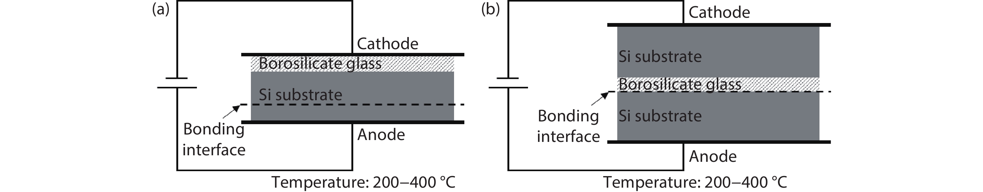
    Fig. 1. Schematic views of (a) silicon–glass anodic bonding and (b) silicon–silicon anodic bonding mediated with a borosilicate glass layer.
    (Color online) (a) Schematic of the DWB process via SiO2 dielectric layers, and (b) shows the IR image of the bonded wafer.
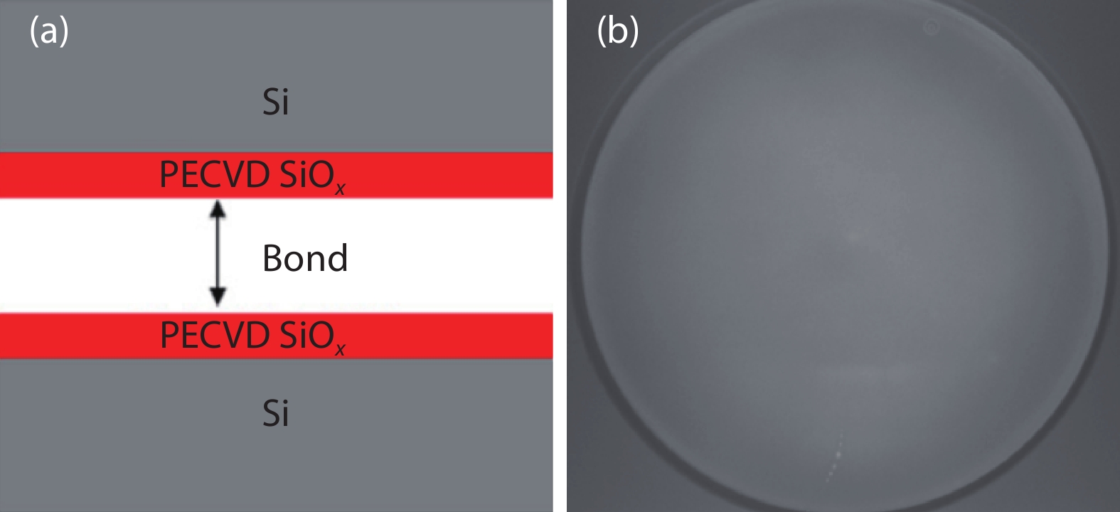
    Fig. 2. (Color online) (a) Schematic of the DWB process via SiO2 dielectric layers, and (b) shows the IR image of the bonded wafer.
    IR images of a bonded wafer with SiO2 dielectric layers (a) as bonded, and (b) after post-bond annealing.
    Fig. 3. IR images of a bonded wafer with SiO2 dielectric layers (a) as bonded, and (b) after post-bond annealing.
    (Color online) (a) Schematic of the bonding process with an additional thin deposited SixNy layer, and the IR images of (b) as-bonded wafers and (c) after post-bond annealing.
    Fig. 4. (Color online) (a) Schematic of the bonding process with an additional thin deposited SixNy layer, and the IR images of (b) as-bonded wafers and (c) after post-bond annealing.
    (Color online) The comparison of FTIR spectral changes at the vibration mode at 3750 cm–1 between the SiOx+ SixNy and SiO2 films after annealing and four-day storage under cleanroom environments.
    Fig. 5. (Color online) The comparison of FTIR spectral changes at the vibration mode at 3750 cm–1 between the SiOx+ SixNy and SiO2 films after annealing and four-day storage under cleanroom environments.
    Change in the SixNy layers stress profile. Compressive stress turns into tensile stress in SixNy layers after annealing, and its stress and bow stay stable after 10 days of storage, indicating that the moisture absorption is blocked.
    Fig. 6. Change in the SixNy layers stress profile. Compressive stress turns into tensile stress in SixNy layers after annealing, and its stress and bow stay stable after 10 days of storage, indicating that the moisture absorption is blocked.
    (Color online) (a) Schematic of AlN to AlN bonding process and the IR images of (b) as-bonded wafers, and (c) after post-bond annealing.
    Fig. 7. (Color online) (a) Schematic of AlN to AlN bonding process and the IR images of (b) as-bonded wafers, and (c) after post-bond annealing.
    (Color online) XPS Atomic concentration profiles of pre-annealed AlN.
    Fig. 8. (Color online) XPS Atomic concentration profiles of pre-annealed AlN.
    (Color online) Schematic of Al2O3 to Al2O3 bonding process.
    Fig. 9. (Color online) Schematic of Al2O3 to Al2O3 bonding process.
    Cross-sectional TEM images of (a) the bonded wafer pair, and (b) the bonding interface.
    Fig. 10. Cross-sectional TEM images of (a) the bonded wafer pair, and (b) the bonding interface.
    (Color online) Schematics of Ge-OI fabrication process.
    Fig. 11. (Color online) Schematics of Ge-OI fabrication process.
    Plan view TEM images of the Ge surface of Ge-OI before and after O2 annealing.
    Fig. 12. Plan view TEM images of the Ge surface of Ge-OI before and after O2 annealing.
    The EPD determined TDD of the Ge of Ge-OI before annealing and after annealing + CMP.
    Fig. 13. The EPD determined TDD of the Ge of Ge-OI before annealing and after annealing + CMP.
    (Color online) Raman spectroscopy of the Ge film on Ge-OI before and after annealing.
    Fig. 14. (Color online) Raman spectroscopy of the Ge film on Ge-OI before and after annealing.
    (Color online) The fabricated 200 mm Ge-OI, GaAs-OI and GaN-OI substrate wafers.
    Fig. 15. (Color online) The fabricated 200 mm Ge-OI, GaAs-OI and GaN-OI substrate wafers.
    (Color online) Schematic flow of the double bonding and layer transfer process.
    Fig. 16. (Color online) Schematic flow of the double bonding and layer transfer process.
    (Color online) (a) Schematic flow of the first bonding process between SOI and thermally oxidized Si handle wafer and (b) IR image of the bonded wafer pair.
    Fig. 17. (Color online) (a) Schematic flow of the first bonding process between SOI and thermally oxidized Si handle wafer and (b) IR image of the bonded wafer pair.
    (Color online) (a) Schematic flow of the first bonding and substrate removal and (b) optical image of the bonded pair after substrate removal where pin-holes are observed.
    Fig. 18. (Color online) (a) Schematic flow of the first bonding and substrate removal and (b) optical image of the bonded pair after substrate removal where pin-holes are observed.
    (Color online) Schematic flow of the double bonding process. (a) IR image of bonded SOI–InGaAs pair and (b) IR image of bonded SOI–GaN pair.
    Fig. 19. (Color online) Schematic flow of the double bonding process. (a) IR image of bonded SOI–InGaAs pair and (b) IR image of bonded SOI–GaN pair.
    (Color online) (a) Schematic flow of 1st bonding with CMP-ed BOX layer. (b) Optical image of the resultant wafer after the process, where pin-holes are observed.
    Fig. 20. (Color online) (a) Schematic flow of 1st bonding with CMP-ed BOX layer. (b) Optical image of the resultant wafer after the process, where pin-holes are observed.
    (Color online) (a) Schematic flow of the double bonding process with additional SiO2 layers. (b) IR image of the bonded wafer pair.
    Fig. 21. (Color online) (a) Schematic flow of the double bonding process with additional SiO2 layers. (b) IR image of the bonded wafer pair.
    (Color online) (a) Schematic flow of double bonding process with BOX layer completely replaced by PECVD oxide. (b) IR image of the bonded pair. No pin-holes are observed.
    Fig. 22. (Color online) (a) Schematic flow of double bonding process with BOX layer completely replaced by PECVD oxide. (b) IR image of the bonded pair. No pin-holes are observed.
    (Color online) IR images and optical images of wafers after double bonding and layer transfer using different methods.
    Fig. 23. (Color online) IR images and optical images of wafers after double bonding and layer transfer using different methods.
    Cross-sectional bright field TEM images of the bonded SOI-Si wafer pairs. (a) The overall view and (b) the bonding interface between PECVD oxide and Si prime wafer.
    Fig. 24. Cross-sectional bright field TEM images of the bonded SOI-Si wafer pairs. (a) The overall view and (b) the bonding interface between PECVD oxide and Si prime wafer.
    (Color online) (a) Updated schematic diagram of the double bonding and layer transfer process. (b) IR image and (c) optical image of the resultant SOI–III–V/Si integrated wafer.
    Fig. 25. (Color online) (a) Updated schematic diagram of the double bonding and layer transfer process. (b) IR image and (c) optical image of the resultant SOI–III–V/Si integrated wafer.
    Cross-sectional TEM image of the Si-CMOS/III–V/Si wafer after double bond and layer transfer.
    Fig. 26. Cross-sectional TEM image of the Si-CMOS/III–V/Si wafer after double bond and layer transfer.
    (Color online) Symmetric (004) reciprocal space map (RSM) of an AlInGaP LED structure measured from XRD (a) before and (b) after bonding with Si-CMOS. Asymmetric (224) RSM of the AlInGaP LED structure (c) before and (d) after bonding with Si-CMOS.
    Fig. 27. (Color online) Symmetric (004) reciprocal space map (RSM) of an AlInGaP LED structure measured from XRD (a) before and (b) after bonding with Si-CMOS. Asymmetric (224) RSM of the AlInGaP LED structure (c) before and (d) after bonding with Si-CMOS.
    (Color online) Schematic flow of replacing Si (111) substrate by Si (001) substrate for GaN HEMT/LED wafer.
    Fig. 28. (Color online) Schematic flow of replacing Si (111) substrate by Si (001) substrate for GaN HEMT/LED wafer.
    IR image of a bonded GaN/Si wafer pair after substrate replacement.
    Fig. 29. IR image of a bonded GaN/Si wafer pair after substrate replacement.
    (Color online) Schematic flow of the diamond CMP process. (a) After oxide deposition, (b) after CMP using slurry with the addition of diamond particles, and (c) another oxide deposition and CMP processes to smoothen the oxide surface which was roughened from the previous step.
    Fig. 30. (Color online) Schematic flow of the diamond CMP process. (a) After oxide deposition, (b) after CMP using slurry with the addition of diamond particles, and (c) another oxide deposition and CMP processes to smoothen the oxide surface which was roughened from the previous step.
    (a) IR image, (b) optical image of Si-CMOS and GaN LED bonded pair on Si (001) substrate.
    Fig. 31. (a) IR image, (b) optical image of Si-CMOS and GaN LED bonded pair on Si (001) substrate.
    (Color online) Schematic of the process flow to realize the GaN LED on quartz substrate. (a) A GaN LED epitaxial film on a Si (111) substrate. (b) First wafer bonding between the GaN LED on Si (111) and a Si handle wafers. (c) Removal of the Si (111) substrate. (d) Deposition of SiO2 and Si3N4 layers. (e) Second wafer bonding between the GaN LED-containing handle and a quartz substrate. (f) GaN LED on quartz substrate is realized by releasing the Si handle wafer.
    Fig. 32. (Color online) Schematic of the process flow to realize the GaN LED on quartz substrate. (a) A GaN LED epitaxial film on a Si (111) substrate. (b) First wafer bonding between the GaN LED on Si (111) and a Si handle wafers. (c) Removal of the Si (111) substrate. (d) Deposition of SiO2 and Si3N4 layers. (e) Second wafer bonding between the GaN LED-containing handle and a quartz substrate. (f) GaN LED on quartz substrate is realized by releasing the Si handle wafer.
    (Color online) (a) IR image of a bonded GaN LED/Si (111) substrate and a Si handle wafer after step Fig. 32(b). (b) Photograph of the GaN LED layers temporarily attached to the Si handle wafer after Si (111) substrate removal, step Fig. 32(c). (c) IR image of the bonded GaN LED layers containing Si handle wafer and a quartz substrate after step Fig. 32(e). (d) Photograph of the GaN LED transferred to the quartz substrate, step Fig. 32(f).
    Fig. 33. (Color online) (a) IR image of a bonded GaN LED/Si (111) substrate and a Si handle wafer after step Fig. 32(b). (b) Photograph of the GaN LED layers temporarily attached to the Si handle wafer after Si (111) substrate removal, step Fig. 32(c). (c) IR image of the bonded GaN LED layers containing Si handle wafer and a quartz substrate after step Fig. 32(e). (d) Photograph of the GaN LED transferred to the quartz substrate, step Fig. 32(f).
    SEM image of the cross-sectional view of the bonded GaN LED on the quartz substrate.
    Fig. 34. SEM image of the cross-sectional view of the bonded GaN LED on the quartz substrate.
    (Color online) Light-up photo of the GaN LED devices on (a) Si and (b) quartz substrates.
    Fig. 35. (Color online) Light-up photo of the GaN LED devices on (a) Si and (b) quartz substrates.
    (Color online) Schematic flow of the multi-bonding and layer transfer process for integration of Si-CMOS and GaAs and GaN together on a common 200 mm Si platform.
    Fig. 36. (Color online) Schematic flow of the multi-bonding and layer transfer process for integration of Si-CMOS and GaAs and GaN together on a common 200 mm Si platform.
    (Color online) IR image of (a) the first bonding between SOI and Si handle wafer, (b) the second bonding between the SOI-handle and the GaAs/Ge/Si substrate, (c) the third bonding between the GaAs/Ge-SOI-handle and the GaN/Si substrate, and (d) optical image of the SOI-GaAs/Ge/GaN/Si substrate after the triple-bond process. The red circle indicates the defects from the backside of the wafer during TMAH etching caused by the poor adhesion of the protective layer, not affecting the bonding quality.
    Fig. 37. (Color online) IR image of (a) the first bonding between SOI and Si handle wafer, (b) the second bonding between the SOI-handle and the GaAs/Ge/Si substrate, (c) the third bonding between the GaAs/Ge-SOI-handle and the GaN/Si substrate, and (d) optical image of the SOI-GaAs/Ge/GaN/Si substrate after the triple-bond process. The red circle indicates the defects from the backside of the wafer during TMAH etching caused by the poor adhesion of the protective layer, not affecting the bonding quality.
    The cross-sectional TEM of the SOI–GaAs/Ge/GaN/Si stack after the triple-bonding and layer transfer process.
    Fig. 38. The cross-sectional TEM of the SOI–GaAs/Ge/GaN/Si stack after the triple-bonding and layer transfer process.
    (Color online) The schematic of Si-CMOS, high frequency GaAs HEMT, and high power GaN PA integrated on a single piece of wafer.
    Fig. 39. (Color online) The schematic of Si-CMOS, high frequency GaAs HEMT, and high power GaN PA integrated on a single piece of wafer.
    Shuyu Bao, Yue Wang, Khaw Lina, Li Zhang, Bing Wang, Wardhana Aji Sasangka, Kenneth Eng Kian Lee, Soo Jin Chua, Jurgen Michel, Eugene Fitzgerald, Chuan Seng Tan, Kwang Hong Lee. A review of silicon-based wafer bonding processes, an approach to realize the monolithic integration of Si-CMOS and III–V-on-Si wafers[J]. Journal of Semiconductors, 2021, 42(2): 023106
    Download Citation