[1] S Deleonibus. Physical and technological limitations of nano CMOS devices to the end of the roadmap and beyond. Eur Phys J Appl Phys, 36, 197(2006).
[2] T Ito, S Okazaki. Pushing the limits of lithography. Nature, 406, 1027(2000).
[3] H S P Wong, D J Frank, P M Solomon et al. Nanoscale CMOS. Proc IEEE, 87, 537(1999).
[4] D H Kim, J A del Alamo. 30 nm E-mode InAs PHEMTs for THz and future logic applications. 2008 IEEE International Electron Devices Meeting, 1(2008).
[5] M Passlack, P Zurcher, K Rajagopalan et al. High mobility III–V MOSFETs for RF and digital applications. 2007 IEEE Int Electron Devices Meet, 621(2007).
[6] R H Kim, D H Kim, J L Xiao et al. Waterproof AlInGaP optoelectronics on stretchable substrates with applications in biomedicine and robotics. Nat Mater, 9, 929(2010).
[7] H Ko, K Takei, R Kapadia et al. Ultrathin compound semiconductor on insulator layers for high-performance nanoscale transistors. Nature, 468, 286(2010).
[8] J Yoon, S Jo, I S Chun et al. GaAs photovoltaics and optoelectronics using releasable multilayer epitaxial assemblies. Nature, 465, 329(2010).
[9] J J Lin, T G You, T T Jin et al. Wafer-scale heterogeneous integration InP on trenched Si with a bubble-free interface. APL Mater, 8, 051110(2020).
[10] J J Lin, T G You, M Wang et al. Efficient ion-slicing of InP thin film for Si-based hetero-integration. Nanotechnology, 29, 504002(2018).
[11] K H Lee, S Bao, E Fitzgerald et al. Integration of III–V materials and Si-CMOS through double layer transfer process. 2014 4th IEEE Int Work Low Temp Bond 3D Integr LTB-3D, 32(2014).
[12] K H Lee, S Y Bao, D Kohen et al. Monolithic integration of III–V HEMT and Si-CMOS through TSV-less 3D wafer stacking. 2015 IEEE 65th Electronic Components and Technology Conference (ECTC), 560(2015).
[13]
[14] Y Q Yan, K Huang, H Y Zhou et al. Wafer-scale fabrication of 42° rotated Y-cut LiTaO3-on-insulator (LTOI) substrate for a SAW resonator. ACS Appl Electron Mater, 1, 1660(2019).
[15] K Huang, Q Jia, T G You et al. Investigation on thermodynamicsof ion-slicing of GaN and heterogeneously integrating high-qualityGaN films on CMOS compatible Si(100) substrates. Sci Rep, 7, 15017.(2017).
[16] A L Yi, Y Zheng, H Huang et al. Wafer-scale 4H-silicon carbide-on-insulator (4H-SiCOI) platform for nonlinear integrated optical devices. Opt Mater, 107, 109990(2020).
[17] D Lei, K H Lee, S Y Bao et al. GeSn-on-insulator substrate formed by direct wafer bonding. Appl Phys Lett, 109, 022106(2016).
[18] W H Xu, Y Wang, T G You et al. First demonstration of waferscale heterogeneous integration of Ga2O3 MOSFETs on SiC and Si substrates by ion-cutting process. 2019 IEEE International Electron Devices Meeting (IEDM), 12.5. 1(2019).
[19] U Gösele, Q Y Tong. Semiconductor wafer bonding. Annu Rev Mater Sci, 28, 215(1998).
[20] Q Y Tong, U Gösele. Semiconductor wafer bonding: Recent developments. Mater Chem Phys, 37, 101(1994).
[21] J B Lasky, S R Stiffler, F R White et al. Silicon-on-insulator (SOI) by bonding and ETCH-back. 1985 Int Electron Devices Meet, 684(1985).
[22] A Plößl. Wafer direct bonding: Tailoring adhesion between brittle materials. Mater Sci Eng R, 25, 1(1999).
[23] K T Turner, S M Spearing. Modeling of direct wafer bonding: Effect of wafer bow and etch patterns. J Appl Phys, 92, 7658(2002).
[24] S Taniyama, Y H Wang, M Fujino et al. Room temperature wafer bonding using surface activated bonding method. 2008 IEEE 9th VLSI Packag Work Jpn, 141(2008).
[25] H Takagi, K Kikuchi, R Maeda et al. Surface activated bonding of silicon wafers at room temperature. Appl Phys Lett, 68, 2222(1996).
[26] M M R Howlader, T Watanabe, T Suga. Investigation of the bonding strength and interface current of p-Si/n-GaAs wafers bonded by surface activated bonding at room temperature. J Vac Sci Technol B, 19, 2114(2001).
[27] T R Chung, L Yang, N Hosoda et al. Room temperature GaAs–Si and InP–Si wafer direct bonding by the surface activated bonding method. Nucl Instrum Methods Phys Res B, 121, 203(1997).
[28] H Takagi, J Utsumi, M Takahashi et al. Room-temperature bonding of oxide wafers by Ar-beam surface activation. ECS Trans, 16, 531(2019).
[29] S Essig, O Moutanabbir, A Wekkeli et al. Fast atom beam-activated n-Si/n-GaAs wafer bonding with high interfacial transparency and electrical conductivity. J Appl Phys, 113, 203512(2013).
[30] A P Hinterreiter, B Rebhan, C Flötgen et al. Surface pretreated low-temperature aluminum-aluminum wafer bonding. Microsyst Technol, 24, 773(2018).
[31]
[32] N Malik, K Schjølberg-Henriksen, E Poppe et al. AlAl thermocompression bonding for wafer-level MEMS sealing. Sens Actuators A, 211, 115(2014).
[33] C H Tsau, S M Spearing, M A Schmidt. Fabrication of wafer-level thermocompression bonds. J Microelectromechan Syst, 11, 641(2002).
[34] D H Xu, E R Jing, B Xiong et al. Wafer-level vacuum packaging of micromachined thermoelectric IR sensors. IEEE Trans Adv Packag, 33, 904(2010).
[35] J Fan, D F Lim, C S Tan. Effects of surface treatment on the bonding quality of wafer-level Cu-to-Cu thermo-compression bonding for 3D integration. J Micromech Microeng, 23, 045025(2013).
[36] K N Chen, A Fan, R Reif. Microstructure examination of copper wafer bonding. J Electron Mater, 30, 331(2001).
[37] K Gao, Q Y Zhang, W G Su et al. Patterned Al–Ge wafer bonding for reducing in-process side leakage of eutectic. 2018 IEEE 13th Annual International Conference on Nano/Micro Engineered and Molecular Systems (NEMS), 332(2018).
[38] Y S Tang, H C Chen, Y T Kho et al. Investigation and optimization of ultrathin buffer layers used in Cu/Sn eutectic bonding. IEEE Trans Compon Packag Manuf Technol, 8, 1225(2018).
[39] R F Wolffenbuttel. Low-temperature intermediate Au-Si wafer bonding; eutectic or silicide bond. Sens Actuators A, 62, 680(1997).
[40] Y T Cheng, n L Lin, K Najafi. Localized silicon fusion and eutectic bonding for MEMS fabrication and packaging. J Microelectromechan Syst, 9, 3(2000).
[41]
[42] D L Li, Z G Shang, Y She et al. Investigation of Au/Si eutectic wafer bonding for MEMS accelerometers. Micromachines, 8, 158(2017).
[43] U M Mescheder, M Alavi, K Hiltmann et al. Local laser bonding for low temperature budget. Sens Actuators A, 97/98, 422(2002).
[44] R Knechtel. Glass frit bonding: An universal technology for wafer level encapsulation and packaging. Microsyst Technol, 12, 63(2005).
[45] G Q Wu, D H Xu, B Xiong et al. Wafer-level vacuum packaging for MEMS resonators using glass frit bonding. J Microelectromechan Syst, 21, 1484(2012).
[46] R Tian, F Cao, Y Li et al. Application of laser-assisted glass frit bonding encapsulation in all inorganic quantum dot light emitting devices. Mol Cryst Liq Cryst, 676, 59(2018).
[47] F Niklaus, P Enoksson, E Kalvesten et al. Low-temperature full wafer adhesive bonding. J Micromechan Microeng, 11, 100(2001).
[48] V Dragoi, T Glinsner, G Mittendorfer et al. Adhesive wafer bonding for MEMS applications. Proc SPIE 5116, Smart Sensors, Actuators, and MEMS, 5116, 160(2003).
[49] S J Bleiker, V Dubois, S Schröder et al. Adhesive wafer bonding with ultra-thin intermediate polymer layers. Sens Actuators A, 260, 16(2017).
[50] F Niklaus, G Stemme, J Q Lu et al. Adhesive wafer bonding. J Appl Phys, 99, 031101(2006).
[51] F Niklaus, P Enoksson, E Kälvesten et al. A method to maintain wafer alignment precision during adhesive wafer bonding. Sens Actuators A, 107, 273(2003).
[52] F Niklaus, R J Kumar, J J McMahon et al. Adhesive wafer bonding using partially cured benzocyclobutene for three-dimensional integration. J Electrochem Soc, 153, G291(2006).
[53]
[54] H Henmi, S Shoji, Y Shoji et al. Vacuum packaging for microsensors by glass-silicon anodic bonding. Sens Actuators A, 43, 243(1994).
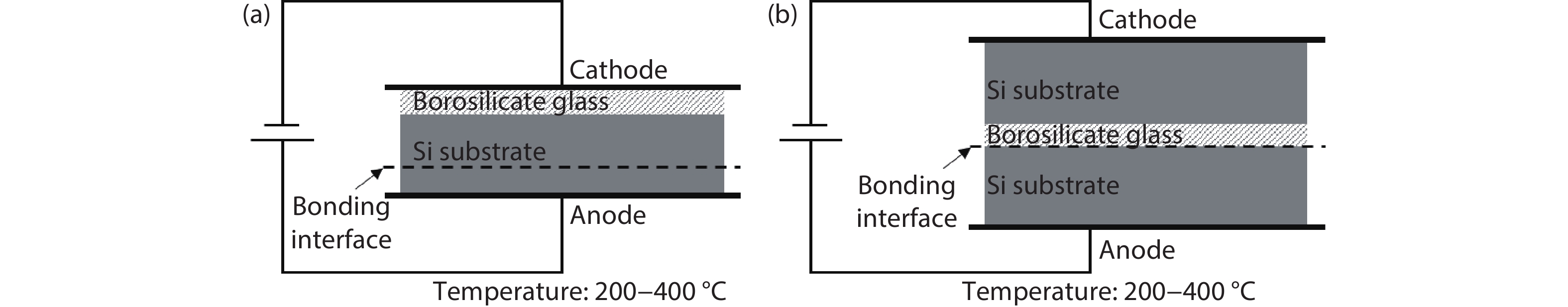
[55] A Hanneborg, M Nese, P Ohlckers. Silicon-to-silicon anodic bonding with a borosilicate glass layer. J Micromech Microeng, 1, 139(1991).
[56] T M H Lee, I M Hsing, C Y N Liaw. An improved anodic bonding process using pulsed voltage technique. J Microelectromechan Syst, 9, 469(2000).
[57] M A Schmidt. Wafer-to-wafer bonding for microstructure formation. Proc IEEE, 86, 1575(1998).
[58] Q Y Tong, U Gösele. A model of low-temperature wafer bonding and its applications. J Electrochem Soc, 143, 1773(2019).
[59] K H Lee, S Y Bao, Y Wang et al. Suppression of interfacial voids formation during silane (SiH4)-based silicon oxide bonding with a thin silicon nitride capping layer. J Appl Phys, 123, 015302(2018).
[60] S Bao, K H Lee, G Y Chong et al. AlN–AlN layer bonding and its thermal characteristics. ECS J Solid State Sci Technol, 4, P200(2015).
[61] S Y Bao, K H Lee, C Wang et al. Germanium-on-insulator virtual substrate for InGaP epitaxy. Mater Sci Semicond Process, 58, 15(2017).
[62] K H Lee, S Y Bao, G Y Chong et al. Fabrication and characterization of germanium-on-insulator through epitaxy, bonding, and layer transfer. J Appl Phys, 116, 103506(2014).
[63] K H Lee, S Y Bao, G Y Chong et al. Fabrication of germanium-on-insulator (GOI) with improved threading dislocation density (TDD) via buffer-less epitaxy and bonding. 2014 7th Int Silicon-Ger Technol Device Meet ISTDM, 51(2014).
[64] K H Lee, S Y Bao, G Y Chong et al. Defects reduction of Ge epitaxial film in a germanium-on-insulator wafer by annealing in oxygen ambient. APL Mater, 3, 016102(2015).
[65] K H Lee, C S Tan, Y Wang et al. Monolithic integration of Si-CMOS and III–V-on-Si through direct wafer bonding process. IEEE J Electron Devices Soc, 6, 571(2018).
[66] K H Lee, L Zhang, B Wang et al. Integration of Si-CMOS and III–V materials through multi-wafer stacking. 2017 IEEE SOI-3D-Subthreshold Microelectronics Technology Unified Conference (S3S), 1(2017).
[67] K H Lee, Y Wang, L Zhang et al. GaN LED on quartz substrate through wafer bonding and layer transfer processes. ECS Trans, 86, 31(2018).
[68]
[69] K H Lee, S Y Bao, L Zhang et al. Integration of GaAs, GaN, and Si-CMOS on a common 200 mm Si substrate through multilayer transfer process. Appl Phys Express, 9, 086501(2016).