
Shuyu Bao, Yue Wang, Khaw Lina, Li Zhang, Bing Wang, Wardhana Aji Sasangka, Kenneth Eng Kian Lee, Soo Jin Chua, Jurgen Michel, Eugene Fitzgerald, Chuan Seng Tan, Kwang Hong Lee. A review of silicon-based wafer bonding processes, an approach to realize the monolithic integration of Si-CMOS and III–V-on-Si wafers[J]. Journal of Semiconductors, 2021, 42(2): 023106
- Journal of Semiconductors
- Vol. 42, Issue 2, 023106 (2021)
Abstract
1. Introduction
The silicon (Si) complementary metal–oxide–semiconductor (CMOS) is the most dominant component in the semiconductor industry and the miniaturization of Si-CMOS is the main trend to further improve its speed, power consumption and production cost[
The performance improvement of a transistor is driven by the carrier mobility enhancement in the channel. The Group IV materials, such as SiGe and Ge, and the Group III–V compound materials, such as GaAs and InP, are well-known for their unique electrical properties and superior high mobility transistors[
Epitaxial integration of growing III–V materials directly on Si substrates is the most desirable approach to integrate the III–V transistor with the Si platform. However, this method experiences many issues due to the large lattice mismatch and the difference in coefficient of thermal expansion (CTE) between the III–V compound semiconductor and Si. Thus, it remains a challenge to form thin III–V layers on Si while retaining excellent crystal quality. In addition, the growth of III–V materials requires a high temperature condition (650–1350 °C, depending on the materials systems).
Compared to the epitaxial integration method, direct wafer bonding (DWB) is a more straightforward and practical approach to achieve the heterogeneous integration between III–V and the Si substrate without the exposure of Si-CMOS to high temperature[
In Section 2 of this paper, several mainstream bonding techniques, including their applications and challenges, will be reviewed. In Section 3, our recent progress of single-, double- and multi-DWB bonding techniques will be discussed in detail. After that, various applications enabled by these techniques, such as CMOS-driven HEMT, LED, and other novel applications will be shown at the end of this paper.
2. Wafer bonding techniques
In this section, various mainstream approaches in wafer-scale bonding will be reviewed, including DWB, surface-activated bonding, thermocompression bonding, eutectic bonding, glass frit bonding, adhesive bonding and anodic bonding. Among these bonding techniques, the DWB is the most promising approach for wafer-scale III–V on Si integration and Si-CMOS integrated devices due to its strong bonding strength, reliable bonding interface and low temperature processing conditions. This section will present these bonding techniques in more details.
2.1. Direct wafer bonding
Heterogeneous integration technologies show great potential in the applications of novel materials, MEMS devices and 3D packaging. In the past, wire bonding, flip-chip and epitaxial integration were commonly used for heterogeneous integrations. However, due to the concerns of process complexity, scalability and materials quality, these integration applications were ruled out by the traditional materials science and semiconductor processing technology[
Besides annealing and plasma treatment, there are some stringent requirements in the process flow to ensure a successful wafer bonding, such as bonding energy, surface cleanliness, roughness and flatness. Firstly, the bonding is initiated by applying a physical force at one point on the wafer, allowing the bond front to propagate. The propagation of the bond front to a sealed interface is dependent on the balance between the surface energy dissipation to form the bond and the strain energy to deform the wafers[
When the wafers are bonded, bonding defects may exist, causing the failures of device fabrication in the later processing steps. Therefore, it is important to detect these bonding defects at early stages. One of the most commonly used methods is the IR imaging. As silicon is transparent at IR wavelength range (> 1.1
2.2. Surface activated bonding (SAB)
In SAB, the bonding reaction is driven by the cohesive and adhesive energy of solids. Wafer surfaces are sputter-cleaned and activated with argon fast atom beam (FAB) before being brought into close contact in an ultrahigh vacuum (~10−5–10−6 Pa) chamber. Then, large bonding pressure of a few tens of mega-pascal is applied to the close-contacted wafer pair. The bonding strength achievable at room temperature is close to the bulk fracture energy of the materials[
2.3. Thermocompression bonding
Thermocompression bonding, also known as diffusion bonding, is a metal-based bonding technique that brings two surfaces into atomic contact under heat and pressure. A smooth surface with high surface flatness is desirable as it promotes the interatomic attractions. Metals with a high diffusion rate are used in this bonding technique. The most commonly used metals are Au, Al and Cu[
2.4. Eutectic bonding
Eutectic wafer bonding is a widespread method in MEMS systems for hermetically sealed packaging and 3D integrations. Compared to thermocompression bonding between two metals, eutectic bonding is based on a eutectic system of alloys used as the intermediate bonding layer to bond two wafers together via diffusion mechanism. In the eutectic system, their mixture can melt or solidify at a lower temperature than the melting point of the individual component materials. There is a wide range of material combinations for eutectic wafer bonding, such as Au–In, Au–Ge, Au–Sn, Au–Si, Al–Ge and Cu–Sn[
2.5. Glass frit bonding
Glass frit bonding is a wafer-level encapsulation and packaging technology. It allows strong hermetic wafer bonds with a high process yield, especially designed for MEMS resonators and micosensors[
2.6. Adhesive bonding
Adhesive bonding utilizes polymer adhesives such as benzocyclobutene (BCB), spin-on glass (SOG), resists and polyimides as the intermediate layer for bonding[
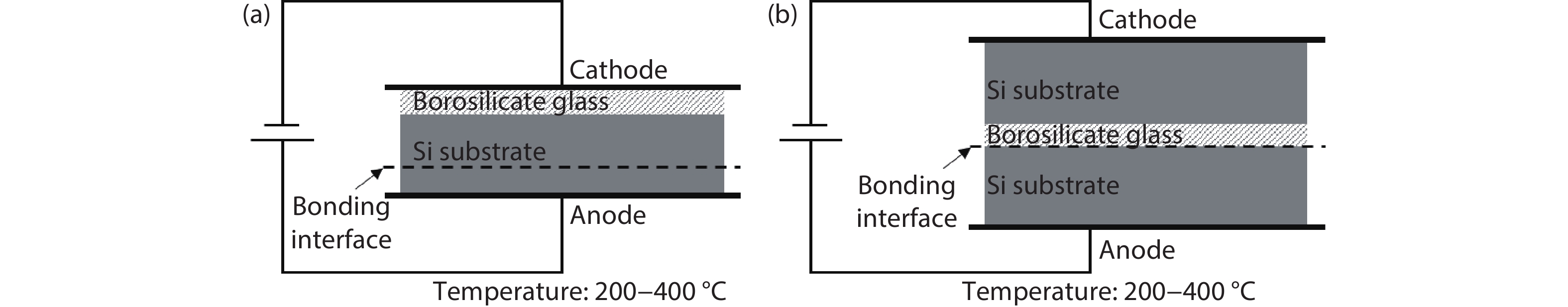
2.7. Anodic bonding
Anodic bonding, also referred to as field assisted bonding or electrostatic bonding, joins ion conductive materials to metal or silicon through a sufficiently strong electrical field[
![]()
Figure 1.Schematic views of (a) silicon–glass anodic bonding and (b) silicon–silicon anodic bonding mediated with a borosilicate glass layer.
3. Wafer bonding technique and applications
Our group has successfully demonstrated the monolithic integration of Si-CMOS on SOI and III–V device layers on Si using wafer bonding and layer transfer techniques. In this section, we will discuss various DWB techniques, such as single-, double- and multiple-bonding techniques, and their possible applications. Since the high temperature growth of III–V wafers can be completed without the presence of Si-CMOS layers, DWB provides more temperature tolerance to pre-bonding processes. In addition, a plasma activation step is used to increase the surface hydrophilicity of bonding dielectric layers, and it can be performed at room temperature and atmosphere pressure. Therefore, DWB also avoids the thermal damage to Si-CMOS devices during the bonding processes.
3.1. Direct wafer bonding using various types of bonding dielectrics
3.1.1. SiO2 to SiO2 bonding
Silicon oxide (SiO2) is a widely used dielectric material in the semiconductor industry, deposited by plasma-enhanced chemical vapor deposition (PECVD). In this experiment, two Si wafers were pre-cleaned using standard RCA to remove organic and metallic contaminants, followed by the deposition of SiO2 by PECVD. Then additional densification was applied to remove the gas molecules or by-product residuals. After densification, the oxide surface was polished by CMP to smoothen the oxide surface to obtain a nearly atomically flat surface. After an RCA-based post-CMP cleaning step, a particle-free hydrophilic surface was obtained. By bringing two wafers into intimate contact at room temperature, the wafers were bonded. Fig. 2(a) shows the schematic of this bonding process, and Fig. 2(b) shows the IR image of the bonded wafers. An annealing step at 300 °C was applied after bonding to enhance the bonding strength[
![]()
Figure 2.(Color online) (a) Schematic of the DWB process via SiO2 dielectric layers, and (b) shows the IR image of the bonded wafer.
However, as shown in Fig. 3, there are many voids after post-bond annealing. These voids are caused by the increased incorporation of hydroxyl groups (–OH) during annealing, which can be explained by the silanol polymerization reaction. During this reaction, Si–OH groups react with each other and form Si–O–Si groups and H2O, as expressed by the following formula[
![]()
Figure 3.IR images of a bonded wafer with SiO2 dielectric layers (a) as bonded, and (b) after post-bond annealing.
The H2O and absorbed moisture can be trapped and accumulated at the bonding interface to form voids.
3.1.2. Si3N4 to Si3N4 bonding
To address the void formation issue after post-bond annealing, an additional thin SixNy layer a capping layer was added to SiO2 layers by PECVD, as shown in Fig. 4(a)[
![]()
Figure 4.(Color online) (a) Schematic of the bonding process with an additional thin deposited Si
The IR images of the as-bonded and post-bond annealing wafers pairs with SixNy intermediate layers are shown Figs. 4(b) and 4(c).
To verify the function of the additional nitride layer, Fourier transform infrared (FTIR) spectra were used. From Fig. 5, the vibration mode at 3750 cm−1 for the wafers with nitride films stays almost flat after four days of storage compared to the wafer with SiO2 film only, indicating the capping nitride layer was acting as a moisture barrier.
![]()
Figure 5.(Color online) The comparison of FTIR spectral changes at the vibration mode at 3750 cm–1 between the SiO
The film stress can be determined by using a stress measurement system, it shows that the compressive stress in SixNy layers becomes tensile stress, and the tensile stress is very stable after 10 days of storage, as shown in Fig. 6. This also indicates that the SixNy layers block the moisture absorption after annealing. This can be explained by the higher density and mechanical strength, compared to SiO2.
![]()
Figure 6.Change in the Si
3.1.3. AlN to AlN bonding
AlN can also be used as the bonding dielectric, due to its excellent properties, such as good temperature stability and high thermal conductivity (AlN: 134 Wm−1K−1 and SiO2: 1.4 Wm−1K−1). Similar to SiO2 to SiO2 bonding, two Si wafers were pre-cleaned, followed by the deposition of 20 nm AlN films by sputtering aluminium in N2 atmosphere at 75 °C using atomic layer deposition (ALD)[
![]()
Figure 7.(Color online) (a) Schematic of AlN to AlN bonding process and the IR images of (b) as-bonded wafers, and (c) after post-bond annealing.
During the pre-annealing step for outgassing in a furnace, the AlN thin film was prone to oxidation when exposed to ambient, and the high temperature at 450 °C also accelerated the oxidation. With this concern, the composition of AlN thin films was verified by XPS measurement. Fig. 8 shows the atomic concentration against the sputtering depth. The atomic ratio of Al and N are close to 1 : 1, indicating the expected composition of AlN. The surface region shows a slight stoichiometry mismatch, which is possibly caused by the partial oxidation by H2O or O2 in the air.
![]()
Figure 8.(Color online) XPS Atomic concentration profiles of pre-annealed AlN.
3.1.4. Al2O3 to Al2O3 bonding
We also investigated Al2O3 as the bonding dielectric[
![]()
Figure 9.(Color online) Schematic of Al2O3 to Al2O3 bonding process.
After bonding, the post-bond annealing at 300 °C in an atmospheric N2 ambient for 3 h was performed for bond enhancement.
Fig. 10 shows a cross-section transmission electron microscope (TEM) image of the bonded wafer pair to verify the bonding quality at the Al2O3 bonding interface. As shown in the TEM images, the Al2O3 bonding interface is uniform and seamless with no sign of micro-voids. In addition, the O2 plasma activation modified the stoichiometry of the Al2O3, causing contrast differences in the Al2O3 layers.
![]()
Figure 10.Cross-sectional TEM images of (a) the bonded wafer pair, and (b) the bonding interface.
3.1.5. Applications (‘X’-OI)
Silicon-on-insulator (SOI) has many advantages over Si, such as reduced parasitic capacitances and short channel effects. Similar to SOI, the germanium-on-insulator (Ge-OI) and other III–V materials-on-insulator (‘X’-OI) are not only used as the substrates, but also as active layers, such as the light source in a silicon photonic system. In addition, since Si is the handle wafer, some of the CMOS tools and processes can be shared with these new insulators.
In this section, we present a scalable method to fabricate high-quality Ge-OI wafers[
In the Ge-OI fabrication experiment, two sets of wafers were prepared: (i) Ge films epitaxially grown on 200 mm Si donor wafer using a metal organic vapor deposition (MOCVD), and (ii) Si (001) handle wafer. A 10 nm thin Al2O3 layer was deposited on each prepared wafer by ALD.
The bonding process was similar to Al2O3 to Al2O3 bonding as described previously. SiO2 can be used as the bonding dielectric as well. After bonding and post-bond annealing, the donor Si substrate was removed through mechanical grinding and selective wet etching in 80 °C tetramethylammonium hydroxide (TMAH) solution, which etch-stopped at the Ge layer. The backside of the handle wafer was protected with spin-coated ProTEK® B3-25 films during TMAH etching. Then the O2 plasma with the power of 800 W was applied to remove the protective coating. The schematic of the Ge-OI fabrication process flow is shown in Fig. 11.
![]()
Figure 11.(Color online) Schematics of Ge-OI fabrication process.
The Ge-OI substrate was annealed at 850 °C in O2 environment for 4 h, followed by CMP process, to reduce the misfit dislocation by oxidation, and the threading dislocation densities (TDDs) by annihilation. After that, HF etching (49% HF : H2O = 1 : 20, by volume) for 30 s to remove the oxidized Ge layer, a Ge film with a low TDD of mid-106 cm–2 was achieved. This TDD level of the Ge is good enough for the Ge film is good enough for most electronic and optoelectronic device applications.
TEM and etch-pit density (EPD) methods were used to characterize the Ge film quality. Plan view TEM shows the Ge-OI surface before and after O2 annealing, as shown in Fig. 12. It shows that the TDD was reduced by 1 order of magnitude after annealing. As EPD is a fast and cheap method, it was used to quantify the TDD of the Ge film after annealing and CMP by etching the sample in iodine solution for 1 s. As shown in Fig. 13, the EPD counted TDD was reduced by two orders of magnitudes from (5.2 ± 0.45) × 108 to (2.5 ± 0.4) × 106 cm–2 after annealing and CMP.
![]()
Figure 12.Plan view TEM images of the Ge surface of Ge-OI before and after O2 annealing.
![]()
Figure 13.The EPD determined TDD of the Ge of Ge-OI before annealing and after annealing + CMP.
To determine the alloy composition and strain of the Ge film, Raman spectroscopy was used. As shown in Fig. 14, there was no signal of the Si–Si vibration mode as the Si from the donor wafer was removed completely by TMAH. After O2 annealing, the signal of the Si–Ge vibration mode disappeared as the Si/Ge intermixed layer was removed. The inset figure shows a blue shift of the Ge–Ge vibration peak from 296 to 302 cm−1 after O2 annealing, indicating the Ge film of the Ge-OI was nearly stress-free after annealing. This may due to the amorphous nature of Al2O3 layer which acts as a stress-free buffer. Also, the Si and Ge/Si intermixed layer were removed by etching and subsequent O2 annealing, therefore Ge is no longer constrained by Si, which led to a nearly stress-free state.
![]()
Figure 14.(Color online) Raman spectroscopy of the Ge film on Ge-OI before and after annealing.
GaAs-OI and GaN-OI substrate can also be fabricated through similar bonding processes as shown in Fig. 15. Depending on applications, various bonding dielectrics (SiO2, Al2O3 or AlN) can be chosen.
![]()
Figure 15.(Color online) The fabricated 200 mm Ge-OI, GaAs-OI and GaN-OI substrate wafers.
In summary, the ‘X’-OI substrate can be fabricated through buffer-less III–V epitaxy, bonding and layer transfer. This method is scalable to various wafer sizes and makes the CMOS devices with III–V/Si integration on common Si wafers become possible.
3.2. Double bonding and layer transfer for Si-CMOS and III–V/Si integration
With the optimized bonding processes as described previously, in this section, we demonstrate a method to integrate III–V compound semiconductor materials with SOI-CMOS on a common Si substrate[
In this experiment, three sets of wafers were prepared: (i) p-type 200 mm Si (001) prime-grade wafers (as Si handle wafer), (ii) patterned silicon-on-insulator (SOI) wafer, with Si and buried oxide (BOX, thermal SiO2), and (iii) III–V on Si wafer (e.g., InGaAs/GaAs/Ge-on-Si or GaN-on-Si) wafers. The schematic flow diagram of the process is shown in Fig. 16.
![]()
Figure 16.(Color online) Schematic flow of the double bonding and layer transfer process.
3.2.1. First bonding (between SOI wafer and thermal oxidized Si handle)
The first bonding was between the patterned SOI wafer and thermally oxidized Si handle wafer. The bonding quality was justified using the IR camera, where any interface voids formed between the bonded wafer pair can be observed. As shown in Fig. 17, no significant voids or particles are observed from the IR image, which indicates an excellent bonding quality between the SOI wafer and thermally oxidized Si handle wafer.
![]()
Figure 17.(Color online) (a) Schematic flow of the first bonding process between SOI and thermally oxidized Si handle wafer and (b) IR image of the bonded wafer pair.
After the first bonding, the Si from the SOI-CMOS donor wafer was ground down to 50 μm, followed by TMAH chemical etching to completely remove the remaining Si, which etched stopped at the BOX layer. However, the BOX layer is slightly damaged by the TMAH solution, and a lot of pin-holes are formed and can be observed, as shown in Fig. 18. We believed that this could be due to the slight etching on the sub-standard quality BOX, where the thermal oxide of the BOX is grown using relatively low-quality wet oxidation instead of higher quality dry oxidation.
![]()
Figure 18.(Color online) (a) Schematic flow of the first bonding and substrate removal and (b) optical image of the bonded pair after substrate removal where pin-holes are observed.
After the first layer transfer, the SOI-CMOS is now on the Si handle wafer. The second bonding is performed between the patterned SOI and III–V/Si wafer. The IR images of the InGaAs and GaN are shown in Fig. 19. Unbounded areas are observed due to pin-holes on the BOX layer. In addition, the particles from the III–V/Si may also contribute to the unbounded area.
![]()
Figure 19.(Color online) Schematic flow of the double bonding process. (a) IR image of bonded SOI–InGaAs pair and (b) IR image of bonded SOI–GaN pair.
3.2.2. Replacement of the BOX layer with PECVD oxide
To tackle the pin-holes issue associated with the BOX layer, the BOX surface was planarized by CMP process. Right after the CMP step, RCA-based cleaning was carried out, followed by a de-ionized (DI) water rinse and spin dry using spin rinse dryer (SRD). However, the pin-hole problem became more obvious and was worse after the CMP process, as shown in Fig. 20.
![]()
Figure 20.(Color online) (a) Schematic flow of 1st bonding with CMP-ed BOX layer. (b) Optical image of the resultant wafer after the process, where pin-holes are observed.
The next attempt to address the pin-hole problem was to use an additional 50 nm SiO2 deposited by plasma-enhanced CVD (PECVD), as a compensation layer on top of the BOX layer. The addition of the PECVD oxide roughens the oxide surface, which prevents a successful wafer bonding in the subsequent step. Therefore, after the PECVD oxide, densification was carried out and followed by the CMP process to planarize the oxide surface. However, after the second bonding, there are still many unbonded areas observed in the bonded wafer pair, as shown in Fig. 21.
![]()
Figure 21.(Color online) (a) Schematic flow of the double bonding process with additional SiO2 layers. (b) IR image of the bonded wafer pair.
Then the third attempt to avoid the pin-holes problem was to remove the BOX layer completely and replace it with PECVD oxide. The sub-standard quality BOX layer was removed by diluted HF solution (with volume ratio HF : H2O = 1 : 10), and followed by PECVD oxide deposition. CMP was carried out to smoothen the PECVD oxide for the second bonding process. Then, the wafer with the PECVD oxide was bonded to another Si prime wafer (no III–V layers). The bonding quality is verified with the IR image. No significant void is observed, as shown in Fig. 22.
![]()
Figure 22.(Color online) (a) Schematic flow of double bonding process with BOX layer completely replaced by PECVD oxide. (b) IR image of the bonded pair. No pin-holes are observed.
3.2.3. Second bonding (between SOI-handle pair and Si prime wafer)
The second bonding was performed between the SOI-handle pair and a Si prime wafer. The Si handle wafer was then completely removed by grinding and chemical etching. With the CMP-on-BOX method, after the double bonding and layer transfer process, delamination is observed on the surface of the bonded SOI–Si wafer. The delamination area is corresponding to the un-bonded area due to the pin-hole issue. A similar delamination issue is also expected for the PECVD-oxide-on-BOX method. By completely removing the BOX layer and replacing it with PECVD oxide, a clean surface with an almost defect-free SOI–Si wafer pair is successfully demonstrated after the second bonding and removal of the handle wafer.
Fig. 23 (the top row) shows a comparison after the second bonding. For the CMP-on-BOX method, unbonded areas are observed across the entire wafer. Many unbonded areas can be observed for the PECVD SiO2 (-on-BOX) method as well. Almost defect-free wafer is observed for the BOX etching method.
![]()
Figure 23.(Color online) IR images and optical images of wafers after double bonding and layer transfer using different methods.
The Si handle wafer was then removed by mechanical grinding and wet chemical etching as described previously. Film peeling was observed from the SOI–Si wafer as shown in Fig. 23 (the bottom row). The delaminated area is even larger than the unbounded area before Si handle removal, due to the weak bonding strength around the unbounded area, which leads to easier film delamination when the handle wafer is released.
Cross-sectional TEM is used to exam the quality of SOI–Si bonding interface after double bonding and layer transfer process using BOX etching method, as shown in Fig. 24. The bonding interface between PECVD oxide and Si prime wafer are smooth and uniform, with no significant micro-voids are observed in the field of view. Therefore, a seamless bonding at the microscale level with the PECVD-oxide-only method has been successfully achieved.
![]()
Figure 24.Cross-sectional bright field TEM images of the bonded SOI-Si wafer pairs. (a) The overall view and (b) the bonding interface between PECVD oxide and Si prime wafer.
3.2.4. Applications: Bonding approach for Si-CMOS + III–As/P or III–N HEMT/LED wafers
We use the same process flow as described previously to demonstrate the integration of Si-CMOS + III–As/P HEMT or LED wafer. Now the actual Si-CMOS devices wafer and the III–As/P with device layers are used instead of the prime Si wafer. Therefore, the second bonding Si3N4 to Si3N4 bonding discussed in the previous section will be used. The updated schematic flow is shown in Fig. 25 below.
![]()
Figure 25.(Color online) (a) Updated schematic diagram of the double bonding and layer transfer process. (b) IR image and (c) optical image of the resultant SOI–III–V/Si integrated wafer.
Three sets of 200 mm wafers were prepared for this experiment: (i) Si (001) wafers, (ii) Si-CMOS/SOI wafers that have undergone front-end-of-line (FEOL) processing only in Si foundries, (iii) InGaAs HEMT or AlInGaP LED epitaxial films which were grown directly on GaAs/Ge/Si (001) wafers with 6° off-cut toward the [110] direction by MOCVD.
The Si-CMOS/SOI wafer was first deposited with 500 nm PECVD SiO2 layer, followed by densification process in N2 environment to eliminate the residual gas molecules and by-products incorporated into the layer during oxide deposition. Then the oxide surface was planarized by chemical mechanical planarization (CMP). Before the first bonding, both the SOI wafer and Si handle wafers were subjected to O2 plasma exposure to increase the surface hydrophilicity. Then both wafers were rinsed with de-ionized (DI) water and spin-dried to clean the wafers and to populate the surface with hydroxyl (–OH) groups at a sufficiently high density to initiate wafer bonding. The post-bonding was performed at 300 °C in an atmospheric pressure N2 ambient for 3 h to further increase the bond strength. The Si substrate from the SOI wafer was then completely removed by mechanical grinding and wet chemical etching in trtramethylammonium hydroxide (TMAH) solution, to realize the first layer transfer.
For the second bonding and layer transfer process, the BOX layer was first removed in HF solution and replaced with PECVD oxide, followed by densification and planarization, and additional PECVD Si3N4 (with densification) layer deposition, to address the pin-holes and outgassing issues. Then, the III–V/Si wafers (InGaAs HEMT, AlGaInP LED epitaxial films on Si) were also subjected to the same PECVD oxide and nitride deposition processes. After that, the two sets of wafer pairs were bonded together, followed by Si handle release to realize the Si-CMOS/III–V on Si wafer.
The cross-sectional TEM image in Fig. 26 shows the stack of Si-CMOS + InGaP LED on a common Si platform. A smooth and clean bonding interface can be observed with no micro-voids between two PECVD Si3N4 layers. A uniform and seamless bonding at the microscale level is successfully demonstrated.
![]()
Figure 26.Cross-sectional TEM image of the Si-CMOS/III–V/Si wafer after double bond and layer transfer.
Non-destructive X-ray diffraction (XRD) measurements were used to characterize the properties of the AlInGaP LED wafer before and after the bonding process. There is no significant change in the peak positions and full widths at half maximum (FWHMs) of the active p-AlGaInP and n-AlGaInP layers, as well as the Ge + GaAs buffer layers, as shown in the reciprocal space map (RSM) from Fig. 27. This confirms that the bonding process does not significantly compromise the film quality.
![]()
Figure 27.(Color online) Symmetric (004) reciprocal space map (RSM) of an AlInGaP LED structure measured from XRD (a) before and (b) after bonding with Si-CMOS. Asymmetric (224) RSM of the AlInGaP LED structure (c) before and (d) after bonding with Si-CMOS.
Similar double bonding and layer transfer process described above was also applied for the integration of Si-CMOS + III–N (e.g., GaN) HEMT or LED wafers. However, due to the high-temperature MOCVD grown GaN on Si (111) wafers, the Si-CMOS + GaN HEMT/LED transfer yield is only ~50%.
This is mainly because during the high temperature GaN growth, slip lines formed at the wafer edge which propagated towards the center of the wafer weakens the Si (111) wafer and makes the wafer brittle. In addition, for the direct epitaxially grown GaN-on-Si wafer, the AlGaN buffer layers and GaN layers contribute different levels of stress and build up the stress levels on the Si (111) substrate which ultimately makes the Si substrate even more fragile.
Although minimizing the radical temperature difference across the Si (111) wafer during the III–N growth will reduce the slip line formation and improve the wafer fragility, it is impossible to fully eliminate vertical temperature differences through the wafer during the growth. In our MOCVD reactor, because the heating is only performed from the backside of the wafer. Thus, to address this issue, we introduced an additional wafer bonding and layer transfer processes, to replace the fragile Si (111) substrate by a new Si (001) substrate, the process flow of this substrate replacement is shown in Fig. 28.
![]()
Figure 28.(Color online) Schematic flow of replacing Si (111) substrate by Si (001) substrate for GaN HEMT/LED wafer.
First, a PECVD SiO2 layer was deposited onto the III–N HEMT/LED on the Si (111) (donor 1) wafer, followed by densification and CMP processes. Then, a Si (001) (donor 2) wafer was bonded to the III–N HEMT/LED wafer, followed by post-bonding annealing. After that, the Si (111) (donor 1) substrate was completely removed through a combination of mechanical grinding and wet-chemical etching in HNA solution (hydrofluoric + nitric + acetic acids). The bonded wafer and a new Si (001) (carrier) substrate were then subject to PECVD SiO2 deposition, and the subsequent densification, CMP and Si3N4 deposition processes, as described previously. The two wafers were then bonded and annealed. The III–N HEMT/LED on a fresh Si (001) (carrier) substrate was realized by removing the Si (001) (donor 2) wafer. It was then can be bonded to the Si-CMOS-containing wafer to realize the Si-CMOS + III–N HEMT/LED integration.
Through this Si (111) substrate replacement method, the yield of the integrated Si-CMOS + GaN HEMT/LED wafers is almost 100% after the subsequent bonding and transfer processes without additional precautions.
For Si-CMOS + III–N bonding, particle issue is another problem that needs to be addressed. These particles found at the III-N surfaces are mainly melt-back etching and hillock sites come from the showerhead MOCVD reactor growth. The melt-back etching is characterized as a void on the surface of the wafer and a large surrounding area of materials with surface protrusions containing polycrystalline III–nitride and Si eutectic. In the epitaxy process of III–nitride, hillocks or hexagonal voids could be created due to material defects such as inversion domain boundary, stacking faults and threading dislocations. Since these particles are big protrusions on the wafer surface with the size of several micrometers, this affects the quality of the subsequent wafer bonding as shown in the IR image below, see Fig. 29. To solve this problem, we use diamond containing slurry for CMP to flatten the surface.
![]()
Figure 29.IR image of a bonded GaN/Si wafer pair after substrate replacement.
With PECVD SiO2 deposition on the as-grown III–nitride wafers, the height difference caused by surface protrusions will remain after the PECVD process as illustrated in the schematic drawing, Fig. 30(a). To remove the hard III–nitride particles, additional diamond particles were added into the normal SiO2 slurry. As a result, melt-back sites and hillocks were all reduced to about the same height as the remaining SiO2, as shown in Fig. 30(b). A thin remaining layer of SiO2 was left behind to protect the GaN surface from being damaged by the CMP process. After that, a thin layer of PECVD SiO2 is deposited and CMP-ed for the subsequent bonding process.
![]()
Figure 30.(Color online) Schematic flow of the diamond CMP process. (a) After oxide deposition, (b) after CMP using slurry with the addition of diamond particles, and (c) another oxide deposition and CMP processes to smoothen the oxide surface which was roughened from the previous step.
With the substrate replacement and diamond CMP processes, robust and void-free bonding of Si-CMOS-containing wafer + III–nitride HEMT/LED on Si (001) substrate can be realized, as shown in Fig. 31.
![]()
Figure 31.(a) IR image, (b) optical image of Si-CMOS and GaN LED bonded pair on Si (001) substrate.
3.2.5. Applications: GaN LED-on-quartz
With the successful demonstration of Si-CMOS + GaN LED integration, there are two issues need to be addressed: (i) surface protrusions (which has been addressed in the previous section), and (ii) lower light-emitting efficiency of the GaN LEDs due to the absorption of photons by the Si substrate. In this section, we address the second issue by replacing the absorbing Si substrate with a transparent quartz substrate[
Three sets of wafers were prepared in this experiment: (i) Si (001) wafers, (ii) quartz substrate and (iii) GaN LED on Si (111) substrates epitaxially grown by metalorganic chemical vapor deposition (MOCVD). The schematic flow of the bonding process is shown in Fig. 32 below.
![]()
Figure 32.(Color online) Schematic of the process flow to realize the GaN LED on quartz substrate. (a) A GaN LED epitaxial film on a Si (111) substrate. (b) First wafer bonding between the GaN LED on Si (111) and a Si handle wafers. (c) Removal of the Si (111) substrate. (d) Deposition of SiO2 and Si3N4 layers. (e) Second wafer bonding between the GaN LED-containing handle and a quartz substrate. (f) GaN LED on quartz substrate is realized by releasing the Si handle wafer.
First, a 500 nm PECVD oxide layer was deposited on the GaN LED wafers to serve as a capping layer for CMP process as well as a bonding interface, followed by the densification process at 600 °C in N2 environment. After densification, the oxide surface was CMP-ed, and subjected to O2 plasma to increase the surface hydrophilicity, followed by DI water rinse and spin-dried to clean the surfaces and to populate the surface with hydroxyl (–OH) groups to initiate wafer bonding.
The bonded wafer pair was then subjected to post-bonding annealing at 300 °C in an atmospheric pressure N2 ambient for 3 h to further increase the bond strength. The Si (111) substrate was then completely removed by mechanical grinding and wet-etching in HNA solution (hydrofluoric + nitric + acetic acids). The GaN LED epilayers were temporarily attached to the Si handle wafer.
Another 500 nm of PECVD oxide was deposited on the GaN LED + Si bonded pair, followed by 50 nm PECVD Si3N4 deposition and densification. The quartz substrate was also subjected to the same PECVD oxide and the nitride deposition processes. After that, the GaN-LED-handle wafer was bonded to quartz substrates. Similar grinding and wet-etching processes (TMAH solution was used in this case) were performed to remove the Si handle wafer to realize the GaN-LED on the quartz substrate.
As shown in the IR image in Fig. 33(a), the bonding quality between GaN LED on Si (111) substrate and a Si handle wafer is excellent with no observable voids or particles. Fig. 33(c) shows the GaN LED-containing handle wafer has an excellent bonding yield after the Si (111) substrate was removed completely. The bonding quality is slightly degraded due to the presence of undesired particles which cause unbounded areas.
![]()
Figure 33.(Color online) (a) IR image of a bonded GaN LED/Si (111) substrate and a Si handle wafer after step
The SEM image shows the cross-sectional view of the layer stack of the GaN LED on the quartz substrate, see Fig. 34. No micro-voids were observed at the bonding interface between the two PECVD Si3N4 layers. This indicates a successful bonding at the microscale level, with a smooth and uniform bonding interface.
![]()
Figure 34.SEM image of the cross-sectional view of the bonded GaN LED on the quartz substrate.
The light-up GaN LEDs on Si and quartz substrate are shown in Fig. 35. The light emitting efficiency is greatly enhanced when the GaN LED epitaxial layers are transferred to the quartz substrate.
![]()
Figure 35.(Color online) Light-up photo of the GaN LED devices on (a) Si and (b) quartz substrates.
3.3. Multi-bonding and layer transfer for multi-wafer stacking
We have successfully demonstrated the integration of the Si-CMOS and III–V/Si or III–N/Si on a common 200 mm Si platform through a double bonding and layer transfer process in the above section. In this section, we would like to further extend the bonding capabilities to multi-layer stacking. Through this method, the integration of Si-CMOS control circuitry, III–As/P and III–N functional materials can be stacked together on a single 200 mm Si platform[
Four sets of wafers were prepared in this experiment: (i) Si handle wafer, (ii) silicon-on-insulator (SOI) wafer (with 1.3 μm Si, and 0.4 μm thermally oxidized BOX), (iii) GaAs/Ge/Si (001) donor wafer (GaAs/Ge layer were epitaxially grown on Si(001) wafer with 6° off-cut toward the [110] direction by MOCVD), and (iv) GaN/Si (111) carrier wafer (GaN layer were epitaxially grown on Si (111) wafer by MOCVD). The schematic flow of the bonding and layer transfer process is shown in Fig. 36.
![]()
Figure 36.(Color online) Schematic flow of the multi-bonding and layer transfer process for integration of Si-CMOS and GaAs and GaN together on a common 200 mm Si platform.
The SOI wafer was first deposited with a 500 nm PECVD oxide, followed by the densification process in a furnace and planarization process by a CMP machine. Then the CMP-ed SOI wafer and Si handle wafers were subjected to O2 plasma exposure to increase the surface hydrophilicity, followed by rinsing with de-ionized water and spin-dried to clean the wafer surface. After bonding, the same post-bonding annealing and Si substrate removal process were carried out, to realize the SOI layer on Si handle wafer. The details have been discussed in previous sections.
The BOX layer was removed on the SOI containing the Si handle to address the pin-holes issue as discussed previously. Then both the SOI and GaAs/Ge/Si donor wafer were subjected to PECVD oxide and nitride deposition processes for the subsequent bonding. The second bonding process was similar to that described above. After a combination of grinding and chemical etching processes to remove the Si donor wafer from the GaAs/Ge/Si substrate, the GaAs/Ge-SOI-containing handle wafer was realized.
The same process was repeated for the third bonding between GaAs/Ge-SOI-handle and GaN/Si carrier substrate. Finally, the SOI-GaAs/Ge/GaN/Si substrate was realized.
From the IR image, as shown in Fig. 37(a), the quality of the first bonding is excellent and no significant voids or particles are observed. For the second bonding, as shown in Fig. 37(b), some unbonded areas are observed, especially at the wafer edge. This is due to the presence of particles trapped between the bonded pairs, which degrade the overall bonding quality. For the third bonding, as shown in Fig. 37(c), more unbonded areas are observed due to the presence of particles from the GaN/Si surface and the unbounded areas originating from the second bonding. Fig. 37(d) shows the optical image of the final SOI-GaAs/Ge/GaN/Si wafer stack.
![]()
Figure 37.(Color online) IR image of (a) the first bonding between SOI and Si handle wafer, (b) the second bonding between the SOI-handle and the GaAs/Ge/Si substrate, (c) the third bonding between the GaAs/Ge-SOI-handle and the GaN/Si substrate, and (d) optical image of the SOI-GaAs/Ge/GaN/Si substrate after the triple-bond process. The red circle indicates the defects from the backside of the wafer during TMAH etching caused by the poor adhesion of the protective layer, not affecting the bonding quality.
Cross-sectional TEM is used to assess the quality of the SOI–GaAs/Ge/GaN/Si wafer after the triple-bonding and layer transfer process, as shown in Fig. 38. A smooth and uniform surface with no micro-voids is observed at the two bonding interfaces, indicating a successful bonding at the microscale level.
![]()
Figure 38.The cross-sectional TEM of the SOI–GaAs/Ge/GaN/Si stack after the triple-bonding and layer transfer process.
Through this multi-bonding and layer transfer process, different group III–V and group IV materials with different functionalities can be integrated on a single Si platform. As shown in Fig. 39, it is possible to integrate the Si-CMOS control circuitry, high-frequency devices (e.g., HEMTs on a GaAs layer), and high-power devices (e.g., power amplifier (PA) on a GaN layer) vertically onto a common substrate.
![]()
Figure 39.(Color online) The schematic of Si-CMOS, high frequency GaAs HEMT, and high power GaN PA integrated on a single piece of wafer.
4. Summary and conclusion
In this paper, single-bonding, double-bonding, multi-bonding and layer transfer processes, and its applications have been demonstrated successfully. The associated pin-holes issues, surface roughness issues, bonding yield issues and particle issues have been addressed.
By the DWB and layer transfer processes, integration of Si-CMOS (on SOI) and III–V or III–N compound semiconductors (e.g., InGaAs HEMT, AlInGaP LED, GaN HEMT, or InGaN LED) on a common Si substrate is demonstrated. In addition, high temperature III–V or III–N materials growth can be completed without the presence of the CMOS layer, hence damage to the CMOS layer can be avoided.
The monolithic integration of Si-CMOS + III–V devices on a common Si platform enables a new generation of systems with more functionality, better energy efficiency, and smaller form factor. This paves the way for new circuits and applications such as ultra-efficient circuits for handheld, mobile or remote applications, self-sensing and self-tuning/self-configuring circuits, and RGB (red, green, blue) micro-LED arrays with control circuitry, etc.
References
[1] S Deleonibus. Physical and technological limitations of nano CMOS devices to the end of the roadmap and beyond. Eur Phys J Appl Phys, 36, 197(2006).
[2] T Ito, S Okazaki. Pushing the limits of lithography. Nature, 406, 1027(2000).
[3] H S P Wong, D J Frank, P M Solomon et al. Nanoscale CMOS. Proc IEEE, 87, 537(1999).
[4] D H Kim, J A del Alamo. 30 nm E-mode InAs PHEMTs for THz and future logic applications. 2008 IEEE International Electron Devices Meeting, 1(2008).
[5] M Passlack, P Zurcher, K Rajagopalan et al. High mobility III–V MOSFETs for RF and digital applications. 2007 IEEE Int Electron Devices Meet, 621(2007).
[6] R H Kim, D H Kim, J L Xiao et al. Waterproof AlInGaP optoelectronics on stretchable substrates with applications in biomedicine and robotics. Nat Mater, 9, 929(2010).
[7] H Ko, K Takei, R Kapadia et al. Ultrathin compound semiconductor on insulator layers for high-performance nanoscale transistors. Nature, 468, 286(2010).
[8] J Yoon, S Jo, I S Chun et al. GaAs photovoltaics and optoelectronics using releasable multilayer epitaxial assemblies. Nature, 465, 329(2010).
[9] J J Lin, T G You, T T Jin et al. Wafer-scale heterogeneous integration InP on trenched Si with a bubble-free interface. APL Mater, 8, 051110(2020).
[10] J J Lin, T G You, M Wang et al. Efficient ion-slicing of InP thin film for Si-based hetero-integration. Nanotechnology, 29, 504002(2018).
[11] K H Lee, S Bao, E Fitzgerald et al. Integration of III–V materials and Si-CMOS through double layer transfer process. 2014 4th IEEE Int Work Low Temp Bond 3D Integr LTB-3D, 32(2014).
[12] K H Lee, S Y Bao, D Kohen et al. Monolithic integration of III–V HEMT and Si-CMOS through TSV-less 3D wafer stacking. 2015 IEEE 65th Electronic Components and Technology Conference (ECTC), 560(2015).
[13]
[14] Y Q Yan, K Huang, H Y Zhou et al. Wafer-scale fabrication of 42° rotated Y-cut LiTaO3-on-insulator (LTOI) substrate for a SAW resonator. ACS Appl Electron Mater, 1, 1660(2019).
[15] K Huang, Q Jia, T G You et al. Investigation on thermodynamicsof ion-slicing of GaN and heterogeneously integrating high-qualityGaN films on CMOS compatible Si(100) substrates. Sci Rep, 7, 15017.(2017).
[16] A L Yi, Y Zheng, H Huang et al. Wafer-scale 4H-silicon carbide-on-insulator (4H-SiCOI) platform for nonlinear integrated optical devices. Opt Mater, 107, 109990(2020).
[17] D Lei, K H Lee, S Y Bao et al. GeSn-on-insulator substrate formed by direct wafer bonding. Appl Phys Lett, 109, 022106(2016).
[18] W H Xu, Y Wang, T G You et al. First demonstration of waferscale heterogeneous integration of Ga2O3 MOSFETs on SiC and Si substrates by ion-cutting process. 2019 IEEE International Electron Devices Meeting (IEDM), 12.5. 1(2019).
[19] U Gösele, Q Y Tong. Semiconductor wafer bonding. Annu Rev Mater Sci, 28, 215(1998).
[20] Q Y Tong, U Gösele. Semiconductor wafer bonding: Recent developments. Mater Chem Phys, 37, 101(1994).
[21] J B Lasky, S R Stiffler, F R White et al. Silicon-on-insulator (SOI) by bonding and ETCH-back. 1985 Int Electron Devices Meet, 684(1985).
[22] A Plößl. Wafer direct bonding: Tailoring adhesion between brittle materials. Mater Sci Eng R, 25, 1(1999).
[23] K T Turner, S M Spearing. Modeling of direct wafer bonding: Effect of wafer bow and etch patterns. J Appl Phys, 92, 7658(2002).
[24] S Taniyama, Y H Wang, M Fujino et al. Room temperature wafer bonding using surface activated bonding method. 2008 IEEE 9th VLSI Packag Work Jpn, 141(2008).
[25] H Takagi, K Kikuchi, R Maeda et al. Surface activated bonding of silicon wafers at room temperature. Appl Phys Lett, 68, 2222(1996).
[26] M M R Howlader, T Watanabe, T Suga. Investigation of the bonding strength and interface current of p-Si/n-GaAs wafers bonded by surface activated bonding at room temperature. J Vac Sci Technol B, 19, 2114(2001).
[27] T R Chung, L Yang, N Hosoda et al. Room temperature GaAs–Si and InP–Si wafer direct bonding by the surface activated bonding method. Nucl Instrum Methods Phys Res B, 121, 203(1997).
[28] H Takagi, J Utsumi, M Takahashi et al. Room-temperature bonding of oxide wafers by Ar-beam surface activation. ECS Trans, 16, 531(2019).
[29] S Essig, O Moutanabbir, A Wekkeli et al. Fast atom beam-activated n-Si/n-GaAs wafer bonding with high interfacial transparency and electrical conductivity. J Appl Phys, 113, 203512(2013).
[30] A P Hinterreiter, B Rebhan, C Flötgen et al. Surface pretreated low-temperature aluminum-aluminum wafer bonding. Microsyst Technol, 24, 773(2018).
[31]
[32] N Malik, K Schjølberg-Henriksen, E Poppe et al. AlAl thermocompression bonding for wafer-level MEMS sealing. Sens Actuators A, 211, 115(2014).
[33] C H Tsau, S M Spearing, M A Schmidt. Fabrication of wafer-level thermocompression bonds. J Microelectromechan Syst, 11, 641(2002).
[34] D H Xu, E R Jing, B Xiong et al. Wafer-level vacuum packaging of micromachined thermoelectric IR sensors. IEEE Trans Adv Packag, 33, 904(2010).
[35] J Fan, D F Lim, C S Tan. Effects of surface treatment on the bonding quality of wafer-level Cu-to-Cu thermo-compression bonding for 3D integration. J Micromech Microeng, 23, 045025(2013).
[36] K N Chen, A Fan, R Reif. Microstructure examination of copper wafer bonding. J Electron Mater, 30, 331(2001).
[37] K Gao, Q Y Zhang, W G Su et al. Patterned Al–Ge wafer bonding for reducing in-process side leakage of eutectic. 2018 IEEE 13th Annual International Conference on Nano/Micro Engineered and Molecular Systems (NEMS), 332(2018).
[38] Y S Tang, H C Chen, Y T Kho et al. Investigation and optimization of ultrathin buffer layers used in Cu/Sn eutectic bonding. IEEE Trans Compon Packag Manuf Technol, 8, 1225(2018).
[39] R F Wolffenbuttel. Low-temperature intermediate Au-Si wafer bonding; eutectic or silicide bond. Sens Actuators A, 62, 680(1997).
[40] Y T Cheng, n L Lin, K Najafi. Localized silicon fusion and eutectic bonding for MEMS fabrication and packaging. J Microelectromechan Syst, 9, 3(2000).
[41]
[42] D L Li, Z G Shang, Y She et al. Investigation of Au/Si eutectic wafer bonding for MEMS accelerometers. Micromachines, 8, 158(2017).
[43] U M Mescheder, M Alavi, K Hiltmann et al. Local laser bonding for low temperature budget. Sens Actuators A, 97/98, 422(2002).
[44] R Knechtel. Glass frit bonding: An universal technology for wafer level encapsulation and packaging. Microsyst Technol, 12, 63(2005).
[45] G Q Wu, D H Xu, B Xiong et al. Wafer-level vacuum packaging for MEMS resonators using glass frit bonding. J Microelectromechan Syst, 21, 1484(2012).
[46] R Tian, F Cao, Y Li et al. Application of laser-assisted glass frit bonding encapsulation in all inorganic quantum dot light emitting devices. Mol Cryst Liq Cryst, 676, 59(2018).
[47] F Niklaus, P Enoksson, E Kalvesten et al. Low-temperature full wafer adhesive bonding. J Micromechan Microeng, 11, 100(2001).
[48] V Dragoi, T Glinsner, G Mittendorfer et al. Adhesive wafer bonding for MEMS applications. Proc SPIE 5116, Smart Sensors, Actuators, and MEMS, 5116, 160(2003).
[49] S J Bleiker, V Dubois, S Schröder et al. Adhesive wafer bonding with ultra-thin intermediate polymer layers. Sens Actuators A, 260, 16(2017).
[50] F Niklaus, G Stemme, J Q Lu et al. Adhesive wafer bonding. J Appl Phys, 99, 031101(2006).
[51] F Niklaus, P Enoksson, E Kälvesten et al. A method to maintain wafer alignment precision during adhesive wafer bonding. Sens Actuators A, 107, 273(2003).
[52] F Niklaus, R J Kumar, J J McMahon et al. Adhesive wafer bonding using partially cured benzocyclobutene for three-dimensional integration. J Electrochem Soc, 153, G291(2006).
[53]
[54] H Henmi, S Shoji, Y Shoji et al. Vacuum packaging for microsensors by glass-silicon anodic bonding. Sens Actuators A, 43, 243(1994).
[55] A Hanneborg, M Nese, P Ohlckers. Silicon-to-silicon anodic bonding with a borosilicate glass layer. J Micromech Microeng, 1, 139(1991).
[56] T M H Lee, I M Hsing, C Y N Liaw. An improved anodic bonding process using pulsed voltage technique. J Microelectromechan Syst, 9, 469(2000).
[57] M A Schmidt. Wafer-to-wafer bonding for microstructure formation. Proc IEEE, 86, 1575(1998).
[58] Q Y Tong, U Gösele. A model of low-temperature wafer bonding and its applications. J Electrochem Soc, 143, 1773(2019).
[59] K H Lee, S Y Bao, Y Wang et al. Suppression of interfacial voids formation during silane (SiH4)-based silicon oxide bonding with a thin silicon nitride capping layer. J Appl Phys, 123, 015302(2018).
[60] S Bao, K H Lee, G Y Chong et al. AlN–AlN layer bonding and its thermal characteristics. ECS J Solid State Sci Technol, 4, P200(2015).
[61] S Y Bao, K H Lee, C Wang et al. Germanium-on-insulator virtual substrate for InGaP epitaxy. Mater Sci Semicond Process, 58, 15(2017).
[62] K H Lee, S Y Bao, G Y Chong et al. Fabrication and characterization of germanium-on-insulator through epitaxy, bonding, and layer transfer. J Appl Phys, 116, 103506(2014).
[63] K H Lee, S Y Bao, G Y Chong et al. Fabrication of germanium-on-insulator (GOI) with improved threading dislocation density (TDD) via buffer-less epitaxy and bonding. 2014 7th Int Silicon-Ger Technol Device Meet ISTDM, 51(2014).
[64] K H Lee, S Y Bao, G Y Chong et al. Defects reduction of Ge epitaxial film in a germanium-on-insulator wafer by annealing in oxygen ambient. APL Mater, 3, 016102(2015).
[65] K H Lee, C S Tan, Y Wang et al. Monolithic integration of Si-CMOS and III–V-on-Si through direct wafer bonding process. IEEE J Electron Devices Soc, 6, 571(2018).
[66] K H Lee, L Zhang, B Wang et al. Integration of Si-CMOS and III–V materials through multi-wafer stacking. 2017 IEEE SOI-3D-Subthreshold Microelectronics Technology Unified Conference (S3S), 1(2017).
[67] K H Lee, Y Wang, L Zhang et al. GaN LED on quartz substrate through wafer bonding and layer transfer processes. ECS Trans, 86, 31(2018).
[68]
[69] K H Lee, S Y Bao, L Zhang et al. Integration of GaAs, GaN, and Si-CMOS on a common 200 mm Si substrate through multilayer transfer process. Appl Phys Express, 9, 086501(2016).

Set citation alerts for the article
Please enter your email address
© Copyright 2018-2021 | Chinese Laser Press. All Rights Reserved 沪ICP备15018463号-20