A. Tonk and N. Afzal
Author Affiliations
Department of Electronics & Communication Engineering, F/o Engineering & Technology, Jamia Millia Islamia, New Delhi, 110025, Indiashow less
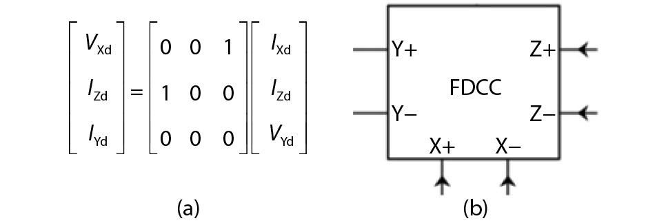
Fig. 1. (a) Matrix representation of FDCCII. (b) Symbol for FDCCII.
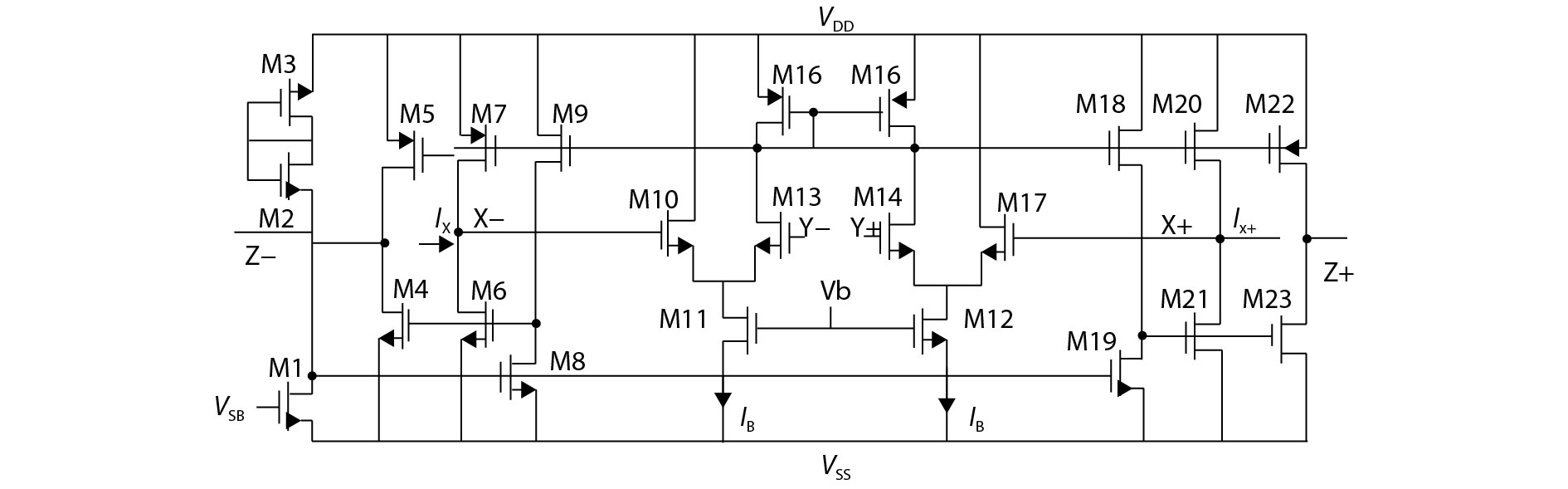
Fig. 2. CMOS FDCCII implementation.
Fig. 3. (Color online) (a) DC voltage characteristics of differential X terminal. (b) DC current response of differential Z terminal.
Fig. 4. Second order Filter realized using CMOS FDCCII (LP/BP response).
Fig. 5. LPF gain tuning (fo = 13 kHz) through R1.
Fig. 6. BPF gain tuning (fo = 13 kHz & Q = 4.08) through R1.
Fig. 7. At constant central frequency of 13 kHz, Q values varying with R2 are 3.3, 4.9 & 6.5 respectively.
Fig. 8. (a) Current division circuit (CDC). (b) Matrix representation of DCFDCCII. (c) Symbol of DCFDCCII.
Fig. 9. (Color online) DC response of Z terminals current of DCFDCCII.
Fig. 10. DCFDCCII based programmable integrator and differentiator.
Fig. 11. Observed output for codeword (a) 111111, (b) 010101.
Fig. 12. (Color online) Differentiator input & observed output for code words.
Fig. 13. (Color online) Input (inoise) and output (onoise) referred noise spectral density for (a) integrator, (b) differentiator.
VDD, VSS, VSB, Vb | 1.5, −1.5, −1.25, −0.787 V |
---|
No. of transistors | 23 | DC voltage range | −1 to 1 V | DC current range | −100 to 100 mA | −3 dB bandwidth: VZd/VYd | 82 MHz | FOM1 =(Vinmax/VDD) × 100
| 66 |
|
Table 1. Main features of FDCCII.
Transistor for FDCCII | W/L (μm/μm)
|
---|
M1, M8, M9, M18, M19 | 2/1 | M3, M5, M7, M20, M22 | 200/2 | M2, M4, M6, M21, M23 | 150/2 | M15, M16 | 100/2 | M10, M13, M14, M17 | 80/1 | M11, M12 | 80/2 | Transistor for CDN | W/L (μm/μm)
| All transistors | 1/0.35 |
|
Table 2. Aspect ratios of MOS transistors.
Characteristics | Proposed realization |
---|
Supply used | ± 1.5 V | Technology | 0.25 μm
| Fully differential | Yes | Active element | FDCCII | No. of active elements | 3 | Enjoys independent tuning | Yes | Tuning (analog/digital) | Analog | Component values | R1 = 1.3 kΩ; R2 = 2.5 kΩ (for LPF) and 10 kΩ (for BPF); R3 = 3 kΩ; R4 = 2 kΩ; C1 = 5 nF; C2 = 5 nF
|
|
Table 3. Summarized performance of proposed filter.
Reference | Adway 2000[5] | Alzaher 2003[9] | Chang 2003[6] | Shahrani 2004[13] | Mahmoud 2004[20] | Mahmoud 2005[10] | Mahmoud 2007[14] | Karac 2008[19] | This work |
---|
Technology node (μm)
| 1.2 | 1.2 | 1.2 | – | 0.35 | 0.5 | 0.35 | 0.35 | 0.25 | Active element used | FDCCII | FBCCII | FDCCII | CCII/AD844 | FDCFOA | FDCCII | FDCCII | FDCCII | FDCCII | Number of active elements used | 3 | 1 | 1 | 6 | 1 | 6 | 1 | 2 | 3 | Supply rails used (V) | ± 1.5 | ± 2.7 | ± 5 | – | ± 1.5 | ± 1.5 | ± 1.5 | ± 1.25 | ± 1.5 | Functions realized | LP BP | BP | LP BP AP BR | LP BP | LP | LP BP AP | BP | LP BP AP | LP BP | Tuning feature | N | Y | N | Y | N | Y | Y | N | Y | Fully differential | Y | Y | Y | Y | Y | Y | Y | Y | Y |
|
Table 4. Comparative study of previously reported differential second order filters.
Proposed realization | Integrator | Differentiator |
---|
Supply used | ± 1.5 V | ± 1.5 V | Technology | 0.25 μm
| 0.25 μm
| Fully differential | Yes | Yes | Active element | DCFDCCII | DCFDCCII | No. of active elements | 1 | 1 | Tuning | Digital | Digital | Component values | R = 2.5 kΩ, C = 400 pF
| C = 13 nF, R = 500 kΩ
|
|
Table 5. Summarized performance of proposed DCFDCCII applications.