
A. Tonk, N. Afzal. Second generation fully differential current conveyor based analog circuits[J]. Journal of Semiconductors, 2019, 40(4): 042401
- Journal of Semiconductors
- Vol. 40, Issue 4, 042401 (2019)
Abstract
1. Introduction
Fully differential (FD)[
The FDCCII structures that were reported in the literature employed large supply voltages, as high as 5 V[
The motivation of this treatise is to present the facility of independent analog and digital tuning of FDCCII-based analog signal processing applications related to theser two concerns. The rest of this paper is structured as follows. The first section presents a fully differential second order low-pass/band-pass filter using a six terminal CMOS FDCCII. The FDCCII is then reconfigured through digital programmability by introducing a current division circuit. Finally, a new digitally controlled FDCCII integrator and differentiator are also presented in the last section.
2. CMOS FDCCII
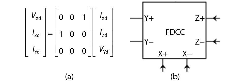
FDCCII (see the block diagram of Fig. 1(b)) has two differential X, Y and Z terminals. The fully differential buffer forces VXd to follow VYd. The FDCCII structure (see Fig. 2) has only 23 transistors unlike the available fully differential structures with 39 transistors in Refs. [9, 14]. The FD buffer consists of two matched differential pair (M10, M13) & (M 14, M17); matched biasing current source transistors (M15, M16) & (M 11, M12); and class AB output stage (M6–M9) & (M 18–M21). (M1–M3) forms the biasing of output stage and the input is applied at high impedance terminals of NMOS (M13, M14). The DC voltage characteristics of the differential X terminal and the transfer characteristics of the differential Z terminal of FDCCII are depicted by Figs. 3(a) and 3(b) respectively. Voltage and current following actions of FDCCII, as shown by the terminal equations of Fig. 1(a), exhibit nearly rail-to-rail transfer between input and output terminals. The DC current range extends from −100 to 100 mA and the DC voltage range is −1 to 1 V. The characteristic values for the FD-CCII are given in Table 1. Transistor aspect ratios are shown in Table 2.
![]()
Figure 1.(a) Matrix representation of FDCCII. (b) Symbol for FDCCII.
![]()
Figure 2.CMOS FDCCII implementation.
![]()
Figure 3.(Color online) (a) DC voltage characteristics of differential X terminal. (b) DC current response of differential Z terminal.
Table Infomation Is Not EnableTable Infomation Is Not Enable3. Proposed biquad realization and its comparison
The Sallen-Key filter,which is particularly valued for its simplicity, is a very popular active filter. It can be used to create 2nd order filter stages that can be cascaded together to form larger order filters. A Sallen-Key LP configuration has been presented in Ref. [15]
![]()
Figure 4.Second order Filter realized using CMOS FDCCII (LP/BP response).
As evident from these equations, analog tuning of the gain can be achieved by using G1, ωo by setting C1/C2 and Q by using G2. The filter gain can be expressed as: HLP = −G1/G4, HBP = −G1G2.
3.1. Sensitivity performance
The voltage gain between differential X and Y terminals, here, is not crucial because unity negative feedback has been employed in the realization. Considering the deviation of current gain involving differential X and Z terminals and taking the non-ideality into account, namely, Izdi = αiI
xdi, where i = 1, 2, 3, α = 1–ε and ε (|ε|
The sensitivities of different filter specifications are summarized below.
The proposed circuit enjoys attractive sensitivity measure. All active and passive sensitivity figures are within reasonable limits. The filter has been realized using three FDCCII blocks, using only four resistors and two capacitors. This component count is less than most of the available Sallen-Key realizations and offers the same number of output functions. It can also independently tune Q and orthogonal control of ωo & Q.
3.2. Design and verification
SPICE simulations were carried out to verify the potential of proposed second-order filter. When R1 takes values from 1.3 to 0.4 kΩ decreasing with a step size of 0.3 kΩ, gain of the LP & BP filter is found to be increasing. As R1 decreases, value of G1 increases because the two are reciprocal of each other. R1 takes values equal to {1.3, 1, 0.7, and 0.4 kΩ} for plotting low-pass and band-pass response with variable gain, as given in Figs. 5 and 6. fo has been fixed at 13 Hz and Q = 1.02 for LPF & Q = 4.08 for BPF. This variation of filter gain with resistor R1 is in agreement with the transfer functions, V01 and V02, as calculated at the beginning of Section 3. Tuning of Q-factor has been achieved by varying R2 as {8, 12, and 16 kΩ}. Here, the BP filter’s gain (see Fig. 7) can be seen to vary with R2, which again verifies the theoretical calculations. Pole-ωo tuning can be achieved by programming C1, C2 using capacitor array[
![]()
Figure 5.LPF gain tuning (
![]()
Figure 6.BPF gain tuning (
![]()
Figure 7.At constant central frequency of 13 kHz,
4. Current division circuit
Current transfer characteristics of FD-CCII block with digital control is shown in Fig. 9. Both the integrators and differentiators are prominent blocks that find applications in analog-to-digital convertors (ADCs), wave shaping circuits and continuous-time filter structures. They are considered to be very important units in the design of analog integrated and mixed-signal circuits. The output signal in an integrator is nothing but the time integral of the incoming signal. As for the differentiator, its output is directly proportional to the rate of change of the input. Earlier, most of the RC integrator and differentiator circuits were designed using operational amplifier. The major drawback of using these op-amp based circuits is that they don’t provide a spacious bandwidth and wider dynamic range. Subsequently, a few circuits have been proposed employing different current voltage-mode devices, such as OTA, CC, CCTA, etc. In this paper digitally programmable VM integrator and differentiator are shown in Fig. 10. These circuits consist of a single DCFDCCII, capacitor and resistor. They not only have the advantages of being differential but they also have versatile programmability. A routine analysis of the circuits yields the following outputs:
Fig. 8(a) shows a 6-bit M-2M ladder classical circuit which is employed at Z+ and Z- terminals of FDCCCII. Current division circuit divides input current into two branches depending on the value of a set of programmed bits. In our case, Iout1 is the ladder output that depends on the value of the α and Iout2 is grounded. N is the digital codeword. The input current is multiplied by a factor alpha, which depends on value of the first 6-bits according to:
![]()
Figure 8.(a) Current division circuit (CDC). (b) Matrix representation of DCFDCCII. (c) Symbol of DCFDCCII.
![]()
Figure 9.(Color online) DC response of Z terminals current of DCFDCCII.
![]()
Figure 10.DCFDCCII based programmable integrator and differentiator.
As evident from these equations, the time constant of the integrator and differentiator are programmable through digital code word alpha. The digital control module (CDC) is implemented for 6-bit. The circuits are simulated with SPICE tool of the TSMC 0.25 μm CMOS process. A pulse input of −0.5 to + 0.5 V and 10 μs time period is applied (high for 5 μs and low for 5 μs). The VM integrator circuit is designed for R = 2.5 kΩ, C = 400 pF. The observed wave shapes for different control word alpha are shown in Fig. 11. The VM differentiator circuit is designed for R = 500 kΩ and C = 13 nF. An input with magnitude 0.5 V is applied and wave shapes observed for different control word alpha are shown in Fig. 12.
![]()
Figure 11.Observed output for codeword (a) 111111, (b) 010101.
![]()
Figure 12.(Color online) Differentiator input & observed output for code words.
The input and output noise spectral densities for CMOS FDCCII based reconfigurable integrator and differentiator are presented in Figs. 13(a) and 13(b). This verifies the essential input to output noise-suppression capability of a differential building block. All of the results that we obtained confirm the theory. The performance of the two realizations is summarized in Table 5.
![]()
Figure 13.(Color online) Input (inoise) and output (onoise) referred noise spectral density for (a) integrator, (b) differentiator.
5. Conclusion
A second order LP/BP filter and reconfigurable integrator and differentiator have been realized using CMOS based FDCCII and its digital variant DCFDCCII respectively. The filter has independent analog tuning of gain, ωo and Q. The integrator's and differentiator's response are digitally controlled. Our simulation results are based on 0.25 μm technology and 1.5 V supply voltage. This is our dedicated effort to present the facility of analog and digital tuning of FDCCII block.
Acknowledgment
The authors would like to thank Department of Electronics, Jamia Millia Islamia University and UGC for providing valuable support in form of the NET-JRF grant.
References
[1] J Mohan, B Chaturvedi, S. Maheshwari. Low voltage mixed mode multi phase oscillator using single FDCCII. Electronics, 20, 36(2016).
[2] F Kaçar, A Yeşil. FDCCII-based FDNR simulator topologies. Int J Electron, 99, 285(2012).
[3] S Maheshwari, P Beg, I A Khan et al. Digitally programmable fully differential filter. Radioengineering, 20, 917(2011).
[4] F Gür, F Anday. Simulation of a novel current mode universal filter using FDCCIIs. Analog Integr Circuits Signal Process, 60, 231(2009).
[5] A A El-Adawy, A M Soliman, H O Elwan. A novel fully differential current conveyor and applications for analog VLSI. IEEE Trans Circuits Syst II, 47, 306(2000).
[6] C M Chang, B M Al-Hashimi, C L Wang et al. Single fully differential current conveyor biquad filters. IEEE Proceedings-Circuits Devices and Systems, 150, 394(2003).
[7]
[8]
[9] H A Alzaher, H Elwan, M Ismail. A CMOS fully balanced second-generation current conveyor. IEEE Trans Circuits Syst II, 50, 278(2003).
[10] S A Mahmoud, M A Hashiesh, A M Soliman. Low-voltage digitally controlled fully differential current conveyor. IEEE Trans Circuits Syst I, 52, 2055(2005).
[11]
[12] J W Horng. Fully differential first-order all pass filters using a DDCC. Ind J Eng Mater Sci, 21, 345(2014).
[13]
[14] S A Mahmoud. Fully differential CMOS CCII based on differential difference transconductor. Analog Integrated Circuits and Signal Processing, 50, 195(2007).
[15] B Chipipop, W Surakampontorn. Realisation of current-mode FTFN-based inverse filter. Electron Lett, 35, 690(1999).
[16] C H Wu, H H Hsieh, P C Ku et al. A differential Sallen-key low-pass filter in amorphous-silicon technology. J Display Technol, 6, 207(2010).
[17] V Stornelli, G Ferri. A 0.18
[18] S Minaei, M A Ibrahim. General configuration for realizing current-mode first-order all-pass filter using DVCC. Int J Electron, 92, 347(2005).
[19] F Kacar, H Kuntman, S Özcan. New high performance CMOS fully differential current conveyor. Electrosocope(2008).
[20] S A Mahmoud. Low voltage fully differential CMOS current feedback operational amplifier. The 47th IEEE Midwest Symposium on Circuits and Systems, 1, I-49(2004).

Set citation alerts for the article
Please enter your email address
© Copyright 2018-2021 | Chinese Laser Press. All Rights Reserved 沪ICP备15018463号-20