
Quan Wang, Changxi Chen, Wei Li, Yanbin Qin, Lijuan Jiang, Chun Feng, Qian Wang, Hongling Xiao, Xiufang Chen, Fengqi Liu, Xiaoliang Wang, Xiangang Xu, Zhanguo Wang. Fabrication and characterization of AlGaN/GaN HEMTs with high power gain and efficiency at 8 GHz[J]. Journal of Semiconductors, 2021, 42(12): 122802
- Journal of Semiconductors
- Vol. 42, Issue 12, 122802 (2021)
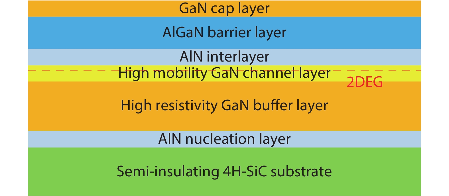
Fig. 1. (Color online) The schematic of the grown AlGaN/GaN HEMT structure.
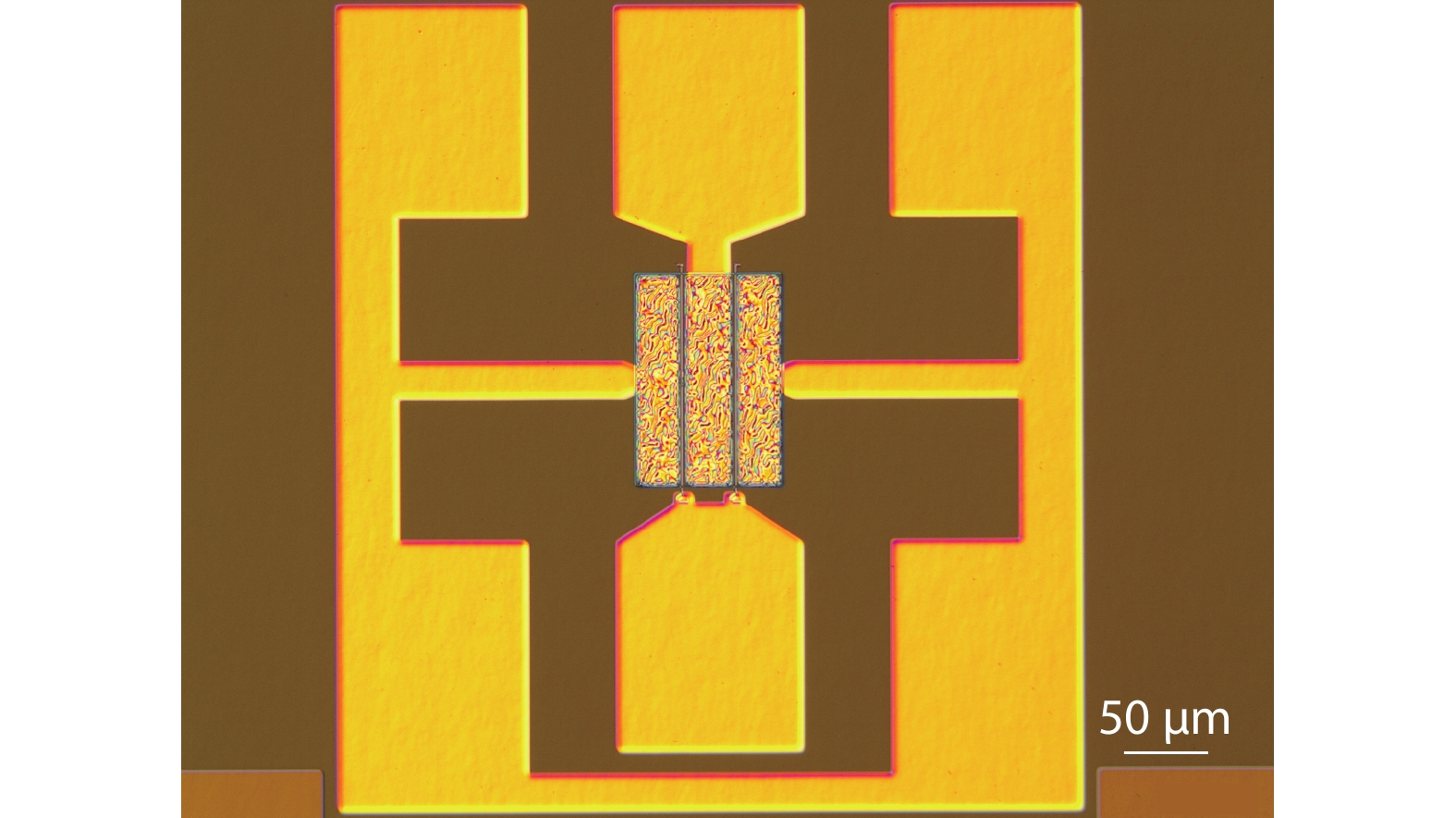
Fig. 2. (Color online) The microscope photograph of the fabricated double-finger GaN HEMT with a L G of 0.45 µ m and total W G of 200 µ m. The pad is designed to be suitable for ground-signal-ground (GSG) probe.
Fig. 3. (Color online) The HRXRD results of the AlGaN/GaN HEMT structure with (a) ω -scan of (0002) and (b) (10-12) diffraction peaks, and (c) ω –2θ scan of (0004) planes.
Fig. 4. (Color online) The results of Non-contact Hall measurements at room temperature with average values of 2DEG (a) mobility and (b) concentration being 2291.1 cm2/(V·s) and 9.954 × 1012 cm–2, respectively.
Fig. 5. (Color online) Typical output characteristic (a) I DS–V DS and transfer characteristics (b) I DS–V GS. In PIV mode, each pulse cycle includes an on-state pulse of 300 µ s with a duty cycle of 0.3%.
Fig. 6. (Color online) The extrinsic small signal characteristics of the fabricated AlGaN/GaN HEMT device.
Fig. 7. (Color online) The power performances of the fabricated AlGaN/GaN HEMT device. The measurement was performed under PW-mode with a pulse width of 100 μ s and a duty cycle of 1%. The bias was in class-AB operation, under (a) (–3.5, 28) V, (b) (–3.5, 34) V and (c) (–3.5, 40) V gate/drain direct current (DC) bias, respectively.
Fig. 8. (Color online) The obtained P out, PAE and power gain, depicted as a function of V DS. During the measurement, the P in was fixed in 18 dBm, and the V GS was fixed in –3.5 V.
Fig. 9. (Color online) Pulsed current-voltage characteristics of the device. Measurements are taken under different quiescent bias point (V GSQ, V DSQ), as indicated in the graph. Each test pulse period consists of a 1 μ s on-state pulse, followed by a 999 μ s off-state pulse (0.1% duty cycle). Here V GS is taken from –6.0 to 2.0 V in steps of 1.0 V.
|
Table 1. The growth parameters of the AlGaN / GaN HEMT structure.
|
Table 2. The detailed measurement results of power performances of the fabricated AlGaN/GaN HEMT device.
|
Table 3. The calculated possible output power and drain efficiency corresponding to different V DS from 28 to 40 V when V GS = –3.5 V.

Set citation alerts for the article
Please enter your email address
© Copyright 2018-2021 | Chinese Laser Press. All Rights Reserved 沪ICP备15018463号-20