• Journal of Semiconductors
  • Vol. 42, Issue 12, 122802 (2021)
Quan Wang1、2、3, Changxi Chen3、4, Wei Li3、4, Yanbin Qin3、4, Lijuan Jiang3、4、5, Chun Feng3、4、5, Qian Wang3、5, Hongling Xiao3、4、5, Xiufang Chen1、2, Fengqi Liu3、4、5, Xiaoliang Wang3、4、5, Xiangang Xu1、2, and Zhanguo Wang3、4
Author Affiliations
  • 1State Key Laboratory of Crystal Materials, Shandong University, Jinan 250100, China
  • 2Institute of Novel Semiconductors, Shandong University, Jinan 250100, China
  • 3Key Lab of Semiconductor Materials Science, Institute of Semiconductors, Chinese Academy of Sciences, Beijing 100083, China
  • 4Center of Materials Science and Optoelectronics Engineering and School of Microelectronics, University of Chinese Academy of Sciences, Beijing 100049, China
  • 5Beijing Key Laboratory of Low Dimensional Semiconductor Materials and Devices, Beijing 100083, China
  • show less
    DOI: 10.1088/1674-4926/42/12/122802 Cite this Article
    Quan Wang, Changxi Chen, Wei Li, Yanbin Qin, Lijuan Jiang, Chun Feng, Qian Wang, Hongling Xiao, Xiufang Chen, Fengqi Liu, Xiaoliang Wang, Xiangang Xu, Zhanguo Wang. Fabrication and characterization of AlGaN/GaN HEMTs with high power gain and efficiency at 8 GHz[J]. Journal of Semiconductors, 2021, 42(12): 122802 Copy Citation Text show less

    Abstract

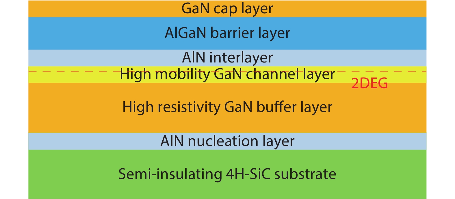
    State-of-the-art AlGaN/GaN high electron mobility structures were grown on semi-insulating 4H-SiC substrates by MOCVD and X-band microwave power high electron mobility transistors were fabricated and characterized. Hall mobility of 2291.1 cm2/(V·s) and two-dimensional electron gas density of 9.954 × 1012 cm–2 were achieved at 300 K. The HEMT devices with a 0.45-μm gate length exhibited maximum drain current density as high as 1039.6 mA/mm and peak extrinsic transconductance of 229.7 mS/mm. The fT of 30.89 GHz and fmax of 38.71 GHz were measured on the device. Load-pull measurements were performed and analyzed under (–3.5, 28) V, (–3.5, 34) V and (–3.5, 40) V gate/drain direct current bias in class-AB, respectively. The uncooled device showed high linear power gain of 17.04 dB and high power-added efficiency of 50.56% at 8 GHz when drain biased at (–3.5, 28) V. In addition, when drain biased at (–3.5, 40) V, the device exhibited a saturation output power density up to 6.21 W/mm at 8 GHz, with a power gain of 11.94 dB and a power-added efficiency of 39.56%. Furthermore, the low fmax/fT ratio and the variation of the power sweep of the device at 8 GHz with drain bias voltage were analyzed.
    $ {f_{\rm T}} = \frac{1}{{2\pi \tau }} = \frac{1}{{2\pi \left( {\dfrac{{{L_{\rm G}}}}{{{v_{\rm{ch}}}}} + \dfrac{{{L_{\rm{GDd}}}}}{{2{v_{\rm{d}}}}}} \right)}}, $ (1)

    View in Article

    $ {f_{\rm{max} }} = \dfrac{{{f_{\rm{T}}}}}{{2{{\left( { {\dfrac{{{R_{\rm{G}}} + {R_{\rm{GS}}} + {R_{\rm{S}}}}}{{{R_{\rm{DS}}}}}} + 2\pi {f_{\rm{T}}}{C_{\rm{GD}}}{R_{\rm{G}}}} \right)}^{\frac{1}{2}}}}}, $ (2)

    View in Article

    $ {I_{\rm{DC}}} = \frac{{{I_{{\rm{Dmax}} }}}}{{2\pi }} \cdot \frac{{2 \, \sin (\alpha /2) - \alpha \, \cos (\alpha /2)}}{{1 - \cos (\alpha /2)}}, $ (3)

    View in Article

    $ {I_1} = \frac{{{I_{{\rm{Dmax}} }}}}{{2\pi }} \cdot \frac{{\alpha - \sin \alpha }}{{1 - \cos (\alpha /2)}}, $ (4)

    View in Article

    $ {P_{\rm{out}}} = \frac{1}{8}\left( {\Delta I \cdot \Delta V} \right), $ (5)

    View in Article

    $\begin{array}{l} \rm{PAE} = {\eta _{\rm{D}}} \cdot \dfrac{1}{{1 + {V_{\rm{K}}}/{V_{\rm{DC}}}}} \cdot \dfrac{1}{{1 + {I_{{\rm{min}}}}/{I_{\rm{DC}}}}} \cdot \dfrac{1}{{1 + \Delta {I_{\rm{DC-RF}}}/{I_{\rm{DC}}}}} \\ \quad\qquad\times\left( {1 - {\omega ^2}C_{\rm{GD}}^2 + {R_{\rm{GD}}}{R_{\rm{L}}}} \right)\left( {1 - \dfrac{1}{G}} \right), \end{array}$ (6)

    View in Article

    Quan Wang, Changxi Chen, Wei Li, Yanbin Qin, Lijuan Jiang, Chun Feng, Qian Wang, Hongling Xiao, Xiufang Chen, Fengqi Liu, Xiaoliang Wang, Xiangang Xu, Zhanguo Wang. Fabrication and characterization of AlGaN/GaN HEMTs with high power gain and efficiency at 8 GHz[J]. Journal of Semiconductors, 2021, 42(12): 122802
    Download Citation