
Quan Wang, Changxi Chen, Wei Li, Yanbin Qin, Lijuan Jiang, Chun Feng, Qian Wang, Hongling Xiao, Xiufang Chen, Fengqi Liu, Xiaoliang Wang, Xiangang Xu, Zhanguo Wang. Fabrication and characterization of AlGaN/GaN HEMTs with high power gain and efficiency at 8 GHz[J]. Journal of Semiconductors, 2021, 42(12): 122802
- Journal of Semiconductors
- Vol. 42, Issue 12, 122802 (2021)
Abstract
1. Introduction
Since the first realization of AlGaN/GaN high electron mobility transistors (HEMTs)[
X-band power amplifiers are used in military and commercial radar systems, as well as communication data links; indeed, these applications demand high power gain (G), high power efficiency and suitable power specifications. GaN HEMTs have been proved to be an ideal candidate with high power densities[
In this paper, AlGaN/GaN HEMT structural materials with high mobility, high two-dimensional electron gas density and high uniformity were grown using a metal-organic chemical vapor deposition (MOCVD) system. HEMT devices were fabricated and their small and large signal properties were characterized. HEMT devices operating at 8 GHz with high power gain and high power-added efficiency (PAE) were realized although trapping effects were not removed completely.
2. HEMT structure growth and device fabrication
2.1. HEMT structure growth
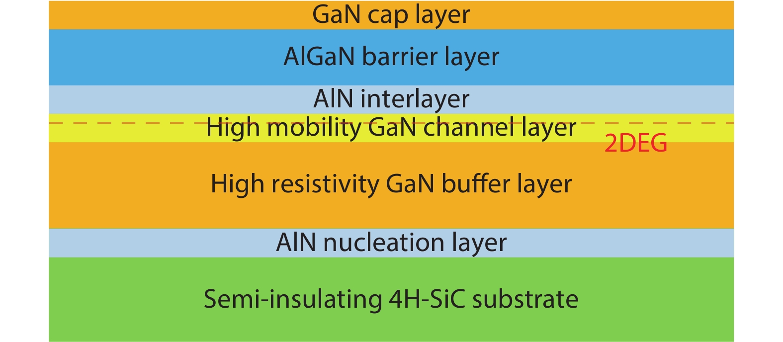
The schematic of the AlGaN/GaN HEMT structure used in this study is shown in Fig. 1, which was grown by MOCVD on 4-inch SI 4H-SiC substrate. AlN nucleation layer, GaN buffer layer with high resistivity, GaN layer with high mobility, AlN interlayer, AlGaN barrier layer and GaN cap layer were grown in sequence. The specific growth parameters are shown in Table 1.
![]()
Figure 1.(Color online) The schematic of the grown AlGaN/GaN HEMT structure.
Table Infomation Is Not EnableThe introduction of the GaN channel layer with high crystal quality can enhance the mobility of 2DEG. Compared with the conventional AlGaN/GaN heterostructures, the insertion of the AlN interlayer can provide higher barrier, which improve the discontinuity of the conduction band and the confinement of the electron wave function[
High-resolution X-ray diffraction (HRXRD, by PANalytical X'Pert3 MRD) was adopted to study the crystalline quality and structural properties, while electrical properties were obtained by the room temperature (300 K) non-contact Hall measurements (by Semilab LEI 1610E 100AM). Non-contact sheet resistance measurements (by Semilab LEI 1510C) were carried out at 300 K to characterize the square resistance and their uniformity of the epi-wafers.
2.2. Device fabrication
The fabrication of devices begins with the formation of drain and source ohmic contacts. The selected metals for ohmic contacts are composed of Ti (20 nm)/Al (120 nm)/Ni (55 nm)/Au (50 nm), deposited by electron beam evaporation, and followed by rapid thermal annealing (RTA) at 850 °C for 30 s in N2 ambient. The specific ohmic contact resistance of 1.67 × 10⁻⁶ Ω·cm2 was measured by the transmission line method (TLM). Mesa isolation was conducted by inductively coupled plasma (ICP) dry etching. Afterwards, Si3N4 was deposited by plasma enhanced chemical vapor deposition (PECVD) as the passivation layer. By reactive ion etching (RIE), a 0.45-μm gate recess was formed, then the Schottky T-gate composed of Ni/Au was evaporated and lifted off. Finally, a silicon nitride film was deposited using PECVD to passivate the devices. The measured double-finger device has a gate length (LG) of 0.45 µm and total gate width (WG) of 200 µm, a source-to-gate distance (LSG) of 1.1 µm, and a source-to-drain distance (LSD) of 4.5 µm. A microscope photograph of the fabricated GaN HEMT is shown in Fig. 2. In order to facilitate on-chip testing, the pad is designed to be suitable for a ground-signal-ground (GSG) probe.
![]()
Figure 2.(Color online) The microscope photograph of the fabricated double-finger GaN HEMT with a
The direct current (DC) and pulsed output I–V characteristics of the double-finger device were carried out using an Agilent B2902A dual-channel precision source/measure unit (SMU). The extrinsic small-signal characteristics of the devices was measured by on-wafer probing from 0.1 to 35 GHz using a SUSS |Z| probe and Agilent E8363B vector network analyzer. The Focus load-pull system were used to carried out the AlGaN/GaN HEMT device source-pull and load-pull measurements in pulse wave (PW) mode with a pulse width of 100 μs and a duty cycle of 1% at the frequency of 8 GHz without intentional harmonic matching. For all the measurements above, the devices were not cooled and the measurements were carried at 300 K.
3. Results and discussion
Shown in Fig. 3 is the HRXRD measured results of the MOCVD-grown AlGaN/GaN HEMT structure. The full widths at half maximum (FWHM) of the (0002) and (10-12) peaks are presented in Figs. 3(a) and 3(b), with values of 266 and 324 arc seconds, respectively. Screw-type dislocation densities (STDDs) and edge-type dislocation densities (ETDDs) can be calculated using the FWHM as 1.422 × 10⁸ and 8.768 × 108 cm–3, respectively[
![]()
Figure 3.(Color online) The HRXRD results of the AlGaN/GaN HEMT structure with (a)
The results of non-contact Hall measurements are given in Fig. 4. Mapping results in Figs. 4(a) and 4(b) show that the average value of 2DEG mobility is as high as 2291.1 cm2/(V·s) and 2DEG concentration is 9.954 × 1012 cm–2, respectively. Furthermore, the epi-wafer exhibited an average sheet resistance (Rsh) of 301.6 Ω/square with a uniformity of 1.64%. All these measured results indicate that our MOCVD-grown AlGaN/GaN HEMT structures are among the state-of-the-art in literature, having excellent properties and being suitable for the fabrication of high-performance devices.
![]()
Figure 4.(Color online) The results of Non-contact Hall measurements at room temperature with average values of 2DEG (a) mobility and (b) concentration being 2291.1 cm2/(V·s) and 9.954 × 1012 cm–2, respectively.
Since the processed AlGaN/GaN HEMT devices were on a 330-μm thick SI-SiC substrate without thinning, to evaluate and decrease the self-heating effect[
![]()
Figure 5.(Color online) Typical output characteristic (a)
The kink effect[
Small signal microwave performance was characterized. Measured current-gain H21 and maximum available power-gain (MAG) as a function of frequency are shown in Fig. 6. The unit current gain cut-off frequency (fT) and the maximum frequency of oscillation (fmax) was obtained from the extrapolation of H21 and MAG to unity using a –6 dB/octave slope. When the source–drain bias voltage was fixed at 15 V and the source–gate bias voltage at –3.0 V, the measured fT and fmax is 30.89 and 38.71 GHz, respectively.
![]()
Figure 6.(Color online) The extrinsic small signal characteristics of the fabricated AlGaN/GaN HEMT device.
Physically, for a FET, fT is the inverse of the total transit time τ[
where LG is the gate length, vch is the effective electron velocity in the channel, LGDd is the gate–drain depletion length and vd is the electron velocity in the depletion region. While the extrinsic small-signal characteristics of the AlGaN/GaN device was measured, the source–drain bias voltage was fixed at 15 V larger than the knee voltage 4.2 V. Due to either velocity saturation or pinch-off under the drain side of the channel, fT approaches its peak. The gate length of the device is 0.45 μm. Supposing that the drain extension is zero and that the electron velocity arrives at the high field saturation velocity of 1.5 × 107 cm/s by Monte Carlo simulation[
Fig. 6 shows that the fmax/fT ratio is 1.253. fmax has the following dependence on parasitics[
where RG is the gate resistance, RS is source resistance, CGD is gate–drain capacitance, CGS is gate–source capacitance and RGS is the channel resistance in series with CGS. Generally, CGD is very small, which can be ignored. The low fmax/fT ratio is related to the access resistance, the relatively low resistance of the semi-insulating GaN buffer, and output conductance. For our devices, because the T-gate cap is 150 nm thick much smaller than 1.0 μm, large RG is one of the possible reasons responsible for the low fmax/fT ratio. By shortening the gate length, gate-recessing, and reducing parasitics, fT and fmax/fT ratio can be increased.
Large signal microwave measurements were performed on the wafer without cooling. Fig. 7 shows load-pull results of a 2 × 100 × 0.45 µm AlGaN/GaN HEMT device measured in PW-mode with a pulse width of 100 μs and a duty cycle of 1% by the Focus load-pull system at the frequency of 8 GHz without intentional harmonic matching. The bias was in class-AB operation, under (–3.5, 28) V, (–3.5, 34) V and (–3.5, 40) V gate/drain direct current (DC) bias, respectively. The detailed measurement results are shown in Table 2.
![]()
Figure 7.(Color online) The power performances of the fabricated AlGaN/GaN HEMT device. The measurement was performed under PW-mode with a pulse width of 100
Fig. 7(a) shows the power sweep at a drain bias of 28 V with a linear gain of 17.04 dB. A maximum Pout of 30.54 dBm achieved at Pin = 19.54 dBm with an associated power gain of 11.00 dB and PAE of 50.56%., the gain compression being 6 dB. The saturated output power density is 5.66 W/mm.
Fig. 7(b) gives the power sweep at a drain bias of 34 V with a linear gain of 18.22 dB. A maximum Pout of 30.61 dBm achieved at Pin = 18.52 dBm with an associated power gain of 12.09 dB and PAE of 46.67%, the gain compression being 6 dB. The saturated output power density is 5.75 W/mm.
Fig. 7(c) indicates the power sweep at a drain bias of 40 V with a linear gain of 18.19 dB. A maximum Pout of 30.94 dBm achieved at Pin = 19.00 dBm with an associated power gain of 11.94 dB and PAE of 39.56%, the gain compression being 6 dB. The saturated output power density is 6.21 W/mm.
In Fig. 8, the obtained Pout, power gain, PAE and drain efficiency, are depicted as a function of VDS, during the measurement, the Pin was fixed to 18 dBm, and the VGS was fixed in –3.5 V. The output power and power gain increase with increasing VDS, from 30.15 to 30.71 dBm, and 12.15 to 12.70 dB, respectively. The PAE and drain efficiency decrease with increasing VDS from 50.43% to 39.94%, and 54.35% to 42.21%, respectively.
![]()
Figure 8.(Color online) The obtained
For an ideal HEMT in class-AB operation, the DC and the corresponding fundamental current components of the output current waveform can be calculated by Fourier analysis according to[
where α is the conduction angle.
The maximum output power can be calculated according to the following formula:
where ∆I = 2I1 and ∆V = 2(VDS − VK) are the RF current swing and voltage swing. This predicts a possible output power density provided that an ultimate thermal management is properly done. For the devices fabricated by us, the VK extracted from the DC output characteristics is 4.2 V, and the IDmax was obtained to be 1039.60 mA/mm at a gate bias of 2.0 V. The conduction angle was calculated to be 105.83°. From the formulas above it is easy to know the possible output power and maximum drain efficiency (ηD) corresponding to different VDS from 28 to 40 V. The calculated results are given in Table 3, showing that with increasing the VDS, both the DC power supply and the output fundamental power as well as the maximum ηD will increase.
The ηD almost keeps constant at about 62.8% with a slightly increase when VDS increases from 28 to 40 V. If the VK = 0 V, the calculated maximum ηD will be 71.87% being constant for all VDS. The calculated maximum output power is 6.53, 8.17 and 9.82 W/mm, respectively, when VDS are 28, 34 and 40 V. However, our measured output power at the corresponding VDS are 5.66, 5.71 and 6.21 W/mm, respectively, as shown in Fig. 7 and Table 2. It is evident that the higher the VDS, the more difference between the ideal maximum output power and the measured output power at a power gain compression of 6 dB. The most evident is that the measured maximum ηD is much lower than the calculated counterpart and they decrease faster and faster with increasing the VDS, implying that the decrease of the measured ηD is correlated to the increase of the VDS, which therefore make the output power at VDS = 40 V nearly the same as that of VDS = 28 V.
The above calculation is based on an important condition that both the RF current swing ∆I and the VK are constants while changing the VDS. When this condition is not satisfied, the change of the ideal maximum output power density with VDS will not be linear.
One of the main limiting factors to high performance in GaN HEMTs is the current collapse or DC-to-RF dispersion caused by trapping effects[
![]()
Figure 9.(Color online) Pulsed current-voltage characteristics of the device. Measurements are taken under different quiescent bias point (
Fig. 9 shows there exist trapping effects in our devices and gives an idea of the amount of trapping in the structure. The Ron increase is obvious in large VDS stress and inconspicuous in large VGS bias, and the output current IDS also decrease under the influence of stress. As a result, large VDS stress leads to an increase in VK and decrease in IDS. Moreover, with further increase of VDS stress, the current collapse will become more serious[
The power and efficiency performance of an AlGaN/GaN HEMT is mainly limited due to the following factors: (a) Knee voltage VK; (b) Drain leakage current Imin; (c) Current collapse or DC-to-RF dispersion ΔIDC-RF; (d) Feedback; (e) Compression behavior; (f) Thermal effects and reliability. Taking all these factors from (a) to (e) into consideration, the realizable power-added efficiency amounts can be estimated by[
PAE is mainly determined by the VK and ΔIDC-RF/IDC. The VK has a deep impact on the PAE behavior of a transistor due to the fact that it will always be a significant percentage of the DC supply[
4. Conclusion
We have grown state-of-the-art AlGaN/GaN HEMT structure materials on 4-inch SI 4H-SiC substrates and fabricated X-band HEMT microwave power devices of 0.45-μm gate length with high linear power gain of 17.04 dB and high power-added-efficiency of 50.56% at 8 GHz when drain biased at 28 V in class-AB operation. The 2DEG mobility and concentration of the HEMT structure were measured to be 2291.1 cm2/(V·s) and 9.954 × 1012 cm–2, respectively. A low average Rsh of 301.6 Ω/square with uniformity of 1.64% is achieved. For the fabricated HEMT devices, DC and PIV drain saturation current density are 1039.60 and 1086.35 mA/mm, and the peak extrinsic transconductances are obtained to be 226.70 and 229.70 mS/mm at a gate bias of –3.0 V, respectively. The fT and fmax of the device were measured to be 30.89 and 38.71 GHz, respectively. Large RG is one of the possible reasons responsible for the low fmax/fT ratio of 1.253. When device drain was biased at 28, 34 and 40 V and gate at –3.5 V in class-AB, our measured output power density of the device without cooling is 5.66, 5.71 and 6.21 W/mm, with power gains and PAEs of 11.00 dB and 50.56%, 12.09 dB and 46.67%, and 11.94 dB and 39.56%, respectively. The measured output power densities are lower than the ideally expected maximum output power of 6.53, 8.17 and 9.82 W/mm at corresponding drain–source biases, due to the effects of possibly existing traps in the HEMTs on RF knee voltage and maximum output current with increasing drain–source bias. Although the DC-to-RF dispersion still exists in our devices, by using the state-of-the-art HEMT structural materials, surface passivation technology and field plate, HEMTs with high gain and high efficiency were achieved.
Acknowledgements
We would like to thank Prof. Xiaodong Wang for providing the experimental conditions, and Dr. Wei Yan and Mr. Desong Wang for their help in EBL and optical lithography. This work was supported by the National Key Research and Development Program of China (2017YFB0402900), the Key-Area Research and Development Program of Guangdong Province (2019B010126001), the Natural Science Foundation for Distinguished Young Scholars of Shandong Province (ZR2019JQ01), the National Natural Sciences Foundation of China (62074144, 52022052, 62004118), Key R & D plan of Shandong Province (2019JMRH0901, 2019JMRH0201), the Natural Science Foundation of Shandong Province (ZR2019BEM030, ZR2019BEM011).
References
[1] M A Khan, J N Kuznia, A R Bhattarai et al. Metal semiconductor field effect transistor based on single crystal GaN. Appl Phys Lett, 62, 1786(1993).
[2] O Ambacher, rt J Smart, y J R Shealy et al. Two-dimensional electron gases induced by spontaneous and piezoelectric polarization in undoped. J Appl Phys, 85, 3222(2000).
[3] S C Jain, M Willander, J Narayan et al. III-nitrides: Growth, characterization, and properties. J Appl Phys, 87, 965(2000).
[4] X L Wang, G X Hu, Z Y Ma et al. MOCVD-grown AlGaN/AlN/GaN HEMT structure with high mobility GaN thin layer as channel on SiC. Chin J Semicond, 27, 1521(2006).
[5] A Fletcher, D Nirmal, J Ajayan et al. An intensive study on assorted substrates suitable for high JFOM AlGaN/GaN HEMT. Silicon, 13, 1591(2020).
[6] Y Gao, H Zhang, Y Zong et al. 150 mm 4H-SiC substrate with low defect density. Mater Sci Forum, 858, 41(2016).
[7] B K Jang, J H Park, J W Choi et al. Modified hot-zone design of growth cell for reducing the warpage of 6"-SiC wafer. Mater Sci Forum, 1004, 32(2020).
[8] U K Mishra, P Parikh, Y F Wu. AlGaN/GaN HEMTs-an overview of device operation and applications. Proc IEEE, 90, 1022(2002).
[9] R S Pengelly. A review of GaN on SiC high electron-mobility power transistors and MMICs. IEEE Trans Microwave Theory Tech, 60, 1764(2012).
[10] V Camarchia, R Quaglia, A Piacibello et al. A review of technologies and design techniques of millimeter-wave power amplifiers. IEEE Trans Microwave Theory Tech, 68, 2957(2020).
[11] X L Wang, T S Chen, H L Xiao et al. High-performance 2 mm gate width GaN HEMTs on 6H-SiC with output power of 22.4W@8GHz. Solid-State Electron, 52, 926(2008).
[12] X L Wang, T S Chen, H L Xiao et al. An internally-matched GaN HEMTs device with 45.2 W at 8 GHz for X-band application. Solid State Electron, 53, 332(2009).
[13] Q Wang, X L Wang, H L Xiao et al. X-band GaN high electron mobility transistor power amplifier on 6H-SiC with 110 W output power. J Nanosci Nanotechnol, 18, 7451(2018).
[14] U K Mishra, L Shen, T E Kazior et al. GaN-based RF power devices and amplifiers. Proc IEEE, 96, 287(2008).
[15] C Chen, R Sadler, D Wang et al. The interplay of thermal, time and Poole-Frenkel emission on the trap-based physical modeling of GaN HEMT drain characteristics. 2017 IEEE Compound Semiconductor Integrated Circuit Symposium (CSICS), 1(2017).
[16] K Kellogg, S Khandelwal, L Dunleavy et al. Characterization of thermal and trapping time constants in a GaN HEMT. 2020 94th ARFTG Microwave Measurement Symposium (ARFTG), 1(2020).
[17] L Q Zhang, P F Wang. AlGaN/GaN HEMT with LPCVD deposited SiN and PECVD deposited SiCOH low-k passivation. Appl Phys Express, 12, 036501(2019).
[18] A Nakajima, K Itagaki, K Horio. Effects of field plate on buffer trapping in AlGaN/GaN HEMTs. Phys Status Solidi C, 6, 2840(2009).
[19] Y Bi, X L Wang, H L Xiao et al. The influence of the InGaN back-barrier on the properties of Al0.3Ga0.7N/AlN/GaN/InGaN/GaN structure. Eur Phys J-Appl Phys, 55, 10102(2011).
[20] L Shen, S Heikman, B Moran et al. AlGaN/AlN/GaN high-power microwave HEMT. IEEE Electron Device Lett, 22, 457(2001).
[21] E T Yu, X Z Dang, L S Yu et al. Schottky barrier engineering in III-V nitrides via the piezoelectric effect. Appl Phys Lett, 73, 1880(1998).
[22] T Gessmann, J W Graff, Y L Li et al. Ohmic contact technology in III-V nitrides using polarization effects in cap layers. IEEE Lester Eastman Conference on High Performance Devices, 492(2002).
[23] S Arulkumaran, T Egawa, H Ishikawa. Studies on the influences of i-GaN, n-GaN, p-GaN and InGaN cap layers in AlGaN/GaN high-electron-mobility transistors. Jpn J Appl Phys, 44, 2953(2005).
[24] J M Gong, Q Wang, J D Yan et al. Comparison of GaN/AlGaN/AlN/GaN HEMTs grown on sapphire with Fe-modulation-doped and unintentionally doped GaN buffer: Material growth and device fabrication. Chin Phys Lett, 33, 103(2016).
[25] M Singh, M J Uren, T Martin et al. 'Kink' in AlGaN/GaN-HEMTs: Floating buffer model. IEEE Trans Electron Devices, 65, 3746(2018).
[26] L H Fu, H Lu, D J Chen et al. Field-dependent carrier trapping induced kink effect in AlGaN/GaN high electron mobility transistors. Appl Phys Lett, 98, 586(2011).
[27] M A Alim, S Afrin, A A Rezazadeh et al. Thermal response and correlation between mobility and kink effect in GaN HEMTs. Microelectron Eng, 219, 111148.1(2020).
[28]
[29] B Gelmont, K Kim, M Shur. Monte Carlo simulation of electron transport in gallium nitride. J Appl Phys, 74, 1818(1993).
[30]
[31]
[32] A M Darwish, B D Huebschman, E Viveiros et al. Dependence of GaN HEMT millimeter-wave performance on temperature. IEEE Trans Microwave Theory Tech, 57, 3205(2009).
[33] J Kühn. AlGaN/GaN-HEMT power amplifiers with optimized power-added efficiency for X-band applications. KIT Scientific Publishing(2011).
[34] R Vetury, N Q Zhang, S Keller et al. The impact of surface states on the DC and RF characteristics of AlGaN/GaN HFETs. IEEE Trans Electron Devices, 48, 560(2001).
[35] R Chu, L Shen, N Fichtenbaum et al. Correlation between DC–RF dispersion and gate leakage in deeply recessed GaN/AlGaN/GaN HEMTs. IEEE Electron Device Lett, 29, 303(2008).

Set citation alerts for the article
Please enter your email address
© Copyright 2018-2021 | Chinese Laser Press. All Rights Reserved 沪ICP备15018463号-20