• Journal of Semiconductors
  • Vol. 43, Issue 4, 041106 (2022)
Xiaomei Wu, Xiaoxing Ke, and Manling Sui
Author Affiliations
  • Faculty of Materials and Manufacturing, Beijing University of Technology, Beijing 100124, China
  • show less
    DOI: 10.1088/1674-4926/43/4/041106 Cite this Article
    Xiaomei Wu, Xiaoxing Ke, Manling Sui. Recent progress on advanced transmission electron microscopy characterization for halide perovskite semiconductors[J]. Journal of Semiconductors, 2022, 43(4): 041106 Copy Citation Text show less
    (Color online) Schematic illustration of advanced TEM characterization for halide perovskites.
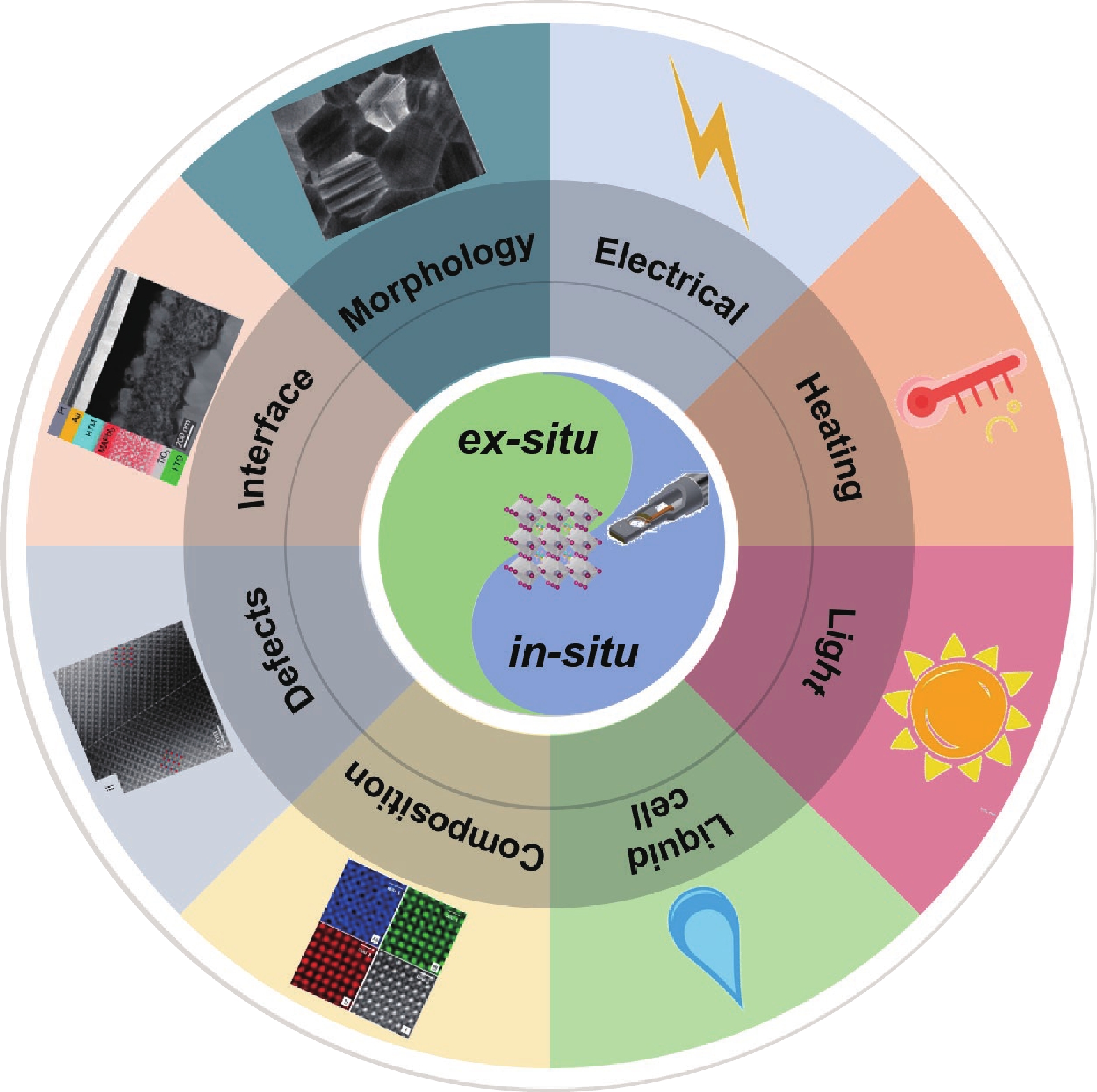
    Fig. 1. (Color online) Schematic illustration of advanced TEM characterization for halide perovskites.
    (Color online) (a) Electron beam irradiation damage observed in free-standing MAPbI3 films. (i, ii). TEM images recorded initially and after the irradiation (9870 e/(Å2·s) for ~2 min), respectively[47]. (b) Time-series of TEM images on MAPbI3 single crystal showing the electron beam damage from 0 to 50 s, where bubble-like morphology (colored arrows) emerged and grew[49]. (c) Time-series of TEM images obtained on BA2PbBr4 nanosheets[53]. (d) TEM images of the (i) CsPbCl3, (ii) CsPbBr3 and (iii) CsPbI3QDs where "dark spots" present at the QD corners indicated irradiation damage[54]. (e) Schematic illustration of CsPbBr3 degradation pathway[56].
    Fig. 2. (Color online) (a) Electron beam irradiation damage observed in free-standing MAPbI3 films. (i, ii). TEM images recorded initially and after the irradiation (9870 e/(Å2·s) for ~2 min), respectively[47]. (b) Time-series of TEM images on MAPbI3 single crystal showing the electron beam damage from 0 to 50 s, where bubble-like morphology (colored arrows) emerged and grew[49]. (c) Time-series of TEM images obtained on BA2PbBr4 nanosheets[53]. (d) TEM images of the (i) CsPbCl3, (ii) CsPbBr3 and (iii) CsPbI3QDs where "dark spots" present at the QD corners indicated irradiation damage[54]. (e) Schematic illustration of CsPbBr3 degradation pathway[56].
    (Color online) (a) Degradation of MAPbI3 studied using SAED taken from a near-0>t-oriented grain: i) the initial, pristine phase and ii) after 1 min (total dose per area of ≈1 × 10² e/Å2), iii) 2 min (total dose per area of ≈2 × 10² e/Å2), iv) 18 min (total dose per area of ≈2 × 10³ e/Å2) of weak electron beam exposure (≈2 e/Å2)[46]. (b) Degradation in MAPbX3 by forming superstructured intermediate phase: i) atomistic structure of tetragonal MAPbI3; ii) electron diffraction (ED) pattern along the [001]c direction; iii) the observed ED of superstructure phase; iv) the simulated ED of superstructure phase MAPbI2.5; v) the corresponding atomistic structure; vi) atomistic structure of MAPbBr3; vii) ED pattern along the [001] direction; viii) the observed ED pattern with additional reflections; ix) the simulated ED of superstructure phase MAPbBr2.5; x) the corresponding atomistic structure with ordered bromine vacancies[69]. (c) TEM images and [110] oriented-SAED patterns taken from grain highlighted in yellow circles from FAPbI3 films with (i, ii) 10% MA, (iii, iv) 20% MA, (v, vi) 30% MA, (vii, viii) 40% MA[78]. (d) Stabilization of photoactive perovskites against degradation by tilted octahedral, as illustrated by structural model (i–vi), calculated energy difference (vii), AFM-IR characterization (viii–x), and TEM imaging (xi) with corresponding SAED (xii–l)[79].
    Fig. 3. (Color online) (a) Degradation of MAPbI3 studied using SAED taken from a near-<1 0>t-oriented grain: i) the initial, pristine phase and ii) after 1 min (total dose per area of ≈1 × 10² e/Å2), iii) 2 min (total dose per area of ≈2 × 10² e/Å2), iv) 18 min (total dose per area of ≈2 × 10³ e/Å2) of weak electron beam exposure (≈2 e/Å2)[46]. (b) Degradation in MAPbX3 by forming superstructured intermediate phase: i) atomistic structure of tetragonal MAPbI3; ii) electron diffraction (ED) pattern along the [001]c direction; iii) the observed ED of superstructure phase; iv) the simulated ED of superstructure phase MAPbI2.5; v) the corresponding atomistic structure; vi) atomistic structure of MAPbBr3; vii) ED pattern along the [001] direction; viii) the observed ED pattern with additional reflections; ix) the simulated ED of superstructure phase MAPbBr2.5; x) the corresponding atomistic structure with ordered bromine vacancies[69]. (c) TEM images and [110] oriented-SAED patterns taken from grain highlighted in yellow circles from FAPbI3 films with (i, ii) 10% MA, (iii, iv) 20% MA, (v, vi) 30% MA, (vii, viii) 40% MA[78]. (d) Stabilization of photoactive perovskites against degradation by tilted octahedral, as illustrated by structural model (i–vi), calculated energy difference (vii), AFM-IR characterization (viii–x), and TEM imaging (xi) with corresponding SAED (xii–l)[79].
    (Color online) (a) HRTEM of CsPbBr3 nanocrystals (i) where the coexistence of cubic and orthorhombic phases were demonstrated by FFT patterns (ii, iii), simulated diffraction patterns (iv, v), and illustrated structure (vi, vii)[41]. (b) CTF-corrected denoised HRTEM image (i) of CH3NH3PbBr3 with different CH3NH3 orientations, where (ii, iii) the structural model (left) and the simulated projected potential map (right) corresponding to region 1 and 2 in (i), respectively[39]. (c) Ptychography reconstructed image of CsPbBr3, with the scale bar of 5Å[84]. (d) Atomic-scale structures of intragrain stacking-fault (i) and twinning interfaces (ii) obtained on orthorhombic FA0.5Cs0.5PbI3 grains along the [100] projection direction[86]. (e) Atomically resolved interface at the (2T)2 PbI4–(2T)2 PbI4–(2T)2 PbBr4 heterostructure[87]. (f) Butterworth-filtered LAADF-STEM images of grain boundaries (i), triple junctions (ii), grain boundary (iii) and aligned vacancy defects indicated by red circle (iv), obtained from a 30-nm-thick film of FAPbI3[67].
    Fig. 4. (Color online) (a) HRTEM of CsPbBr3 nanocrystals (i) where the coexistence of cubic and orthorhombic phases were demonstrated by FFT patterns (ii, iii), simulated diffraction patterns (iv, v), and illustrated structure (vi, vii)[41]. (b) CTF-corrected denoised HRTEM image (i) of CH3NH3PbBr3 with different CH3NH3 orientations, where (ii, iii) the structural model (left) and the simulated projected potential map (right) corresponding to region 1 and 2 in (i), respectively[39]. (c) Ptychography reconstructed image of CsPbBr3, with the scale bar of 5Å[84]. (d) Atomic-scale structures of intragrain stacking-fault (i) and twinning interfaces (ii) obtained on orthorhombic FA0.5Cs0.5PbI3 grains along the [100] projection direction[86]. (e) Atomically resolved interface at the (2T)2 PbI4–(2T)2 PbI4–(2T)2 PbBr4 heterostructure[87]. (f) Butterworth-filtered LAADF-STEM images of grain boundaries (i), triple junctions (ii), grain boundary (iii) and aligned vacancy defects indicated by red circle (iv), obtained from a 30-nm-thick film of FAPbI3[67].
    (Color online) (a, b) Atomically resolved HAADF-STEM images and corresponding EDX-mappings of CsPbBr3 nanoplates[92]. (c) STEM-EELS from a CsPbBr3 nanosheet to determine bandgap, where (i) demonstrates measured data and (ii) shows as-calculated bandgap value[93].
    Fig. 5. (Color online) (a, b) Atomically resolved HAADF-STEM images and corresponding EDX-mappings of CsPbBr3 nanoplates[92]. (c) STEM-EELS from a CsPbBr3 nanosheet to determine bandgap, where (i) demonstrates measured data and (ii) shows as-calculated bandgap value[93].
    (Color online) (a) Stacking faults observed in a MAPbI3 with corresponding FFT patterns as inset (i), and corresponding magnified HRTEM (ii, v, vi) with structural model (iii) and (iv) the simulated HRTEM image[96]. (b) Atomically resolved-cryo-TEM image of aged MAPbI3 collected at a low dose condition (electron dose, ~5.96 e/Å2), with corresponding enlargement (ii, iv), structural model (iii) and polarization map (v)[40].
    Fig. 6. (Color online) (a) Stacking faults observed in a MAPbI3 with corresponding FFT patterns as inset (i), and corresponding magnified HRTEM (ii, v, vi) with structural model (iii) and (iv) the simulated HRTEM image[96]. (b) Atomically resolved-cryo-TEM image of aged MAPbI3 collected at a low dose condition (electron dose, ~5.96 e/Å2), with corresponding enlargement (ii, iv), structural model (iii) and polarization map (v)[40].
    (Color online) (a) In-situ heating of MAPbI3 based PSCs up to 250 °C, where the temperature evolution of morphology change and elemental migration was monitored by HAADF-STEM images and EDX mappings. The same scale bar applies to all panels[42]. (b) In-situ electrical biasing on MAPbI3, where morphology and structure change was monitored by HAADF-STEM, TEM and SAED, respectively[109]. (c) In-situ TEM showing the impact of controlled humidity on the conversion of MAPbI3 into MAPbI3·H2O and finally PbI2, using liquid cell[112].
    Fig. 7. (Color online) (a) In-situ heating of MAPbI3 based PSCs up to 250 °C, where the temperature evolution of morphology change and elemental migration was monitored by HAADF-STEM images and EDX mappings. The same scale bar applies to all panels[42]. (b) In-situ electrical biasing on MAPbI3, where morphology and structure change was monitored by HAADF-STEM, TEM and SAED, respectively[109]. (c) In-situ TEM showing the impact of controlled humidity on the conversion of MAPbI3 into MAPbI3·H2O and finally PbI2, using liquid cell[112].
    (Color online) Illustrated summary of safe dose and damage dose for different perovskite materials, plotted in coloured columns. Numbers in the figure correspond to the reference numbers as listed in the tables and references. Shade in each column indicates relatively-safe dose range versus damage-prone dose range. Generally speaking, 2D pvsk is suggested to be imaged below the dose of 50 e/(Å2·s), MAPbI3/ MAPbBr3 below ~100 e/(Å2·s), whereas CsPbBr3 can tolerate dose up to more than 1000 e/(Å2·s).
    Fig. 8. (Color online) Illustrated summary of safe dose and damage dose for different perovskite materials, plotted in coloured columns. Numbers in the figure correspond to the reference numbers as listed in the tables and references. Shade in each column indicates relatively-safe dose range versus damage-prone dose range. Generally speaking, 2D pvsk is suggested to be imaged below the dose of 50 e/(Å2·s), MAPbI3/ MAPbBr3 below ~100 e/(Å2·s), whereas CsPbBr3 can tolerate dose up to more than 1000 e/(Å2·s).
    Perovskite chemistry Specimen morphologyTEM methodSpecial characterization toolsAccelerating voltageDose (e/Å2) Dose rate (e/ 2·s)) Damage evaluation and additional note Corresponding figure in this review Year and reference
    MAPbI3Freestanding thin filmSAED20012017, [38]
    MAPbI3Single crystalSAED3001510.5Upper dose limit at mentioned dose rate before damage2018, [68]
    731
    42
    MAPbI3Freestanding thin filmSAED200<1002Exposure > 60 s at the mentioned dose rate led to damage3(a)2018, [46]
    MAPbI3Single crystalSAED300<991Ordered vacancy was noticed at 145 e/(Å2·s) 3(b)2020, [69]
    MAPbI3Single crystalSAEDCryogenic temperature300<302020, [71]
    2530030–41Damaged at the dose of 475 e/(Å2·s)
    9030038Damaged at the dose of 523 e/(Å2·s)
    8013–16
    MA/FAPbI3Freestanding thin filmSAED20022021, [74]
    MAPbI3Single crystalTEM2004–812019, [50]
    MAPbI3Freestanding thin filmTEM2009870Damaged2(a)2019, [47]
    MAPbI3NanoparticlesTEMPulsed-beam TEM200100.0012020, [85]
    MAPbI3/ FAPbI3Freestanding thin filmLAADF-STEM20066Undamaged4(f)2020, [67]
    200Change in structure was noticed
    600Damaged
    MAPbI3NanowireHRTEMCryo-TEM300122019, [48]
    MAPbI3NanoparticlesHRTEMCryo-TEM300<1006(a)2020, [96]
    MAPbI3NanoplateletsHRTEMCryo-TEM3005.962Lattice changed noticed at accumulated dose of 23.64 e/Å26(b)2021, [40]
    MAPbI3HRTEMDirect electron detector3005.95Superstructure was noticed2021, [81]
    MAPbI3Single crystalHRTEMDirect electron detector3001MA loss at the mentioned dose2021, [82]
    300<28MA loss reached a balanced state between ~10.5 and 28.0 e/Å2
    MAPbI3FIB-milled PSC cross sectionHAADF-STEM and STEM-EDXIn-situ heating ~150°C 2007(a)2016, [42]
    MAPbI3FIB-milled PSC cross sectionHAADF-STEM, STEM-EDXIn-situ biasing 300Beam current of 50 pA was used2016, [108]
    MAPbI3NanoparticlesTEMLiquid cell200<90Dose rate of >125 e/(Å 2·s) causes damage 2016, [113]
    MAPbI3FIB-milled PSC cross sectionTEMIn-situ biasing 3002–31–107(b)2018, [109]
    MAPbI3NanoparticlesTEMIn-situ humidity 2001.37(c)2021, [112]
    FA1−xCsxPbI3 FA0.5Cs0.5PbI3FIB-milled PSC cross sectionHAADF-STEM3001.3 × 104A thin conformal coating of amorphous carbon about 10 nm thick was deposited to avoid beam damage 4(d)2022, [86]
    Cs0.05FA0.78MA0.17Pb (I0.83Br0.17)3NanoparticlesScanning electron diffraction200103(d)2021, [79]
    Cs0.06FA0.79MA0.15Pb (I0.85Br0.15)3FIB-milled PSC cross sectionSTEM-EDXNA>400Damaged2021, [91]
    Table 1. Summary of TEM characterization details for MAPbI3 and related structures. No damage or little damage was reported unless specified in the table.
    Perovskite chemistrySpecimen morphologyTEM methodSpecial characteri- zation tool Accelerating voltageDose (e/Å2) Dose rate (e/(Å2·s)) Damage evaluation and additional note Corresponding figure in this review Year and reference
    MAPbBr3Single crystalHRTEMDirect electron detector3006–124(b)2018, [39]
    MAPbBr3HRTEMiDPC3002802020, [81]
    MAPbBr3Single crystalSAED300163<1Formation of ordered vacancy3(b)2020, [69]
    30063–113<12020, [71]
    Cryogenic temperature30081<1
    MAPbBr3NanowireHRTEMCryo-TEM462019, [48]
    MAPbBr3NanoplateletsHRTEMCryo-TEM3004–842021, [97]
    Table 2. Summary of TEM characterization details for MAPbBr3. No damage or little damage was reported unless specified in the table.
    Perovskite chemistrySpecimen morphologyTEM methodSpecial characteri- zation tool Accelerating voltageDose (e/Å2) Dose rate (e/(Å2·s)) Damage evaluation and additional note Corresponding figure in this review Year and reference
    CsPbBr3NanosheetsHRTEMIn-line holography, imaging series80~80001004(a)2016, [41]
    Single frame acquisition803800
    CsPbBr3NanosheetsHRTEM<–40 ºC2005002017, [98]
    HAADF-STEM< –40 ºC200<1800
    CsPbBr3NanosheetsHRTEM2001140Pb formation2017, [56]
    CsPbBr3NanosheetsCBEDCryogenic temperature2004(c)2018, [84]
    Ptycho graphy Direct electron detector3001000
    CsPbBr3NanoparticlesTEM200100–10002020, [111]
    CsPbBr3NanosheetsEELS60The beam current was set to <5 pA 2020, [93]
    CsPbBr3NanoparticlesSTEM-EDX3009×104Cyanamide passivation to protect surface from damage5(a)/5(b)2020, [81] 2021, [92]
    CsPb (Br0.8I0.2)3NanoparticlesHRTEM0500Damaged2020, [59]
    γ-CsPbIBr2NanoparticlesHAADF-STEM3006000–80002021, [72]
    CsPbI3Freestanding thin filmTEM2007800Damaged2019, [47]
    Table 3. Summary of TEM characterization details for all-inorganic CsPbBr3 and related structures. No damage or little damage was reported unless specified in the table.
    Perovskite chemistrySpecimen morphologyTEM methodSpecial characteri- zation tool Accelerating voltageDose (e/Å2) Dose rate (e/(Å2·s)) Damage evaluation and additional note Corresponding figure in this review Year and reference
    (2T)2PbI4(2T)2PbBr4NanosheetsHRTEM809.265Imaging series of 40 ms/frame. Damaged within 1 s4(e)2020, [87]
    BA2MA2Pb3I10 (n = 3) NanosheetsHRTEMDirect electron detector300>104Surface damaged with reconstruction2019, [88]
    BA2PbBr4NanosheetsSAED300<1<1 (spot size 6)2(c)2019, [53]
    BA2FAPb2I7/ BA2MAPb2I7NanosheetsHRTEM200<502020, [73]
    Table 4. Summary of TEM characterization details for 2D halide perovskites. No damage or little damage was reported unless specified in the table.
    Xiaomei Wu, Xiaoxing Ke, Manling Sui. Recent progress on advanced transmission electron microscopy characterization for halide perovskite semiconductors[J]. Journal of Semiconductors, 2022, 43(4): 041106
    Download Citation