
Jongwoon Yoon, Kwangsoo Kim. A 3.3 kV 4H-SiC split gate MOSFET with a central implant region for superior trade-off between static and switching performance[J]. Journal of Semiconductors, 2021, 42(6): 062803
- Journal of Semiconductors
- Vol. 42, Issue 6, 062803 (2021)
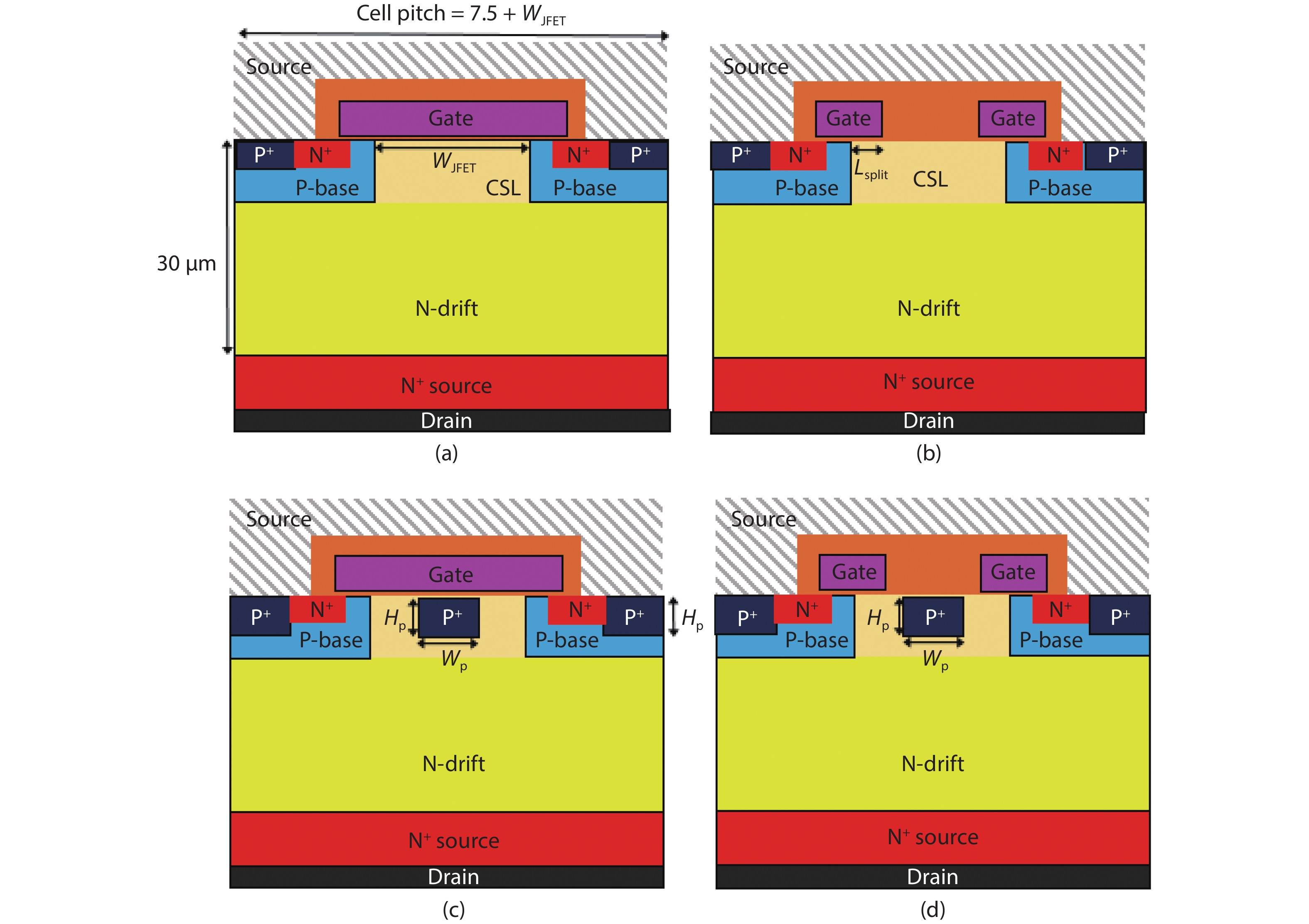
Fig. 1. (Color online) Schematic cross-sectional views of the MOSFETs. (a) Planar MOSFET. (b) SG-MOSFET. (c) CIMOSFET. (d) SG-CIMOSFET.
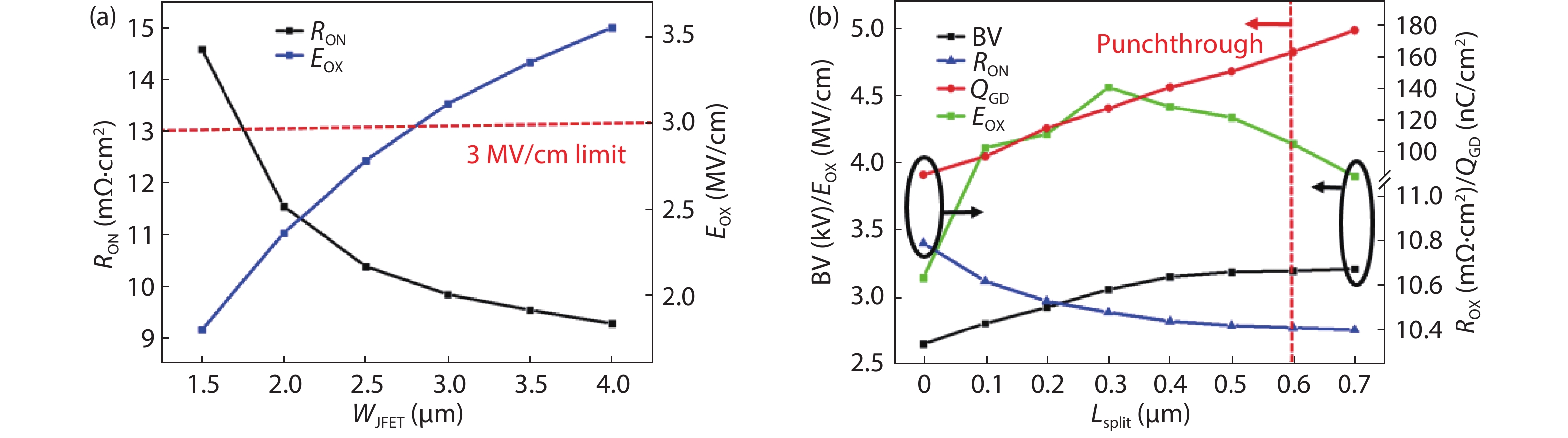
Fig. 2. (Color online) (a) E OX and R ON changes of the planar MOSFET according to the W JFET, and (b) influence of the L split on BV, R ON, Q GD and E OX in SG-MOSFET. BV is extracted at V GS = 0 V and I DS = 1 μ A/cm2.
Fig. 3. (Color online) Electron current density distribution when breakdown occurs in the SG-MOSFET (a) when L split = 0.5 μ m, and (b) when L split = 0.6 μ m.
Fig. 4. (Color online) (a) R ON and BV relation in the SG-CIMOSFET according to change in W P and H P. (b)–(d) Impact ionization position when breakdown occurs in the SG-CIMOSFET according to change in W P and H P (the arrow indicates the breakdown point).
Fig. 5. (a) E OX changes and (b) Q GD changes in the SG-CIMOSFET according to change in W P and H P. E OX is obtained at V DS = 3000 V and V GS = 0 V.
Fig. 6. The I–V characteristics of the four devices. R ON and saturation current is obtained for V GS = 20 V. BV is extracted at V GS = 0 V and I DS = 1 μ A/cm2.
Fig. 7. (Color online) Off-state electric field distributions of the four devices when V GS = 0 V and V DS = 3000 V.
Fig. 8. (Color online) The band diagram in the channel of the four devices at V DS = 0 V, V DS = 3000 V in off-state.
Fig. 9. (Color online) (a) Reverse transfer capacitance characteristics (C RSS) of the five devices. (b) Input capacitance (C ISS) and drain source capacitance (C DS) characteristics of the five devices (when V GS = 0 V, AC signal of 1 MHz).
Fig. 10. (Color online) (a) Depletion lines and reverse transfer capacitance models of the five devices when V DS = 0 V, V GS = 0 V. (b) Depletion lines of the five devices when V DS = 800 V, V GS = 0 V. The solid black line represents the depletion layer.
Fig. 11. Gate charge characteristics and test circuit of the four devices.
Fig. 12. Switching waveforms of the four devices. The active areas of all DUT are set to 1 cm2.
Fig. 13. (Color online) (a) Double pulse test circuit. (b) Switching energy loss diagrams of the four devices.
Fig. 14. (Color online) Proposed fabrication procedure of SG-CIMSOFET. (a) N-type epitaxial growth. (b) Form the base and N+ source region. (c) Form the P+ base and central implant region by tilt ion implantation. (d) Thermal oxidation. (e) Polysilicon deposition. (f) Polysilicon etching. (g) ILD oxide deposition and contact hole etching. (h) Metallization to form the source and drain.
| ||||||||||||||||||||||||||||||||||||||||||||||||||||||||||||||||||||||||||||||||||||||||||
Table 1. Device characteristics comparison.
| ||||||||||||||||||||||||||||||||||||||||||||||||||||||||||||||||||
Table 2. Switching characteristics comparison.

Set citation alerts for the article
Please enter your email address
© Copyright 2018-2021 | Chinese Laser Press. All Rights Reserved 沪ICP备15018463号-20