
Jongwoon Yoon, Kwangsoo Kim. A 3.3 kV 4H-SiC split gate MOSFET with a central implant region for superior trade-off between static and switching performance[J]. Journal of Semiconductors, 2021, 42(6): 062803
- Journal of Semiconductors
- Vol. 42, Issue 6, 062803 (2021)
Abstract
1. Introduction
Silicon carbide (SiC) is considered to be a promising candidate for power applications, thanks to its superior material properties[
There are many approaches to reduce the CRSS (or QGD) in planar MOSFETs. The most widely known structure is the split gate MOSFET (SG-MOSFET), which splits the gate polysilicon to reduce the gate oxide capacitance (COX). The SG-MOSFET not only has inferior static characteristics compared to that of the planar MOSFET, but also has a problem that the electric field is concentrated in the gate corner. As a result, the concentrated electric field concentrated at the gate corner can lead to punch through problems[
A novel 3.3 kV split gate MOSFET with a central implant region (SG-CIMOSFET) is proposed and analyzed in comparison with the planar MOSFET, SG-MOSFET and CIMOSFET. Because of the high drain bias voltage in the 3.3 kV class, the SG-MOSFET does not guarantee the 3 MV/cm oxide limit. In addition, the SG-MOSFET suffers from issues such as punch through and drain-induced barrier lowering (DIBL), which make it more difficult to design. However, the SG-CIMOSFET blocks the oxide electric field by introducing a central implant region in the JFET region and resolves all these issues of the SG-MOSFET. Like the CIMOSFET, the SG-CIMOSFET can significantly reduce the RON because of the high drift doping concentration. By applying the split gate structure and grounded central implant region, the COX and bulk depletion capacitance (Cdep) of the SG-CIMOSFET are reduced simultaneously. In addition, the grounded central implant region partially screens the gate-to-drain capacitive coupling as seen in the CIMOSFET, resulting in the lowest CRSS in spite of the high drift concentration. Since the gate is not directly in contact with the central implant region, the CISS can be reduced significantly compared to that of the CIMOSFET. As a result, the SG-CIMOSFET has the best high frequency figure of merit (HF-FOM) in terms of RON×QGD, RON×CRSS, RON×QG and achieving a superior switching time as well as switching loss. Thus, the SG-CIMOSFET boasts a superior trade-off between static and switching performance.
2. Device structure and optimization
This study was conducted by the Sentaurus TCAD tool[
2.1. Device structure and features
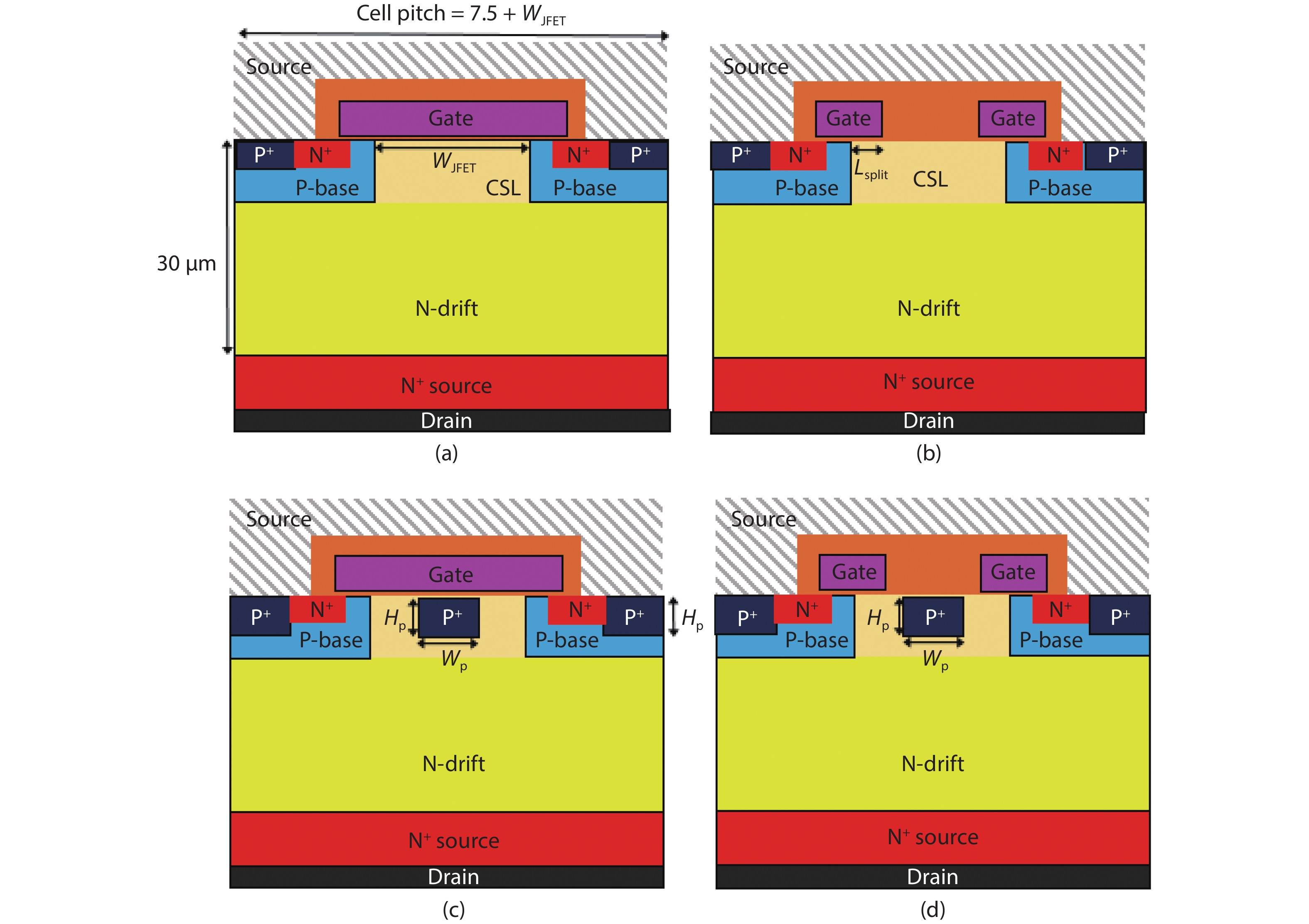
Fig. 1 shows the schematic cross-sectional views of the planar MOSFET, SG-MOSFET, CIMOSFET, and SG-CIMOSFET. In all device structures, the thickness of the 4H-SiC drift layer is 30 μm and the gate oxide thickness is 50 nm. In order to suppress the current flow disturbance resulting from the central implant region in the CIMOSFET and SG-CIMOSFET, a current spreading layer (CSL) with a doping concentration of 2 × 1016 cm–3 is introduced in all structures. The channel length and doping concentration are 0.5 μm and 2 × 1017 cm–3, respectively. A fixed charge concentration of 1 × 1012 cm–2 is included at the SiC/SiO2 interface for all devices. In the CIMOSFET and SG-CIMOSFET, the p+ base and the central implant region is set to same depth to prevent additional mask consumption. The doping concentration of the central implant region is set to 5 × 1018 cm–3.
![]()
Figure 1.(Color online) Schematic cross-sectional views of the MOSFETs. (a) Planar MOSFET. (b) SG-MOSFET. (c) CIMOSFET. (d) SG-CIMOSFET.
2.2. Optimization of each structure
In this optimization process, the drift concentration of all structures starts at 2.2 × 1015 cm–3 to set BV of 3.3 kV in the planar MOSFET. Fig. 2(a) shows the maximum oxide electric field (EOX) and RON changes of the planar MOSFET according to the JFET width (WJFET). EOX is obtained at VDS = 3000 V and VGS = 0 V. As the WJFET decreases, the JFET resistance component increases significantly resulting in a high RON. However, a large WJFET induces a high EOX as it enhances the shielding ability of the p-base. Therefore, WJFET = 2.5 μm (the cell pitch is 10 μm in all structures), which satisfies the 3 MV/cm oxide reliability limit, was adopted in the rest of the study. The relationship between the Lsplit and device characteristics is shown in Fig. 2(b). In Fig. 2(b), when Lsplit is less than 0.4 μm, EOX is obtained when breakdown occurs because BV is less than 3000 V. As the Lsplit decreases so does the QGD. This is due to the decrease in the area between the gate and the drain. Simultaneously, the accumulation resistance increases and the field plate effect of the MOS structure decreases, leading to degradation in the RON and BV[
![]()
Figure 2.(Color online) (a)
![]()
Figure 3.(Color online) Electron current density distribution when breakdown occurs in the SG-MOSFET (a) when
Considering static and switching characteristics, the Lsplit = 0.3 μm was chosen for SG-CIMOSFET and SG-MOSFET in the rest of the study. Fig. 4(a) shows the RON and BV relation in the SG-CIMOSFET according to changes in the central implant width (WP) and height (HP). As WP and HP increase, the depletion region of the JFET region expands and the RON increases. However, the central implant area under the oxide disperses the electric field along with the p-base, greatly reducing the EOX and increasing the BV. When HP is small, the electric field dispersion effect is weak in the central implant region, and impact ionization still occurs in the p-base region (Fig. 4(b)). On the other hand, when HP becomes large (0.6 μm or more), an excessive electric field is concentrated in the central implant region and impact ionization occurs only in the central implant region (Fig. 4(c)). When the WP is 0.8 μm and HP is 0.5 μm, impact ionization occurs simultaneously in the p-base and the central implant region. In this way, the highest BV (3940 V) and BV2/RON of 1281.88 MW/cm2 were obtained as shown in Fig. 4(d). Introduction of the central implant region in the SG-CIMOSFET greatly reduces the maximum oxide field to less than 1.4 MV/cm in all the cases in Fig. 5(a). As a result, punch through is suppressed in SG-CIMOSFET. Therefore, the SG-CIMOSFET can apply a short channel length while suppressing punch through problems when compared to the SG-MOSFET. Fig. 5(b) shows the QGD variation with respect to WP and HP. As the WP and HP increase, QGD becomes smaller because of the depletion expansion. Notably, increasing WP has a greater impact on the decrease of QGD than increasing HP. This is because the grounded central implant region partially screens the capacitive coupling between the gate and the drain as WP increases. Detailed analysis of the capacitance and gate charge characteristics will be covered in the next section. Consequently, the lowest RON×QGD of 418.17 mΩ∙nC and BV2/RON of 1199.79 MW/cm2 were obtained for WP = 0.8 μm and HP = 0.6 μm. However, this study chose to move forward with WP = 0.8 μm and HP = 0.5 μm, which resulted in the best BV2/RON and had an adequately low RON×QGD of 460.18 mΩ∙nC. CIMOSFET also adopted these parameters as it resulted in the best BV2/RON. The CIMOSFET was almost the same BV (3949 V) as the SG-CIMOSFET. However, it has a lower RON (11.19 mΩ∙cm2) than the SG-CIMOSFET (12.11 mΩ∙cm2) due to its accumulation layer resistance. After parameter optimization, the BV of the SG-CIMOSFET and CIMOSFET was set to 3.3 kV by adjusting the drift doping concentration (3 × 1015 cm–3) in order to compare the RON of four devices in the 3.3 kV class.
![]()
Figure 4.(Color online) (a)
![]()
Figure 5.(a)
3. Results and discussions
3.1. Static characteristics
Fig. 6 shows the I–V characteristics of four devices. RON is obtained for VGS = 20 V. BV is extracted at VGS = 0 V and IDS = 1 μA/cm2. The RON of planar MOSFET, SG-MOSFET, CIMOSFET, and SG-CIMOSFET are 10.39, 10.49, 8.59, and 8.67 mΩ∙cm2, respectively. Due to the increased drift doping concentration, CIMOSFET and SG-CIMOSFET were able to significantly improve their RON. Also, the SG-CIMOSFET has nearly the same RON as the CIMOSFET. This is because the current disturbance due to the accumulation resistance is minimized due to the improvement of the drift resistance, which occupies most of the total resistance. The off-state electric field distributions are shown in Fig. 7. Due to the split gate structure of the SG-MOSFET, the electric field is concentrated on the gate edge (EOX = 4.56 MV/cm) and thus the 3 MV/cm reliability limit cannot be met. However, due to the introduction of the central implant region, the electric field is dispersed in the SG-CIMOSFET, reducing the EOX by 2.5 times compared to the planar MOSFET and 4.3 times compared to the SG-MOSFET. CIMOSFET shows the lowest EOX (0.97 MV/cm) but is not significantly different from that of the SG-CIMOSFET (1.06 MV/cm). Fig. 8 shows the band diagram in the channel of the four devices at VDS = 0 V (solid line) and VDS = 3000 V (dotted line). When VDS = 0 V, the band diagram of the four devices is nearly the same because of the same p-base and CSL doping concentration. However, the SG-MOSFET and planar MOSFET show the severe barrier lowering at VDS = 3000 V because of the potential around the channel resulting from the high electric field. The CIMOSFET and SG-CIMOSFET show excellent DIBL suppression due to the electric field shielding of the central implant region.
![]()
Figure 6.The
![]()
Figure 7.(Color online) Off-state electric field distributions of the four devices when
![]()
Figure 8.(Color online) The band diagram in the channel of the four devices at
3.2. Capacitance and gate charge characteristics
For the analysis of the capacitance characteristics, the SG-CIMOSFET with floating central implant region is added to understand the capacitance characteristics. Fig. 9 shows the capacitance characteristics as a function of VDS for the five devices. The CIMOSFET has the largest CISS due to the overlap of the grounded central implant region and the gate. This in turn increases the switching time. In contrast, the SG-CIMOSFET shows a great reduction in CISS compared to the CIMOSFET, due to the separation of the central implant region and gate. In general, the CRSS is expressed by the following equation[
![]()
Figure 9.(Color online) (a) Reverse transfer capacitance characteristics (
where COX is the gate oxide capacitance and Cdep is the bulk depletion capacitance. The SG-MOSFET reduces the CRSS by reducing the COX. But at low VDS, due to its shallow depletion region, the split gate structure induces a large Cdep compared to that of the planar MOSFET, as shown in Fig. 10(a)[
![]()
Figure 10.(Color online) (a) Depletion lines and reverse transfer capacitance models of the five devices when
The gate charge characteristics of the four devices are shown in Fig. 11. The mixed-mode TCAD simulation circuit is shown in the inset of Fig. 11. The QGD is obtained by overlaying the VDS waveform with the gate charge characteristic (measured at 90% of the VDS to 10% of the VDS)[
![]()
Figure 11.Gate charge characteristics and test circuit of the four devices.
Table Infomation Is Not Enable3.3. Switching characteristics
The switching performance analysis of each device are conducted through a double pulse test (DPT) by the mixed-mode TCAD simulation. The active areas of all devices under test (DUT) are set to 1 cm2. Fig. 12 shows the switching waveforms of the four devices. The test circuit for DPT is shown in Fig. 13(a). The body diode of the DUT was used as a freewheeling diode. The gate resistance and stray inductance are set to 20 Ω and 20 nH, respectively. The load inductor is set to 170 μH and the first VGS pulse lasted for 10 μs to yield a load current of 100 A/cm2. The gate voltage is switched between 15 and –5 V. In this paper, the turn-off time (TOFF) consists of two parts, the turn-off delay time (TD-OFF: from 90% of VGS to 10% of VDS) and the turn-off fall time (TF: from 10% of VDS to 90% of VDS). The turn-on time (TON) consists of two parts, the turn-on delay time (TD-ON: from 10% of VGS to 90% of VDS) and the turn-on rise time (TR: from 90% of VDS to 10% of VDS)[
![]()
Figure 12.Switching waveforms of the four devices. The active areas of all DUT are set to 1 cm2.
![]()
Figure 13.(Color online) (a) Double pulse test circuit. (b) Switching energy loss diagrams of the four devices.
Table Infomation Is Not Enable4. Proposed fabrication process
Fig. 14 shows the proposed fabrication procedure of SG-CIMSOFET. After N-type epitaxial growth, the p-base and N+ source region can be formed by ion implantation as shown in Fig. 14(b). In Fig. 4, it shows that the static characteristics of SG-CIMOSFET according to WP and HP are very sensitive. To minimize the sensitivity of parameters, tilt implantation can be used to form the central implant region. The WP and HP can be determined by the implantation parameters[
![]()
Figure 14.(Color online) Proposed fabrication procedure of SG-CIMSOFET. (a) N-type epitaxial growth. (b) Form the base and N+ source region. (c) Form the P+ base and central implant region by tilt ion implantation. (d) Thermal oxidation. (e) Polysilicon deposition. (f) Polysilicon etching. (g) ILD oxide deposition and contact hole etching. (h) Metallization to form the source and drain.
5. Conclusion
In this paper, a novel 3.3 kV class 4H-SiC SG-CIMOSFET is proposed. In the 3.3 kV class, the SG-MOSFET does not guarantee reliable operation due to its high oxide electric field. Moreover, the SG-MOSFET is very vulnerable to the punch through and has been shown to suffer from severe DIBL effect, which makes it more difficult to design devices. The SG-CIMOSFET resolves these problems by applying a central implant region and lowers the EOX by 4.3 times compared to SG-MOSFET. Furthermore, due to its increased drift doping concentration, the SG-CIMOSFET is able to significantly improve RON. In addition, the SG-CIMOSFET significantly lowers the CRSS by partially screening the gate-to-drain capacitive coupling. Compared to the planar MOSFET, the SG MOSFET and the CIMOSFET, the SG-CIMOSFET improves the RON×QGD by 83.7%, 72.4% and 44.5%, respectively. As a result, the SG-CIMOSFET shows the best performance in terms of switching energy loss and switching time. In addition to its simple fabrication process, the SG-CIMOSFET boasts superior trade-off between static and switching performance, making it a promising candidate for high voltage and high frequency applications.
Acknowledgements
This research was supported by the MSIT (Ministry of Science and ICT), Korea, under the ITRC (Information Technology Research Center) support program (IITP-2020-2018-0-01421) supervised by the IITP (Institute for Information & communications Technology Promotion), and then Samsung Electronics.
References
[1] B J. Power MOSFETs Baliga. Fundamentals of power semiconductor devices. Boston, MA: Springer US, 276(2008).
[2] S Q Ji, Z Y Zhang, F Wang. Overview of high voltage sic power semiconductor devices: Development and application. CES Trans Electr Mach Syst, 1, 254(2017).
[3] J A Cooper, A Agarwal. SiC power-switching devices-the second electronics revolution. Proc IEEE, 90, 956(2002).
[4] G Y Wang, F Wang, G R Magai et al. Performance comparison of 1200V 100A SiC MOSFET and 1200V 100A silicon IGBT. 2013 IEEE Energy Convers Congr Expo, 3230(2013).
[5] T Nakamura, Y Nakano, M Aketa et al. High performance SiC trench devices with ultra-low
[6] M Sampath, D T Morisette, J A Cooper. Comparison of single- and double-trench UMOSFETs in 4H-SiC. Mater Sci Forum, 924, 752(2018).
[7] S Krishnaswami, M Das, B Hull et al. Gate oxide reliability of 4H-SiC MOS devices. 2005 IEEE International Reliability Physics Symposium, 592(2005).
[8] S M Xu, C H Ren, Y C Liang et al. Theoretical analysis and experimental characterization of the dummy-gated VDMOSFET. IEEE Trans Electron Devices, 48, 2168(2001).
[9] A Agarwal, K Han, B J Baliga. 2.3 kV 4H-SiC accumulation-channel split-gate planar power MOSFETs with reduced gate charge. IEEE J Electron Devices Soc, 8, 499(2020).
[10] K Han, B J Baliga, W Sung. A novel 1.2 kV 4H-SiC buffered-gate (BG) MOSFET: Analysis and experimental results. IEEE Electron Device Lett, 39, 248(2018).
[11] P Vudumula, S Kotamraju. Design and optimization of 1.2-kV SiC planar inversion MOSFET using split dummy gate concept for high-frequency applications. IEEE Trans Electron Devices, 66, 5266(2019).
[12] Q C J Zhang, J Duc, B Hull et al. CIMOSFET: A new MOSFET on SiC with a superior
[13] Q J Zhang, G Y Wang, H Doan et al. Latest results on 1200 V 4H-SiC CIMOSFETs with
[14]
[15] M N Darwish, J L Lentz, M R Pinto et al. An improved electron and hole mobility model for general purpose device simulation. IEEE Trans Electron Devices, 44, 1529(1997).
[16]
[17] K Han, B J Baliga, W Sung. Split-gate 1.2-kV 4H-SiC MOSFET: Analysis and experimental validation. IEEE Electron Device Lett, 38, 1437(2017).
[18] J Wei, M Zhang, H P Jiang et al. Low ON-resistance SiC trench/planar MOSFET with reduced OFF-state oxide field and low gate charges. IEEE Electron Device Lett, 37, 1458(2016).
[19] J Wei, M Zhang, H P Jiang et al. Dynamic degradation in SiC trench MOSFET with a floating p-shield revealed with numerical simulations. IEEE Trans Electron Devices, 64, 2592(2017).
[20] M Ren, Z Chen, B Niu et al. A low miller capacitance VDMOS with shield gate and oxide trench. 2016 IEEE International Nanoelectronics Conference (INEC), 1(2016).
[21] T Basler, D Heer, D Peters et al. Practical aspects and body diode robustness of a 1200 V SiC trench MOSFET. International Exhibition and Conference for Power Electronics, Intelligent Motion, Renewable Energy and Energy Management, 1(2018).
[22] A Maerz, T Bertelshofer, M Bakran et al. A novel gate drive concept to eliminate parasitic turn-on of SiC MOSFET in low inductance power modules. International Exhibition and Conference for Power Electronics, Intelligent Motion, Renewable Energy and Energy Management, 1(2017).
[23] K Tian, A Hallén, J W Qi et al. An improved 4H-SiC trench-gate MOSFET with low ON-resistance and switching loss. IEEE Trans Electron Devices, 66, 2307(2019).
[24] T Morikawa, T Ishigaki, A Shima. Device design consideration for robust SiC VDMOSFET with self-aligned channels formed by tilted implantation. IEEE Trans Electron Devices, 66, 3447(2019).
[25] X T Zhou, R F Yue, J Zhang et al. 4H-SiC trench MOSFET with floating/grounded junction barrier-controlled gate structure. IEEE Trans Electron Devices, 64, 4568(2017).


Set citation alerts for the article
Please enter your email address

© Copyright 2018-2021 | Chinese Laser Press. All Rights Reserved 沪ICP备15018463号-20