
Shujie Pan, Victoria Cao, Mengya Liao, Ying Lu, Zizhuo Liu, Mingchu Tang, Siming Chen, Alwyn Seeds, Huiyun Liu. Recent progress in epitaxial growth of III–V quantum-dot lasers on silicon substrate[J]. Journal of Semiconductors, 2019, 40(10): 101302
- Journal of Semiconductors
- Vol. 40, Issue 10, 101302 (2019)
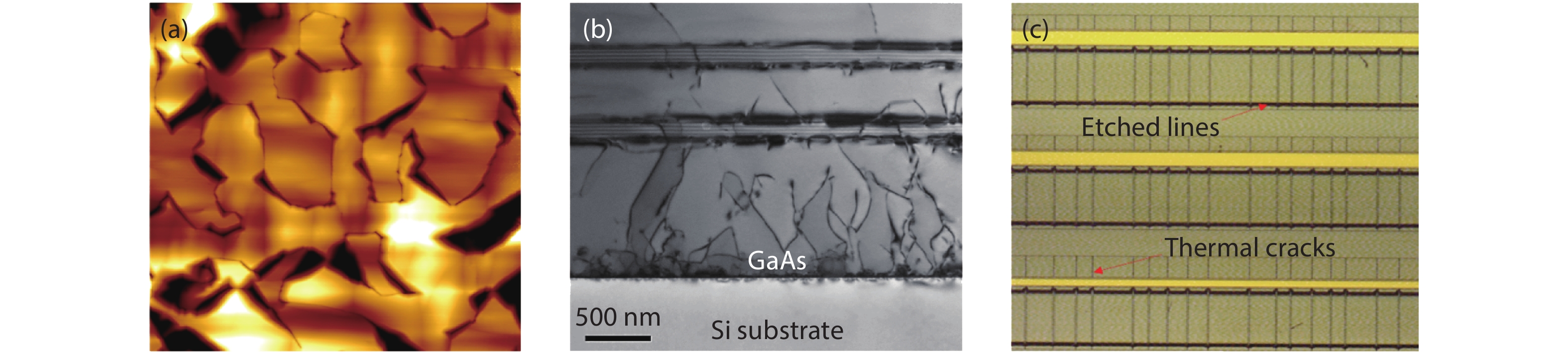
Fig. 1. (Color online) Three major issues faced in monolithic III–V/Si integration: (a) APBs, (b) TDs and (c) thermal cracks.
![(Color online) (a) Schematic illustration of the comparative interaction of threading dislocations with QWs and QDs. (b) Cross-sectional schematic description of the mechanism of dislocation bending by QDs. (c) Bright-field scanning transmission electron microscopy (TEM) images of the TDs in the QD active region[11]. Copyright © 2016, Springer Nature. With permission of Springer (c). © 2009, IEEE. Reprinted with permission from Ref. [39] (b).](/richHtml/jos/2019/40/10/101302/img_2.jpg)
Fig. 2. (Color online) (a) Schematic illustration of the comparative interaction of threading dislocations with QWs and QDs. (b) Cross-sectional schematic description of the mechanism of dislocation bending by QDs. (c) Bright-field scanning transmission electron microscopy (TEM) images of the TDs in the QD active region[11 ]. Copyright © 2016, Springer Nature. With permission of Springer (c). © 2009, IEEE. Reprinted with permission from Ref. [39 ] (b).
Fig. 3. (Color online) (a) Dark-field scanning TEM image of a Si substrate with 4° off-cut. (b) High resolution high-angle annular dark-field scanning TEM image of the 6 nm-thick AlAs nucleation layer between GaAs buffer layer and a Si substrate. (c) Bright-field scanning TEM image of DFLs. (d) Bright-field scanning TEM image of the QD active layers. (e) Photoluminescence (PL) spectrum of a QD active region grown on GaAs and Si. (f) Cross-sectional scanning emission microscopy (SEM) image of the fabricated RWG laser with as-cleaved facets. Copyright © 2016, Springer Nature. With permission of Springer (a–c). Reprinted with permission from Ref. [49 ], The Optical Society (OSA), CC BY 4.0 (d–f).
Fig. 4. (Color online) (a) Measured RT CW L –I –V curves for a 50 μ m × 3200 μ m InAs/GaAs QD laser grown on a Si substrate. (b) Ageing data for the InAs/GaAs QD laser under CW (drive current = 210 mA) at a constant heat sink temperature of 26 °C. (c) Measured CW L–I curve from a 2.2 μ m × 4 mm narrow-ridge-waveguide laser as a function of temperature. (d) Lateral near-field intensity profiles with different injection currents. Inset: infrared (IR) camera image of lasing near-field at the threshold of 20 mA (well above threshold). (e) RIN spectra up to 16 GHz at gain currents of 40, 60 and 80 mA. (f) Experimental results. Left: 25.6 Gb/s eye-diagrams at back-to-back and after transmission over 13 km SMF28. Right: measured bit-error rate (BER) results at different received power. Copyright © 2016, Springer Nature. With permission of Springer (a and b). Reprinted with permission from Ref. [49 ], The Optical Society (OSA), CC BY 4.0 (c–f).
Fig. 5. (Color online) (a) Cutaway schematic of the DFB laser array on Si (not to scale). (b) High-resolution SEM image of the gratings with a λ /4 phase shift in the middle of the etched gratings. (c) The L–I–V curve of a single 1 mm long Si-based DFB laser. (d) Optical spectra of a DFB laser array with different grating periods around their maximum output power levels before saturation at RT. Reprinted with permission from Ref. [56 ], The Optical Society (OSA).
Fig. 6. (Color online) (a) Schematic of layer structure of QD MD laser on Si. The insets are an SEM image of a cross-section of the structure (left) and a TEM image of the QD active region (right). (b) The RT CW L–I–V curve for a 25 μ m × 3 mm Si-based edge-emitting QD laser. The inset shows an atomic force microscopy (AFM) image of an uncapped Si-based QD sample. (c) RT CW emission spectrum measured at a current of ~ 1.4 × threshold for MD-on-Si lasers with diameters of 14 and 30 μ m. Dashed curve: PL spectrum of QD material (not in scale). The inset: an SEM image of the MD laser (D = 30 μ m). Reprinted with permission from Ref. [61 ], The Optical Society (OSA).
Fig. 7. Bright-field scanning TEM image of on-axis Si (001) substrate.
Fig. 8. (Color online) (a) Single-facet output power versus current density for the same Si-based InAs/GaAs QD laser as a function of temperature under CW operation. The inset shows the L–I curve for this Si-based InAs/GaAs QD laser at a heat sink temperature of 36 °C. (b) Single-facet light power verses current density for an InAs/GaAs QD laser grown on GaAs/Si (001) substrate at various heat sink temperatures under pulsed condition. The inset shows the natural logarithm of current density against temperature in the ranges of 16–102 °C. (c) Measured L–I–V curve of 50 μ m × 3 mm broad-area InAs/GaAs QD laser directly grown on GaAs/Si (001) substrate. (d) Measured L–I curve of InAs/GaAs QD laser directly grown on GaAs/Si (001) as a function of temperature. Inset: lasing spectrum at 180 A/cm2 injection current density. Reprinted with permission from Ref. [68 ], CC BY 4.0 (a and b). Reprinted with permission from Ref. [69 ], CC BY 4.0 (c and d).
Fig. 9. (Color online) (a) Schematic diagram of a microdisk laser grown on planar on-axis Si (001) substrate. (b) SEM image of a fabricated microdisk laser. (c) Collected PL spectra above and below the lasing threshold of a MD with D ~ 1.9 μ m. Reprinted with Permission from Ref. [70 ], The Optical Society (OSA).

Set citation alerts for the article
Please enter your email address
© Copyright 2018-2021 | Chinese Laser Press. All Rights Reserved 沪ICP备15018463号-20