
Shujie Pan, Victoria Cao, Mengya Liao, Ying Lu, Zizhuo Liu, Mingchu Tang, Siming Chen, Alwyn Seeds, Huiyun Liu. Recent progress in epitaxial growth of III–V quantum-dot lasers on silicon substrate[J]. Journal of Semiconductors, 2019, 40(10): 101302
- Journal of Semiconductors
- Vol. 40, Issue 10, 101302 (2019)
Abstract
1. Introduction
For decades, with increasing research in the silicon (Si) microelectronics industry, the exponentially increasing complexity of integrated circuits (ICs) has been witnessed. The capabilities of interconnects have become an essential role in evaluating chip performance, especially for the very large-scale integration (VLSI). This results in the urgent demand for achieving cost-effective and high-performance integrated photonics devices. The superior properties of Si, including low-defect density, high thermal conductivity and high refractive-index contrast between Si and its native oxide i.e. SiO2 raise the potential for scalable Si photonic integrated circuits (PICs). Thus far, the Si community has well-developed many photonics building blocks, including ultra-fast modulators[
This review paper began by reviewing the challenges of monolithic growth of Si-based III–V compounds. Then, the advantages of QDs for monolithic III–V/Si integration technology were discussed. Followed by our recent progress being made in achieving high-performance O-band InAs QD lasers monolithically growth of III–V QD lasers on both off cut and on-axis Si platforms.
2. Challenges in monolithic growth
Ever since the first attempt to grow GaAs thin films on Si-substrates in the 1980s[
![]()
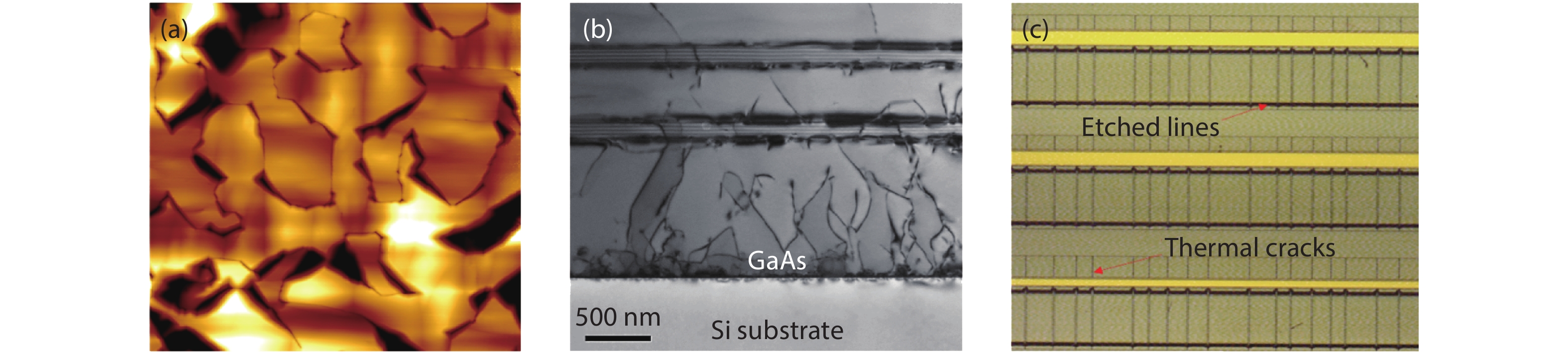
Figure 1.(Color online) Three major issues faced in monolithic III–V/Si integration: (a) APBs, (b) TDs and (c) thermal cracks.
The first issue shown in Fig. 1(a) is related to the formation of the APBs in III–V/Si epitaxy, which comes from the combination of polar and non-polar bonds. In practice, the Si (001) surface always contains single atomic steps, and the nucleation of the group V species on the Si surface always emerges preferentially over the group III species. Single atomic steps will induce planes of III–III and V–V bonds separately[
The second issue is the formation of the TDs. Compared to Si, whose lattice constant is 5.431, GaAs (5.653) has approximately 4% lattice mismatch. This leads to continuous stress accumulation in the epilayer, and this stacked energy will be released at the pseudomorphic critical point with increasing deposition thickness. This relaxation will cause two types of dislocations: misfit dislocations and TDs. Neither of the dislocations can terminate within a crystal due to the energetic reasons; they must either stop at the edge as misfit dislocations or propagate upwards to form the TDs[
The last issue is that of thermal cracks, which normally appears during the cooling-down process from high growth temperature (normally ~600 °C) to room temperature (RT). It originates from the different thermal expansion coefficient between III–V and Si material, which promotes the accumulative thermal strain in the epilayer. The strain relaxation results in cracks formed in the III–V film and this will seriously reduce the performance and the yield of the device. Moreover, it will limit the maximum achievable growth thickness of III–V compounds on Si. In addition to cracks, this thermal strain may create an extra driving force for dislocation growth and further degrade devices’ performance[
3. Advantages of quantum dots (QDs)
After the hypothetical heterojunction structures proposed by Kroemer in 1963[
However, in reality, early QDs devices suffered from QD size fluctuations resulting from the inevitable self-assembly techniques[
![]()
Figure 2.(Color online) (a) Schematic illustration of the comparative interaction of threading dislocations with QWs and QDs. (b) Cross-sectional schematic description of the mechanism of dislocation bending by QDs. (c) Bright-field scanning transmission electron microscopy (TEM) images of the TDs in the QD active region[
4. QD lasers on Si substrate with off cut
In the last few years, unbelievable developments have been witnessed in Si photonics: the increasing functionality in Si-based integrated circuits (IC) and the excellent performance of most key optical components. Based on these achievements, many efforts have been devoted to fabricating efficient Si-based lasers which are indispensable to the phonics integrated circuits (PICs), and much progress has been made. In spite of that, the very first QD laser monolithically grown on Si was reported in 1999[
A few epitaxial growth techniques were used to minimise the impact of various defects and the general Si off cut substrate developed by the UCL group can be found in Fig. 3. The design of the 4° off-cut angle could eliminate the formation of APBs. At the initial stage, a thin AlAs nucleation layer was employed to suppress 3-D growth and provided a flat interface for the following depositions[
![]()
Figure 3.(Color online) (a) Dark-field scanning TEM image of a Si substrate with 4° off-cut. (b) High resolution high-angle annular dark-field scanning TEM image of the 6 nm-thick AlAs nucleation layer between GaAs buffer layer and a Si substrate. (c) Bright-field scanning TEM image of DFLs. (d) Bright-field scanning TEM image of the QD active layers. (e) Photoluminescence (PL) spectrum of a QD active region grown on GaAs and Si. (f) Cross-sectional scanning emission microscopy (SEM) image of the fabricated RWG laser with as-cleaved facets. Copyright © 2016, Springer Nature. With permission of Springer (a–c). Reprinted with permission from Ref. [
In this section, a few representative off cut Si-based QD lasers fabricated using the above growth techniques will be reviewed, including the Fabry-Perot (FP) laser, the narrow-ridge-waveguide (RWG) FP laser, the distributed feedback (DFB) laser and the micro-disk laser, all on off cut Si substrate.
4.1. FP lasers on off cut Si substrate
A pioneering work was done by Chenet al. in 2016[
![]()
Figure 4.(Color online) (a) Measured RT CW
Later, the broad-area lasers described in Ref. [11] were used to generate the first gain-switched optical pulses. Their dynamic properties for optical communications have been studied in both experimental and theoretical ways, and good agreement could be found between the two. The typical time duration for the shortest pulses observed is between 175 and 200 ps, with a maximum peak output power of up to 66 mW. A trade-off between maximising the optical power and narrowing the pulse duration has been noticed: a longer high-amplitude drive pulse results in a higher peak optical power, while a shorter one can provide us with a narrower pulse width. Simulations and analysis suggest that there are two main reasons for the broadened pulse width: a limited gain from InAs QDs and a high gain compression factor. Therefore, it is believed that the optical applications of Si-based QD lasers could be significantly improved by increasing the number of active layers, introducing the p-doping in the active region as well as modifying the devices’ geometry[
Because the multi-transverse-mode operation might limit the laser’s dynamic response, the RWG FP lasers with 2.2 μm ridge width were then fabricated to ensure the single-transverse mode lasing at 1.3 μm. In additions, these RWG lasers could help us to take a closer step towards practical applications in tele-/data communications. Depicted in Figs. 4(c)–4(f), the designed RWG QD lasers have a CW threshold current as low as 12.5 mA at RT, and it could operate at up to 90 °C under CW. In addition, an ultra-low relative intensity noise (RIN) (< –150 dB/Hz) was measured in the range of 4–16 GHz. Based on these excellent noise characteristics, 25.6 Gb/s data transmission over 13.5 km SMF-28 has been demonstrated[
Soon after, a comprehensive study was carried out on a 2.5 mm long RWG QD lasers. The small-signal modulation unveils the maximum 3 dB bandwidths of 1.6 GHz with the value of D-factors value equals to 0.3 GHz/mA1/2, K-factors in the range of 2.4 to 3.7 ns and the modulation current efficiencies of 0.4 GHz/mA1/2. A simulation of small-signal response was also applied to reveal the optimised device geometry: a 0.75 mm long cavity with 99% and 60% high-reflection coatings and ten QD layers, which forecast a maximum 3 dB-modulation bandwidth of 5 GHz to 7 GHz[
4.2. Distributed-feedback (DFB) lasers on off cut Si substrate
The excellent Si-based III–V FP laser sources with specially designed cavities could implement single-mode lasers, and this will enable wavelength division multiplexing (WDM), which is necessary in high-performance applications[
![]()
Figure 5.(Color online) (a) Cutaway schematic of the DFB laser array on Si (not to scale). (b) High-resolution SEM image of the gratings with a
As a result, the first Si-based electrically pumped single-mode DFB laser array using InAs/GaAs QD gain materials was demonstrated, which could lase at RT under CW. The threshold current of this device was as low as 12 mA, and its single-mode side mode suppression ratio (SMSR) was as high as 50 dB[
4.3. Micro-lasers on off cut Si substrate
Not only macro-lasers but also micro-lasers show great potential to work as a long-wavelength light source for Si photonics owing to their short cavity length, small size and low power consumption[
In 2017, Kryzhanovskaya et al. succeeded in demonstrating the first Si-based micro-disk lasers with diameters from 14 to 30 μm and enabled emission in the range of 1320–1350 nm with minima Jth of 600 A/cm2[
![]()
Figure 6.(Color online) (a) Schematic of layer structure of QD MD laser on Si. The insets are an SEM image of a cross-section of the structure (left) and a TEM image of the QD active region (right). (b) The RT CW
5. QD lasers on on-axis Si (001) substrate
Even though, the off cut Si substrate could inhibit the emergence of APBs, adopting the ‘exact’ (001) Si substrates (shown in Fig. 7) is an essential step to fully exploit the potential of Si photonics because of its compatibility with conventional CMOS processing[
![]()
Figure 7.Bright-field scanning TEM image of on-axis Si (001) substrate.
In this section, our recent achievements in FP and MD QD lasers with on-axis Si (001) substrate will be covered.
5.1. FP lasers on on-axis Si substrate
The first CW electrically pumped InAs/GaAs QD lasers monolithically grown on ‘exact’ (001) Si substrate were reported by Chen et al. from UCL in 2017, in which no intermediate buffer layers or patterned Si substrates were used[
![]()
Figure 8.(Color online) (a) Single-facet output power versus current density for the same Si-based InAs/GaAs QD laser as a function of temperature under CW operation. The inset shows the
By optimising the growth conditions, Li et al. achieved a high-quality electrically pumped on-axis Si-based QD laser with low threshold current density (160 A/cm2 @ RT CW). Moreover, the lasing was observed at up to 52 °C under CW[
5.2. Micro-lasers on on-axis Si substrate
Recently, Zhou et al. have developed a CW optically pumped InAs/GaAs QD MD directly grown on on-axis Si (001) substrate[
Fig. 9 displays the schematic diagram of the MD laser together with its SEM image. The lasing characteristics of the fabricated device with small diameter (D) in the range of 1.1–2 μm are demonstrated. According to the measurements, lasing emission from both ground states and excited states were obtained with an ultra-low lasing threshold of ~ 3 μW (for D ~ 1.1 μm)[
![]()
Figure 9.(Color online) (a) Schematic diagram of a microdisk laser grown on planar on-axis Si (001) substrate. (b) SEM image of a fabricated microdisk laser. (c) Collected PL spectra above and below the lasing threshold of a MD with
6. Conclusion
This paper has predominantly reviewed the recent achievements made by UCL in the epitaxial growth of various III–V QD lasers monolithically grown on Si substrates, including the FP laser, the DFB laser and the MD laser. We also discuss material dissimilarity issues between the III–V compounds and Si substrates, which will generate different kinds of defects and seriously hinder the development of Si photonics. The 3-D confined island-structure with discrete energy levels has captured plenty of attention since first realised in 1994 due to its irreplaceable properties in temperature stability and defects immunisation. To obtain a high-performance device, numerous growth techniques have been investigated worldwide, such as the nucleation layers, the dislocation filter layers and the in situ thermal annealing process.
Owing to these intense research efforts, 1.3 μm InAs QD lasers monolithically grown on Si (001) substrate with a 4° off-cut towards the [011] plane have achieved impressive results: the FP laser with ultra-low threshold current density (62.5 A/cm2) and incredibly long life-time (over 100,158 h), the narrow-ridge-waveguide FP laser with excellent noise characteristics (RIN < –150 dB/Hz), and the first electrically pumped DFB laser together with the first Si-based micro-disk laser. However, lasing from the on-axis Si (001) substrate is needed to take advantages of the well-developed CMOS industry. Our group succeeded in realising the first CW electrically pumped InAs/GaAs QD lasers monolithically grown on the on-axis Si (001) substrate lasing up to 102 °C (pulsed) in 2017. Soon after, an improved version was exhibited with a threshold current density of 160 A/cm 2 (@ RT CW) and lasing up to 52 °C under CW mode. Moreover, a MD laser directly grown on ‘exact’ Si (001) substrate was obtained recently with a lasing threshold as low as 3 μW.
These remarkable accomplishments confirm that the monolithic Si-based QD laser is a promising candidate for integrating the optoelectronics devices with Si platforms and prove the feasibility to fully explore the applications of Si photonics.
Acknowledgements
The authors acknowledge financial support from the UK EPSRC under grant No. EP/P006973/1, and the EPSRC National Epitaxy Facility European project H2020-ICT-PICTURE (780930); the Royal Academy of Engineering (RF201617/16/28) and Investissments d’avenir (IRT Nanoelec: ANR-10-IRT-05 and Need for IoT: ANR-15-IDEX-02). S. Pan and M. Liao thank to the Chinese Scholarship Council for funding their studies. S. Chen acknowledges the Royal Academy of Engineering for funding his Research Fellowship.
References
[1] G T Reed, G Mashanovich, F Y Gardes et al. Silicon optical modulators. Nat Photonics, 4, 518(2010).
[2] X Xiao, H Xu, X Y Li et al. High-speed, low-loss silicon Mach–Zehnder modulators with doping optimization. Opt Express, 21, 4116(2013).
[3] M Streshinsky, R Ding, Y Liu et al. Low power 50 Gb/s silicon traveling wave Mach-Zehnder modulator near 1300 nm. Opt Express, 21, 30350(2013).
[4] O I Dosunmu, D D Can, M K Emsley et al. High-speed resonant cavity enhanced Ge photodetectors on reflecting Si substrates for 1550-nm operation. IEEE Photonics Technol Lett, 17, 175(2005).
[5] T Yin, R Cohen, M M Morse et al. 31 GHz Ge n–i–p waveguide photodetectors on silicon-on-insulator substrate. Opt Express, 15, 13965(2007).
[6] L Vivien, A Polzer, D Marris-Morini et al. Zero-bias 40 Gbit/s germanium waveguide photodetector on silicon. Opt Express, 20, 1096(2012).
[7] J F Bauters, M L Davenport, M J R Heck. Silicon on ultra-low-loss waveguide photonic integration platform. Opt Express, 21, 544(2013).
[8] M J R Heck, J F Bauters, M L Davenport et al. Ultra-low loss waveguide platform and its integration with silicon photonics. Laser Photon Rev, 8, 667(2014).
[9] H Y Liu, T Wang, Q Jiang et al. Long-wavelength InAs/GaAs quantum-dot laser diode monolithically grown on Ge substrate. Nat Photonics, 5, 416(2011).
[10] D Liang, J E Bowers. Recent progress in lasers on silicon. Nat Photonics, 4, 511(2010).
[11] S Chen et al. Electrically pumped continuous-wave III–V quantum dot lasers on silicon. Nat Photonics, 10, 307(2016).
[12] K Tanabe, K Watanabe, Y Arakawa. III–V/Si hybrid photonic devices by direct fusion bonding. Sci Rep, 2349(2012).
[13] E Tournié, L Cerutti, J B Rodriguez et al. Metamorphic III–V semiconductor lasers grown on silicon. MRS Bull, 41, 218(2016).
[14] R Fischer, W T Masselink, J Klem et al. Growth and properties of GaAs/AlGaAs on nonpolar substrates using molecular beam epitaxy. J Appl Phys, 58, 374(1985).
[15] W I Wang. Molecular beam epitaxial growth and material properties of GaAs and AlGaAs on Si (100). J Appl Phys, 44, 1149(1984).
[16] Q Li, M Lau. Epitaxial growth of highly mismatched III–V materials on (001) silicon for electronics and optoelectronics. Prog Cryst Growth Charact Mater, 63, 105(2017).
[17] R Alcotte, M Martin, J Moeyaert et al. Epitaxial growth of antiphase boundary free GaAs layer on 300 mm Si(001) substrate by metalorganic chemical vapour deposition with high mobility. APL Mater, 4, 46101(2016).
[18] M Akiyama, Y Kawarada, K Kaminishi. Growth of single domain gaas layer on (100)-oriented Si substrate by MOCVD. Jpn J Appl Phys, 23, L843(1984).
[19] J C Norman, D Jung, Y Wan et al. Perspective: The future of quantum dot photonic integrated circuits. APL Photonics, 3, 30901(2018).
[20] J Wu, S Chen, A Seeds et al. Quantum dot optoelectronic devices: lasers, photodetectors and solar cells. J Phys D, 48, 363001(2015).
[21]
[22] H Kroemer. A proposed class of hetero-junction injection lasers. Proc IEEE, 51, 1782(1963).
[23] Z I Alferov. AlAs–GaAs heterojunction injection lasers with a low room-temperature threshold. Sov Phys Semicond, 3, 1107(1970).
[24]
[25] E Kapon, S Simhony, R Bhat et al. Single quantum wire semiconductor lasers. Appl Phys Lett, 55, 2715(1989).
[26] Y Arakawa, H Sakaki. Multidimensional quantum well laser and temperature dependence of its threshold current. Appl Phys Lett, 40, 939(1982).
[27] N Kirstaedter, N N Ledentsov, M Grundmann et al. Low threshold, large To injection laser emission from (InGa)As quantum dots. Electron Lett, 30, 1416(1994).
[28] K Nishi, K Takemasa, M Sugawara et al. Development of quantum dot lasers for data-com and silicon photonics applications. IEEE J Sel Top Quantum Electron, 23, 1(2017).
[29] K Nishi, T Kageyama, M Yamaguchi et al. Molecular beam epitaxial growths of high-optical-gain InAs quantum dots on GaAs for long-wavelength emission. J Cryst Growth, 378, 459(2013).
[30] B Ilahi, M Souaf, M Baira et al. Evolution of InAs/GaAs QDs size with the growth rate: a numerical investigation. J Nanomater, 2015, 1(2015).
[31] D Leonard, S Fafard, K Pond et al. Structural and optical properties of self-assembled InGaAs quantum dots. J Vac Sci Technol B, 12, 2516(1994).
[32] K Nishi, H Saito, S Sugou et al. A narrow photoluminescence linewidth of 21 meV at 1.35
[33] K Otsubo, N Hatori, M Ishida et al. Temperature-insensitive eye-opening under 10-Gb/s modulation of 1.3-
[34] K Takada, Y Tanaka, T Matsumoto et al. Wide-temperature-range 10.3 Gbit/s operations of 1.3 μm high-density quantum-dot DFB lasers. Electron Lett, 47, 206(2011).
[35] A Capua et al. Direct correlation between a highly damped modulation response and ultra low relative intensity noise in an InAs/GaAs quantum dot laser. Opt Express, 15, 5388(2007).
[36] D Jung, Z Zhang, J Norman et al. Highly reliable low-threshold inas quantum dot lasers on on-axis (001) Si with 87% injection efficiency. ACS Photonics, 5, 1094(2018).
[37] I Ovid’ko. Relaxation mechanisms in strained nanoislands. Phys Rev Lett, 88, 46103(2002).
[38] K Tillmann, A Förster. Critical dimensions for the formation of interfacial misfit dislocations of In0.6Ga0.4As islands on GaAs(001). Thin Solid Films, 368, 93(2000).
[39] Z Mi, J Yang, P Bhattacharya et al. High-performance quantum dot lasers and integrated optoelectronics on Si. Proc IEEE, 97, 1239(2009).
[40] B Shi, Q Li, K M Lau. Self-organized InAs/InAlGaAs quantum dots as dislocation filters for InP films on (001) Si. J Cryst Growth, 464, 28(2017).
[41] K Linder, J Phillips, O Qasaimeh et al. Self-organized In0.4Ga0.6As quantum-dot lasers grown on Si substrates. Appl Phys Lett, 70, 1355(1999).
[42] T Wang, H Liu, A Lee et al. 1.3-
[43] A D Lee, Q Jiang, M C Tang et al. InAs/GaAs quantum-dot lasers monolithically grown on Si, Ge, and Ge-on-Si substrates. IEEE J Sel Top Quantum Electron, 19, 1901107(2013).
[44] S M Chen, M Tang, J Wu et al. 1.3-
[45] J R Orchard, S Shutts, A Sobiesierski et al. In situ annealing enhancement of the optical properties and laser device performance of InAs quantum dots grown on Si substrates. Opt Express, 24, 6196(2016).
[46] Q Jiang, M C Tang, J Wu et al. 1.3
[47] M Liao, S Chen, J S Park et al. III–V quantum-dot lasers monolithically grown on silicon. Semicond Sci Technol, 33, 123002(2018).
[48] M Tang, S M Chen, J Wu et al. Optimizations of defect filter layers for 1.3-
[49] M Liao, S M Chen, Z X Liu et al. Low-noise 13
[50] C Hantschmann, P P Vasil'ev, S M Chen et al. Gain switching of monolithic 1.3
[51] C Hantschmann, P P Vasil’ev, A Wonfor et al. Understanding the bandwidth limitations in monolithic 1.3
[52]
[53] C Merckling, N Waldron, S Jiang et al. Heteroepitaxy of InP on Si(001) by selective-area metal organic vapor-phase epitaxy in sub-50 nm width trenches: The role of the nucleation layer and the recess engineering. J Appl Phys, 115, 23710(2014).
[54] Z Wang, B Tian, M Pantouvaki et al. Room-temperature InP distributed feedback laser array directly grown on silicon. Nat Photonics, 9, 837(2015).
[55] B Tian, Z C Wang, M Pantouvaki et al. Room temperature O-band DFB laser array directly grown on (001) silicon. Nano Lett, 17, 559(2017).
[56] Y Wang, S M Chen, Y Yu et al. Monolithic quantum-dot distributed feedback laser array on silicon. Optica, 5, 528(2018).
[57] H C Kim, J Wiedmann, K Matsui et al. 1.5-
[58] K J Vahala. Optical microcavities. Nature, 424, 839(2003).
[59] M V Maximov, N V Kryzhanovskaya, A M Nadtochiy et al. Ultrasmall microdisk and microring lasers based on InAs/InGaAs/GaAs quantum dots. Nanoscale Res Lett, 9, 657(2014).
[60] N V Kryzhanovskaya, A Z Zhukov, M V Maximov et al. Room temperature lasing in 1-
[61] N Kryzhanovskaya, v A E Zhukov, M V Maximov et al. Heat-sink free CW operation of injection microdisk lasers grown on Si substrate with emission wavelength beyond 13
[62] N Kryzhanovskaya, E Moiseev, Y Polubavkina et al. Elevated temperature lasing from injection microdisk lasers on silicon. Laser Phys Lett, 15, 15802(2018).
[63] K Volz, A Beyer, e W Witte et al. GaP-nucleation on exact Si (001) substrates for III/V device integration. J Cryst Growth, 315, 37(2011).
[64] A Y Liu, J Peters, X Huang et al. Electrically pumped continuous-wave 13
[65] D Jung, Y Song, M Lee et al. InGaAs/GaAs quantum well lasers grown on exact GaP/Si (001). Electron Lett, 50, 1226(2014).
[66] Q Li, K W Ng, K M Lau. Growing antiphase-domain-free GaAs thin films out of highly ordered planar nanowire arrays on exact (001) silicon. Appl Phys Lett, 106, 72105(2015).
[67] Q Li, Y T Wan, A Y Liu et al. 13-
[68] S M Chen, M Y Liao, M C Tang et al. Electrically pumped continuous-wave 1.3
[69] K Li, Z Liu, M Tang et al. O-band InAs/GaAs quantum dot laser monolithically integrated on exact (001) Si substrate. J Cryst Growth, 511, 56(2019).
[70] T J Zhou, M C Tang, G H Xiang et al. Ultra-low threshold InAs/GaAs quantum dot microdisk lasers on planar on-axis Si (001) substrates. Optica, 6, 430(2019).


Set citation alerts for the article
Please enter your email address

© Copyright 2018-2021 | Chinese Laser Press. All Rights Reserved 沪ICP备15018463号-20