
Nasir Alfaraj, Jung-Wook Min, Chun Hong Kang, Abdullah A. Alatawi, Davide Priante, Ram Chandra Subedi, Malleswararao Tangi, Tien Khee Ng, Boon S. Ooi. Deep-ultraviolet integrated photonic and optoelectronic devices: A prospect of the hybridization of group III–nitrides, III–oxides, and two-dimensional materials[J]. Journal of Semiconductors, 2019, 40(12): 121801
- Journal of Semiconductors
- Vol. 40, Issue 12, 121801 (2019)
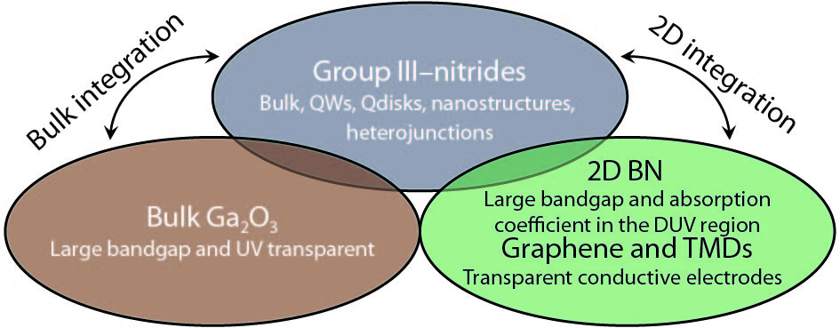
Fig. 1. (Color online) Graphical abstract reflecting areas explored in this review article.
![(Color online) Comparison of donor activation energies of Si-doped AlxGa1−xN obtained experimentally by various research groups[162–165]. Reprinted with permission from Ref. [161]. ©2017, Elsevier.](/richHtml/jos/2019/40/12/121801/img_2.jpg)
Fig. 2. (Color online) Comparison of donor activation energies of Si-doped Alx Ga1−x N obtained experimentally by various research groups[162 –165] . Reprinted with permission from Ref. [161 ]. ©2017, Elsevier.
Fig. 3. (Color online) Variation in Alx Ga1−x N resistivity values as a function of the Si/III ratio[166]. The percentages refer to aluminum mole fraction. Reprinted with permission from Ref. [161 ]. ©2017, Elsevier.
Fig. 4. (Color online) (a) Crystal structure of single layer h-BN. (b) SEM image of h-BN growth on HOPG demonstrating nucleation from HOPG in terrace steps pointed out by the blue arrows (darker contrast areas represent the underlying HOPG substrate while the lighter contrast areas represent regions of h-BN epitaxial growth). (c) High resolution SEM image of an h-BN island displaying areas of single and bi-layer growth and part of exposed HOPG substrate. Reprinted with permission from Ref. [279 ]. ©2018, AIP Publishing.
Fig. 5. (Color online) Plot of bandgap energy versus lattice constant a value of the (Al, In, Ga)N material system[280] , α-Ga2O3[281 -284] , h-BN[275] , and diamond, at room temperature.
Fig. 6. (Color online) (a) Wurtzite structure. (Reprinted from [https://commons.wikimedia.org/wiki/File:Wurtzite_polyhedra.jpg]. Image stated to be in the public domain). (b) Wurtzite planes. Reprinted with permission from Ref. [288 ]. ©2017, IOP Publishing.
Fig. 7. (Color online) Polarization field directions and interface polarization charge distribution signs in GaN and Alx Ga1−x N structures. Reprinted with permission from Ref. [288 ]. ©2017, IOP Publishing.
Fig. 8. (Color online) Conduction and valence band bending and electron and hole wavefunctions for the case of MQWs. Reprinted with permission from Ref. [288 ]. ©2017, IOP Publishing.
Fig. 9. (Color online) Efficiency versus injection current curves of GaN-based UV, blue, and green LEDs, demonstrating a decrease in quantum efficiency with increasing injection current. Green LEDs were shown to have the most prominent efficiency droop. Reprinted with permission from Ref. [352 ]. ©2013, John Wiley & Sons.
Fig. 10. (Color online) (a) Schematic and layer structure of the In0.32Ga0.68N/GaN p–i–n nanowires and (b) the evolutions in the total carrier recombination lifetime and the amount of entropy generation with temperature. (Reprinted with permission from Ref. [383 ]. ©2017, AIP Publishing). (c) Schematic and layer structure of the Al0.18Ga0.82N nanowires and (d) the integrated and low-energy-peak-related evolution of the amount of entropy generation with temperature. Reprinted with permission from Ref. [382 ]. ©2017, AIP Publishing.
Fig. 11. (Color online) (a) Schematic illustration of Alx Ga1−x N nanowires grown on GaN nanowire templates (with a low nitrogen flow rate of 0.4 sccm) on a Si substrate. (b) Schematic of direct growth of Alx Ga1−x N nanowires on a Si substrate, forming an Alx Ga1−x N quasi-film. (c) Elevation-view SEM image of the Alx Ga1−x N/GaN nanowires. (d) Elevation-view SEM image of highly coalesced Alx Ga1−x N nanowires grown directly on a Si substrate. (e) Low-magnification scanning transmission electron microscope (STEM) image of a single Alx Ga1−x N/GaN nanowire and (f) the color-coded (green-bordered) electron energy loss spectroscopy (EELS) maps depicting the elemental distribution of Al and Ga. (g) High-resolution image of the Alx Ga1−x N segment in (e), showing the relative uniformity of aluminum distribution, with the thin bright band being thep -GaN contact layer. (h) Low-magnification STEM image of a single Alx Ga1−x N/GaN nanowire grown with a high nitrogen flow rate of 1.0 sccm (the inset shows a high-resolution image taken from the Alx Ga1−x N segment) manifesting the remarkable atomic-scale compositional modulation. (i) PL spectra of ensembles of nanowires grown under substrate temperatures between 895 and 960 °C with a nitrogen flow rate of 0.4 sccm. (j) Evolution of the peak PL wavelength with AlN mole fraction. (k) PL spectrum (blue curve) of a nanowire sample grown with similar conditions as the sample emitting at 232 nm in (i) but with an increased nitrogen flow rate of 1.3 sccm. The latter is shown in (k), red curve. Reprinted with permission from Ref. [400 ]. ©2016, AIP Publishing.
Fig. 12. (Color online) AFM images of the magnesium-doped Alx Ga1−x N layers showing enhanced RMS roughnesses of (a) 5.4 nm for x = 0.35 by continuous growth method and (b) 1 nm for x = 0.43 by metal-source FME. Reprinted with permission from Ref. [419 ]. ©2018, AIP Publishing. XRD characteristics of B-doped AlN/AlN/sapphire, AlN/sapphire, and B-doped AlN/sapphire samples. (c, d) Symmetric 0002 AlN reflections. (e, f) Asymmetric
x Al1−x N/AlN/sapphire and AlN/sapphire samples. Reprinted with permission from Ref. [154 ]. ©2018, John Wiley & Sons.
Fig. 13. (Color online) (a–c) Surface roughness enhancement trend (from 0.54 to 0.13 nm). In (a) an AFM scan of a sputtered AlN/sapphire template after high-temperature annealing is shown, while in (b), the AlN/sapphire template in (a) scanned after the temperature had been increased to 1250 °C and maintained for three minutes in an NH
x Ga1−x N heteroepilayers with different AlN mole fractions; these heteroepilayers were grown on sputtered and annealed AlN/sapphire templates with and without AlN regrowth layers. (e) Schematic illustrations of high-AlN mole fraction Alx Ga1−x N grown on sputtered and annealed AlN/sapphire templates: (e) with AlN regrowth layer, (f) without AlN regrowth layer. Reprinted with permission from Ref. [128 ]. ©2018, John Wiley & Sons.
Fig. 14. (Color online) (a) Schematic diagram of silica nanosphere lithography, (b) plan-view, and (c) bird's-eye-view SEM images of the fabricated NPS. (d) Plot of the average LOP as a function of the injection current measured from 50 LEDs at room temperature. The relative EQE, estimated by dividing the photocurrent by the injection current, is also shown in the inset. The OP of the DUV LEDs on NPS shows much higher LOP by 67% than that of the reference DUV LED at the injection current of 20 mA. Reprinted with permission from Ref. [445 ]. ©2017, AIP Publishing.
Fig. 15. (Color online) (a) Schematic of the fabrication process flow to create nanopatterns on a sapphire substrate. SEM images of the (b) patterned PR and (c) wet-etched NPSS. The inset in (c) shows the line profile of the patterns of NPSS by AFM measurement. (Reprinted with permission from Ref. [323 ]. ©2013, AIP Publishing). (d) Schematics of conventional (left) and novel UV LED structures (right). In the novel UV LED structure, a transparent p-type Al0.65Ga0.35N:Mg contact layer, a Rh mirror electrode, a PSS, and encapsulation resin are introduced. (e) Output power–current and (f) EQE–current characteristics. Blue and red dots show the characteristics of the conventional and novel UV LED structures, respectively. Inset in (e) shows the EL spectra of the UV LEDs at a DC of 20 mA. (Reprinted with permission from Ref. [114 ]. ©2017, The Japan Society of Applied Physics).
Fig. 16. (Color online) (a) TE and (b) TM mode light propagation characteristics in moth-eye DUV LEDs reported by Wanget al .. The purple line represents TE/TM mode light emission intensity profile inside the MQWs, whereas the shadow areas correspond to the sapphire surface and sidewall radiation areas, as well as TIR radiation areas. (c) I–V characteristics; (d) normalized spectra; (e) LOP; (f) LEE enhancement factor. The inset depicts the peak wavelengths at different current injection levels. (g) SEM and (h) AFM image of moth-eye microstructure. (i) The structure size along the dash line in the AFM image. Reprinted with permission from Ref. [447 ]. ©2018, American Chemical Society.
Fig. 17. (Color online) AFM images showing the effect of several growth rates on two AlN layers, where the growth rates are (a) 250 nm/h and (b) 50 nm/h. Sides-sectional STEM images depicting two 420 nm-thick AlN/Si(110) samples (c) with and (d) without V-shape pits by controlling the growth rate. Reprinted with permission from Ref. [448 ]. ©2017, Royal Society of Chemistry.
Fig. 18. (Color online) (a) Schematic illustration of the p–i–n Alx Ga1−x N nanowire-based LEDs grown on titanium (Ti)/Au on Si by Zhao et al . (b) Linear and semilogarithmic scale I–V characteristics curve of an Alx Ga1−x N nanowire UV LED emitting around 240 nm. (c) EL spectra measured from several nanowire LEDs with different AlN mole fractions under an injection current of 20 mA. (d) L–I–V and relative EQE curves of a UV device emitting around 240 nm. Reprinted with permission from Ref. [400 ]. ©2016, AIP Publishing.
Fig. 19. (Color online) (a) Transmission spectrum of Ni/Au interdigitated electrodes used in an MSM-based PD. Inset shows the typical structure of an Alx Ga1−x N-based MSM PD. (b) Corresponding responsivity spectrum of a bottom-illuminated Al0.40Ga0.60N-based MSM PD. Inset shows the comparison of measured responsivity for front and bottom-illumination mode. (Reprinted with permission from Ref. [494 ]. © 2013, AIP Publishing). Comparison between n-Alx Ga1−x N nanoflower, nanowire, and nanorod PDs in terms of (c) photocurrent and (d) photoresponsivity spectra. (Reprinted with permission from Ref. [508 ]. ©2018, Royal Society of Chemistry).
Fig. 20. (Color online) (a) Device structure of Al0.40Ga0.60N-based p–i–n–i–n separate absorption and multiplication (SAM) APD. (b) I–V curves and multiplication gain achieved using Al0.40Ga0.60N-based APD. (Reprinted with permission from Ref. [522 ]. ©2014, IEEE). (c) Responsivity spectrum of an h-BN-based MSM PD with peak responsivity of 0.1 mA/W at 212 nm and a clear cut-off wavelength at around 225 nm. Inset shows the schematic illustrations of the device structure, where h-BN layers were transferred onto SiO
550 ]. ©2018, Royal Society of Chemistry.
Fig. 21. (Color online) (a) Schematic of the device structure and bandgap energy diagram of hybrid graphene/GaN UV PD. (Reprinted with permission from Ref. [552 ]. ©2018, The Optical Society). (b) Photocurrent and responsivity curves of a hybrid graphene/GaN UV-A PD at 10 V reverse bias (with and without graphene). (Reprinted with permission from Ref. [553 ]. ©2018, AIP Publishing).
Fig. 22. (Color online) (a) Schematic illustration of an Al0.50Ga0.50N-based polychromatic UV LED structure on patterned AlN template. Reprinted with permission from Ref. [591 ]. ©2017, The Japan Society of Applied Physics. (b) Schematic illustration of a flip-chip mounted Alx Ga1−x N-based UV LED with uneven MQWs. Reprinted with permission from Ref. [594 ]. ©2017, The Japan Society of Applied Physics. (c) Temperature-programmed desorption mass spectroscopy analysis for S- (left) and A-type (right) resin samples. For S-type sample, no decomposition observed. However, A-type sample showed CO, CO2, and H2O peaks after DUV irradiation. Inset shows the schematics of DUV LED with underfilling and encapsulation. Reprinted with permission from Ref. [410 ]. ©2015, The Japan Society of Applied Physics. (d) PL versus pump power of metacavity-MQWs. Narrow lasing peaks were shown from a broad emission spectrum. Inset shows PL peak intensity versus pump power indicating the lasing threshold. Reprinted with permission from Ref. [630 ]. ©2018, John Wiley & Sons.
Fig. 23. Schematic representations of the band alignment at (a) InN/AlN and (b) InN/GaN interfaces acquired using HRXPS studies. Reprinted with permission from Refs. [659 , 658 ], respectively. ©2007, AIP Publishing and ©2008, American Physical Society.
Fig. 24. (Color online) (a) Schematic representation of the LEDs. Device I is a standard LED with unintentionally doped barriers, device II is designed with 12 nm-thick barriers, each fully doped with Si, and device III features step-doped barriers (6 nm undoped and followed by 6 nm doped). (b) and (c) respectively show the experimentally measured and numerically simulated optical output power and EQE as a function of current for devices I, II, and III. Reprinted with permission from Ref. [694 ]. ©2013, IEEE.
Fig. 25. (Color online) (a) Schematic diagram of an Alx Ga1−x N-based UV LED. (Reprinted with permission from Ref. [652 ]. ©2017, MDPI). (b) Illustration of EQE of UV LEDs under different circumstances. (Reprinted with permission from Ref. [696 ]. ©2014, IOP Publishing).
Fig. 26. (Color online) An outline that underscores essential factors for enhancement in hole injection current.
Fig. 27. (Color online) (a) Measured temperature-dependent resistivity for different Alx Ga1−x N samples highlighting the polarization boost in p-type conductivity. Sample a is a magnesium-doped GaN sample, while samples b and c are doped with the same magnesium concentration but linearly graded from x = 0 to x = 0.16 and x = 0 to x = 0.3, respectively. (b) relative output power intensity with increasing drive current for the graded Alx Ga1−x N p–n junction and the control bulk-doped p–n junction. Schematic energy-band diagrams of (c) a conventional LED device and (d) a polarization-doped device. Reprinted with permission from Ref. [178 ]. ©2010, American Association for the Advancement of Science.
| ||||||||||||||||||||||||||||||||||||||
Table 1. Comparison between thermal and mechanical properties of AlN, sapphire, and Ga2O3 substrates.
| ||||||||||||||||||||||||||||||||||||||||||||||||||
Table 2. Crystallographic[291 –294] , mechanical[291 , 292 , 295 –300] , thermal[291 , 293 , 294 , 301 –314] , and optical properties[305 , 315 , 316] of select wurtzite group III–nitride semiconductors at room temperature.
|
Table 3. Performance comparison of select group III–nitride-based and hybrid UV and DUV PDs at room temperature (* Indicates an EQE value we calculated using Eq. (14)).
|
Table 4. Summary of group III–nitride, III–oxide, and hybrid material heterointerface properties.


Set citation alerts for the article
Please enter your email address

© Copyright 2018-2021 | Chinese Laser Press. All Rights Reserved 沪ICP备15018463号-20