
Nasir Alfaraj, Jung-Wook Min, Chun Hong Kang, Abdullah A. Alatawi, Davide Priante, Ram Chandra Subedi, Malleswararao Tangi, Tien Khee Ng, Boon S. Ooi. Deep-ultraviolet integrated photonic and optoelectronic devices: A prospect of the hybridization of group III–nitrides, III–oxides, and two-dimensional materials[J]. Journal of Semiconductors, 2019, 40(12): 121801
- Journal of Semiconductors
- Vol. 40, Issue 12, 121801 (2019)
Abstract
1. Introduction
Ultraviolet (UV)-emitting group III–nitride materials hold a promising potential for a variety of multifunctional applications, including solid-state lighting technology[
The heterogeneous integration of various forms of inorganic materials (which encompasses growing numbers of material types) into one electronic system is based on group III–nitride compound semiconductors[
Successful doping of a semiconductive material is a crucial factor in achieving an efficient carrier injection process to realize excellent device performance characteristics[
While it has been well established that electron-beam irradiation[
In this article, we review the recent progress in the growth and fabrication of UV and DUV group III–nitride optoelectronic devices and materials based on AlxGa1−xN[
![]()
Figure 1.(Color online) Graphical abstract reflecting areas explored in this review article.
Table Infomation Is Not Enable1.1. Aluminum gallium nitride system
While the doping process and its effects on group III–nitride semiconductors are not fully understood yet, we assert that AlN is the hardest to dope when compared to GaN or indium nitride (InN) and their alloys (InxGa1−xN, 0 < x < 1 ) [
![]()
Figure 2.(Color online) Comparison of donor activation energies of Si-doped Al
![]()
Figure 3.(Color online) Variation in Al
The most common p-type dopant for AlxGa1−xN is magnesium through the introduction of highly-pure bis(cyclopentadienyl)magnesium (MgCp2) into a metalorganic vapor-phase epitaxy (MOVPE) reactor[
Islam et al. demonstrated tunable DUV LEDs using ultrathin GaN quantum dots (QDs) in the device active regions[
By growing quasi-one-dimensional (quasi-1D) group III–nitride nanostructures using plasma-assisted molecular beam epitaxy (PA-MBE)[
1.2. Boron aluminum/gallium nitride system
Previous studies on aluminum-based group III–nitride materials have shown desirable structural and electronic properties with tunable direct bandgap that can cover the entire UV spectral band. These studies highlighted the increase in the optoelectronic active area of devices, where UV light emission could be enhanced fourfold by incorporating boron, but they lack any direct empirical demonstration[
Hexagonal boron nitride (h-BN) has attracted a considerable amount of attention because of the unique combination of properties it exhibits[
In 2018, Pierucci et al. demonstrated the controlled growth of h-BN on graphite using MBE via van der Walls epitaxy[
![]()
Figure 4.(Color online) (a) Crystal structure of single layer h-BN. (b) SEM image of h-BN growth on HOPG demonstrating nucleation from HOPG in terrace steps pointed out by the blue arrows (darker contrast areas represent the underlying HOPG substrate while the lighter contrast areas represent regions of h-BN epitaxial growth). (c) High resolution SEM image of an h-BN island displaying areas of single and bi-layer growth and part of exposed HOPG substrate. Reprinted with permission from Ref. [
2. Group III–nitride crystal structure and material properties
2.1. Wurtzite crystal structure
Of all groups of III–nitride compound semiconductors, devices based on AlxGa1−xN are ideally suited for UV and DUV device design and fabrication because of the tunability of photoemission and photodetection wavelengths from about 200 to 364 nm by adjusting the AlN mole fraction. Because GaN crystal structures can be assimilated as cubic if the hexagonal planes are slided, the crystal lattice constants of group III–nitride semiconductors can be determined considering that each crystal forms a cubic lattice; hence, the lattice constant can be determined using the following expression:
where
![]()
Figure 5.(Color online) Plot of bandgap energy versus lattice constant a value of the (Al, In, Ga)N material system
The wurtzite structure is represented in Fig. 6(a) and is made of two hexagonal close-packed lattices perpendicular to the substrate (c-direction). The lattice constants are a = b
![]()
Figure 6.(Color online) (a) Wurtzite structure. (Reprinted from [https://commons.wikimedia.org/wiki/File:Wurtzite_polyhedra.jpg]. Image stated to be in the public domain). (b) Wurtzite planes. Reprinted with permission from Ref. [
Spontaneous polarization in III–V semiconductors has detrimental effects through band bending[
2.2. Polarization-induced fields
One of the principal causes of low IQE values in group III–nitride-based optoelectronic devices is the significant polarization fields built-in by the non-centro-symmetric nature of the atomic bonds. In a multilayer heterostructure, the spatial gradient of the polarization across the interfaces causes the formation of fixed charges, resulting in band bending and in turn, separation of carriers[
Because the piezoelectric polarization field (PPE) is related to the internal crystal strain (
where a, a0, C13, and C33 are the equilibrium and strained values of the in-plane lattice constant and the elastic constants[
where, depending on the metal or nitrogen polarity, we have the plus or minus sign. For the specific cases of GaN, AlN, and InN in metal-polar condition, the term within the brackets is negative; therefore, PPE is negative (polarization vector points the substrate); while in nitrogen-polar condition it is positive, as summarized in Fig. 7
![]()
Figure 7.(Color online) Polarization field directions and interface polarization charge distribution signs in GaN and Al
Changes in the normal component of the polarization field, ΔP, cause the formation of fixed charges at the heterointerfaces with density σP = –ΔP and the subsequent carrier separation due to band bending. In the case of MQW structures, the continuity equation of the displacement flux through the different interfaces can be expressed as follows:
where w and b stand for well and barrier, respectively, and ε, F and P are the permittivity of the material, the built-in electric field, and the sum of spontaneous and piezoelectric polarization fields, respectively. Fw and Fb are given by the following:
solved in the limit of an infinitely periodic structure andwhen voltage drop across layers is equal to zero(FwLw+FwLw = 0, Lis the layer thickness). Fig. 8 shows the MQW band bending and the misaligned electron–hole wavefunction that imply lower absorption and emission properties. Large field values of few MV/cm are usually present in c-plane III–nitride structures, causing the QCSE to dominate as the gap between conduction band minima and valence band maxima are reduced (red-shifted) by Fw.
![]()
Figure 8.(Color online) Conduction and valence band bending and electron and hole wavefunctions for the case of MQWs. Reprinted with permission from Ref. [
2.3. Dislocations in AlxGa1−xN
Although InxGa1−xN-based devices demonstrate a remarkable resilience to high dislocation densities[
The defect density across a structure is directly influenced by epitaxial growth conditions of the materials on designated substrates. Because of its optical and thermal properties as well as its relatively low cost when compared to free-standing GaN substrates, sapphire is commonly employed as a substrate for the growth of group III–nitride light-emitting devices[
Moreover, due to the higher sticking coefficient and lower surface mobility of aluminum adatoms[
2.4. Efficiency droop
Efficiency droop is a phenomenon mainly associated with the reduction in InxGa1−xN/GaN-based LED efficiencies as the injection current densities increase. Despite the fact that this phenomenon is very pronounced in blue and green LEDs, it also affects UV devices to a lesser degree[
![]()
Figure 9.(Color online) Efficiency versus injection current curves of GaN-based UV, blue, and green LEDs, demonstrating a decrease in quantum efficiency with increasing injection current. Green LEDs were shown to have the most prominent efficiency droop. Reprinted with permission from Ref. [
The IQE of a light-emitting device takes into account how efficiently holes and electrons can be extracted from their respective injection layers and the percentage of carriers that recombine radiatively to emit photons, and is expressed as[
The IQE can also be expressed as the ratio of the injected current that leads to radiative recombination in the device active region to the total injected current (Itot) as follows:
where Inr is the current that is dissipated in nonradiative processes and transitions. When Inr dominates (i.e., Inr>Ir), efficiency droop takes place. Inr includes the carrier losses attributed to SRH recombination, Auger recombination, and carrier leakage outside the QWs. Hence, Itot can be expressed as
Inside the QWs, the carrier recombination current can be expressed as
where q is the elementary charge value and VQW is the total volume of the QW region. A, B, C are the three recombination coefficients of SRH, radiative, and third-order processes (such as Auger losses), respectively, and N is the excess density of carriers involved in the respective recombination processes. The leakage current can be represented by[
By combining Eq. (9) with Eq. (12), we can express the IQE as follows
where
2.5. Thermodynamic photoinduced disorder
In the case of group III–nitride semiconductors, it is broadly assumed that the photocarrier relaxation dynamics consist of a fast initial decay process in the subpicosecond range, followed by a slower decay described by the ultrafast carrier thermalization dynamics, the carrier trapping by surface states, and the slower carrier cooling effects, respectively[
![]()
Figure 10.(Color online) (a) Schematic and layer structure of the In0.32Ga0.68N/GaN p–i–n nanowires and (b) the evolutions in the total carrier recombination lifetime and the amount of entropy generation with temperature. (Reprinted with permission from Ref. [
In In0.32Ga0.68N/GaN nanowires, we observed a rising trend in the amount of generated photoinduced entropy of the system above 250 K, while a fluctuating trend in the generated entropy of the system below 250 K was observed. The fluctuations in the generated entropy stabilized between 200 and 250 K. It was supposed that the amount of generated photoinduced entropy of the In0.32Ga0.68N active region increase as more nonradiative channels became activated, and more shallowly localized carriers settle into deeply localized states (allowed for through the strong localization in indium (In)-rich clusters)[
3. Innovative material growth mechanisms and device fabrication techniques
Advancements in growth techniques made it possible to achieve highly improved optoelectronic device performance through high-quality single-crystal material growth[
3.1. Nanostructured layer growth
3.1.1. Molecular beam epitaxy
In 2016, while addressing challenges encountered during growth of aluminum-rich AlxGa1−xN nanowires for DUV optoelectronic devices, Zhao et al. demonstrated that such nanowires with significantly enhanced compositional uniformity can be realized through a new growth prototype other than the conventional nitrogen-rich growth conditions. They argued that they can a achieve precise control on the optical bandgap energy of the ternary AlxGa1−xN nanowires by employing a GaN nanowire template and varying the substrate temperature while improving the aluminum/gallium compositional uniformity. They demonstrated AlxGa1−xN nanowire LEDs, with emission wavelengths spanning from 236 to 280 nm[
![]()
Figure 11.(Color online) (a) Schematic illustration of Al
Vuong et al. studied the optoelectronic properties of h-BN grown by PA-MBE. By combining AFM, spectroscopic ellipsometry, and photoluminescence spectroscopy in the DUV regime, they compared the quality of h-BN grown on sapphire and highly oriented pyrolytic graphite substrates. They were able to demonstrate DUV emission in h-BN, with an emission spectra peak at 235 nm, indicating the high optical quality of the MBE-grown h-BN. The h-BN epitaxial layers grown on highly oriented pyrolytic graphite have shown superior performance in the DUV regime down to 210 nm, compared to the same films grown on sapphire[
Liu et al. have demonstrated large-area AlN nanowall 214 nm LEDs grown on a sapphire substrate. Through temperature-dependent and power-dependent photoluminescence measurements and rate equation analysis, a relatively high internal quantum efficiency of about 60% was determined for the AlN nanowall structures at room temperature. A consistent blueshift in the emission wavelengths was observed with decreasing nanowall widths because of the reduced distribution in tensile strain. The LEDs exhibited excellent current–voltage I–Vcharacteristics, including a turn-on voltage of 7 V and current densities of greater than 170 A/cm2 at 12 V[
3.1.2. Metalorganic vapor phase epitaxy
While AlxGa1−xN-based structures show significant importance in applications requiring DUV light sources, the absorption of UV light by p-type layers results in these devices suffering from low light extraction efficiencies (LEEs)[
Metal-source flow-rate modulation epitaxy (FME) provides unique opportunities to realize high hole concentrations in magnesium-doped AlxGa1−xN. Luo et al. were able to demonstrate a hole concentration of about 2.3 × 1017 cm–3 at room temperature, nearly ten times higher than conventional growth procedures, with resistivities as low as 12.7 Ω·cm by implementing metal-source FME[
![]()
Figure 12.(Color online) AFM images of the magnesium-doped Al
Instead of employing p-type AlxGa1−xN layers, several efforts have been made to substitute these low conductivity layers with BN[
Hakamata et al. investigated the combination of sputtering and MOVPE to study surface quality and optical properties of MOVPE-grown AlN and AlxGa1−xN epitaxial layers on sputtered and annealed AlN/sapphire templates[
![]()
Figure 13.(Color online) (a–c) Surface roughness enhancement trend (from 0.54 to 0.13 nm). In (a) an AFM scan of a sputtered AlN/sapphire template after high-temperature annealing is shown, while in (b), the AlN/sapphire template in (a) scanned after the temperature had been increased to 1250 °C and maintained for three minutes in an NH
Sun et al. have conducted AlN growth experiments by MOVPE to investigate the effects of TMAl pretreatment on the surface roughness and crystalline quality of grown AlN layers on c-plane sapphire substrates[
3.2. Device fabrication
In this section, we discuss various methodologies to enhance the performance of DUV devices. Most challenging to realizing growth of group III–nitride semiconductors are the high TDDs resulting from the lattice mismatch and/or thermal expansion mismatch between foreign substrates such as sapphire or silicon and the grown AlN epitaxial layers. On the other hand, the growth process of AlN on native substrates such as AlN or GaN is limited due to the high cost and unavailability of inexpensive commercial substrates. Various approaches have been discussed to address the sapphire substrates' TDDs[
![]()
Figure 14.(Color online) (a) Schematic diagram of silica nanosphere lithography, (b) plan-view, and (c) bird's-eye-view SEM images of the fabricated NPS. (d) Plot of the average LOP as a function of the injection current measured from 50 LEDs at room temperature. The relative EQE, estimated by dividing the photocurrent by the injection current, is also shown in the inset. The OP of the DUV LEDs on NPS shows much higher LOP by 67% than that of the reference DUV LED at the injection current of 20 mA. Reprinted with permission from Ref. [
Another method to reduce the fabrication cost of the ELO process of AlN is decreasing the coalescence thickness via nanosphere lithography (NSL). In this regard, Dong et al. successfully utilized nanopatterned sapphire substrates (NPSS) that coalesce after only 3 μm of growth, compared to 10 μm for microstructure patterning methods, and hence, reduce fabrication time[
![]()
Figure 15.(Color online) (a) Schematic of the fabrication process flow to create nanopatterns on a sapphire substrate. SEM images of the (b) patterned PR and (c) wet-etched NPSS. The inset in (c) shows the line profile of the patterns of NPSS by AFM measurement. (Reprinted with permission from Ref. [
Fig. 16 shows a moth-eye micro-arrays which was fabricated on the back of sapphire platform to significantly increase the LEE by weakening the total internal reflection (TIR)[
![]()
Figure 16.(Color online) (a) TE and (b) TM mode light propagation characteristics in moth-eye DUV LEDs reported by Wang
Similar to sapphire substrate integration in the DUV LED fabrication process, growing AlN epitaxial layers on silicon substrate is of critical importance due to the availability, suitability, and low-cost of silicon substrates. Nevertheless, the lattice mismatches between silicon (111) and AlN (0001) are approximately 19% in the
![]()
Figure 17.(Color online) AFM images showing the effect of several growth rates on two AlN layers, where the growth rates are (a) 250 nm/h and (b) 50 nm/h. Sides-sectional STEM images depicting two 420 nm-thick AlN/Si(110) samples (c) with and (d) without V-shape pits by controlling the growth rate. Reprinted with permission from Ref. [
Micro-circle-patterned silicon substrate (mPSIS) is another configuration technique to enhance the quality of grown AlN template on silicon substrate[
4. Critical review of the current status of nitride-based optoelectronic devices
4.1. Light-emitting diodes
AlxGa1−xN-based DUV LEDs have been dominating research in the last few years[
![]()
Figure 18.(Color online) (a) Schematic illustration of the p–i–n Al
4.2. Photodetectors
Taking advantage of high absorption coefficients (>105 cm–2) and wide bandgap energy, group III–nitride semiconductor alloys have attracted remarkable attention for UV photon detection owing to their prospective applications in solar radiation monitoring[
The early work on GaN-based PDs started in in 1992 by Khan et al., where a photoconductive UV detector with high spectral responsivity (R) of 2000 A/W (200 to 365 nm) was demonstrated[
where IPC is the generated photocurrent, PIL is the illuminated optical power, h is Planck's constant, c is speed of light, and
![]()
Figure 19.(Color online) (a) Transmission spectrum of Ni/Au interdigitated electrodes used in an MSM-based PD. Inset shows the typical structure of an Al
Despite the advantages of bottom-illuminated configuration PDs, the thermal and lattice mismatches between conventional sapphire substrates and group III–nitride materials still persist. While paving the way toward the solar-blind regime of operation, high aluminum composition of greater than 40% are required to provide the aforementioned applications in the solar-blind region. High TDDs and thermal structural cracking developed during the epitaxial growth, especially at increased aluminum contents, hinder the device performance of AlxGa1−xN-based PDs, which requires low charge generation rates and stray capacitances. In order to alleviate these issues, various methods have been reported, including selective area growth[
Other than planar structures, AlxGa1−xN-based PDs constructed using lower-dimensional structures, such as nanowires and nanorods, have also received significant attention[
![]()
Figure 20.(Color online) (a) Device structure of Al0.40Ga0.60N-based p–i–n–i–n separate absorption and multiplication (SAM) APD. (b)
However, to tailor PDs for the DUV wavelength regime of operation, high quality and crack-free high-aluminum-content layers are pivotal. Up until now, no solution has been found to address high defect densities associated with the incorporation of AlxGa1−xN layers with high aluminum contents. Walker et al. was one of the earliest to demonstrate AlxGa1−xN-based PDs operating in DUV wavelengths with a responsivity of 0.11 A/W at 232 nm (5 V reverse voltage) and an IQE of 90%[
As discussed earlier, further improvements in the performance of group III–nitride-based PDs were largely inhibited by the low crystal quality and low conductivity characteristics originating from the growth of PD structure materials. To alleviate these issues, hybridization of GaN-based PDs with 2D materials, such as graphene, have been proposed. Phototransistors based on graphene/GaN structures with relatively high responsivity of 0.36 A/W at 325 nm were reported by Tian et al. and shown in Fig. 21(a). Their reported device characteristic values were significantly higher than those realized without the integration of graphene layers (up to 700-fold improvement); the high achieved gain can be attributed to high carrier mobility effects exhibited in graphene, which allow for multiple carrier transport to generate high photocurrent densities[
![]()
Figure 21.(Color online) (a) Schematic of the device structure and bandgap energy diagram of hybrid graphene/GaN UV PD. (Reprinted with permission from Ref. [
4.3. Lasers
Poor current conduction has also prevented the achievement of electrically pumped QW lasers operating in the UV-B (280–315 nm) and UV-C (200–280 nm) bands[
1. Electrical pumping: LDs are naturally pumped using electric currents. Researchers have demonstrated electrically pumped lasers at relatively long emission wavelengths, such as 330 nm[
2. Optical pumping: Pumping LDs using an optical pumping source is an artificial way to operate a laser, although dye lasers are optically pumped[
Given these hindrances, conventional optically pumped DUV LDs and electrically pumped random DUV LDs are impossible to practically exploit in vital applications, such in the study of geology and climate in outer space. An alternative way to drive an LD active material is by using an electron beam, through which electron–hole pairs are generated by the energy transfer of high-energy electrons emitted from an electron gun. One advantage of this approach is that the incorporation of p- and n-type doped layers is not necessary, avoiding the undesired optical absorption commonly associated with these layers. In 2015, Klein et al. demonstrated high-power green and blue electron-beam-pumped LDs, with a peak optical powers of 5.9 W (
5. Substrate technology and heterogeneous integration of new materials
To realize efficient optoelectronic devices for applications necessitating DUV light emission, high-crystalline-quality AlN templates are the key enablers of success in growing upper AlxGa1−xN epitaxial layers. Various growth techniques were developed to either achieve efficient UV and DUV light emission or merely improve the crystalline quality of AlxGa1−xN layers[
5.1. High quality AlN templates
Kataoka, Funato, and Kawakami developed 3D Al0.50Ga0.50N QWs on MOVPE-grown AlN templates for polychromatic DUV LEDs[
![]()
Figure 22.(Color online) (a) Schematic illustration of an Al0.50Ga0.50N-based polychromatic UV LED structure on patterned AlN template. Reprinted with permission from Ref. [
Chang et al. demonstrated the growth of high-quality AlN templates on NPSSs via graphene-assisted quasi-van der Waals epitaxy[
5.2. Hybrid integration on Ga2O3
Gallium oxide and its ternary alloys ((InxAlyGaz)2O3, x + y + z = 1 ) are wide-bandgap oxides of post-transitional metals with ionic bonds. With superior breakdown fields of around 8 MV/cm compared with SiC (3 MV/cm) and GaN (3.8 MV/cm), their intrinsic band gap spans from 4.9 to 5.3 eV; there are five known polytypes of Ga2O3, α, β, γ, δ, and ε[
High n-type conductivity and transparency characteristics reveal that Ga2O3 is an ideal candidate for the realization of DUV devices as a transparent conducting oxide (TCO) substrate. Even though Ga2O3 does not have a hexagonal structure, it is relatively easy to induce a hexagonal atomic arrangement for optoelectronic device applications. In 2015, epitaxial growth of planar GaN layer on (100) a-plane
As part of a GaN epitaxial layer growth study on
5.3. Polymeric materials as key enablers for DUV light-emitting device mass production
Polymeric materials, such as optically isotropic and stable amorphous fluorine resin[
5.4. Nanolasers realized via nanoscale plasmonic effects
Increasing demand of miniature-sized LD are of importance for the optical communications and data storage industries. One of the possible approaches for the realization of nanoscale lasers is using surface plasmon polaritons, which contain strong localized fields at the dielectric/metal interfaces. Recently, Shen et al. demonstrated DUV lasers with hyperbolic metamaterial (HMM) including multiple stacks of dielectric (20 nm of MgF2)–metal (20 nm of aluminum) interfaces[
5.5. Integration of 2D MX2/group III–nitride interfaces for the optoelectronic applications
In addition to UV light-emitting devices, researchers have also focused their efforts on advancing the integration of new materials for the realization of DUV photodetection. As a new approach for this application, the interesting characteristics exhibited at the interfaces of 2D TMDs and 3D group III–nitride semiconductors have recently emerged as the central theme of various studies[
6. Electrical carrier injection and band alignment
In this section, the band offsets of heterojunctions and their effects on charge carrier injection associated with the electrical transport properties are reviewed. We also review the doping and injection efficiencies of charge carriers. We emphasize the role of band-offset parameters as important parameters to understand the carrier injection efficiency and confinement effect of devices employing heterointerfaces. We further discuss the state of current injection efficiency in AlxGa1–xN-based UV LEDs.
6.1. Band alignment
The state and band parameters at semiconductor heterointerfaces are essential to the effective design of active regions in contemporary electronic and optoelectronic devices[
![]()
Figure 23.Schematic representations of the band alignment at (a) InN/AlN and (b) InN/GaN interfaces acquired using HRXPS studies. Reprinted with permission from Refs. [
6.2. Doping and injection efficiency of charge carriers
From the ABC model, the IQE is directly proportional to
With experimental evidence, Zhang et al. computationally demonstrated that silicon step-doping of quantum barriers would lower polarization-induced fields and reduce energy barriers for hole transport[
![]()
Figure 24.(Color online) (a) Schematic representation of the LEDs. Device I is a standard LED with unintentionally doped barriers, device II is designed with 12 nm-thick barriers, each fully doped with Si, and device III features step-doped barriers (6 nm undoped and followed by 6 nm doped). (b) and (c) respectively show the experimentally measured and numerically simulated optical output power and EQE as a function of current for devices I, II, and III. Reprinted with permission from Ref. [
6.3. State of current injection efficiency and AlxGa1−xN-based UV LEDs
With the advancement of technology, there is a colossal demand for high power and highly efficient UV optoelectronic devices because of their diverse application (water/air/food sterilization, surface disinfection, free-space non-line-of-sight communication, epoxy curing, counterfeit detection, fluorescence or Raman identification of biological/chemical agents, and various diagnostic and therapeutic medical functions)[
EQE of a light-emitting device (Fig. 25(a)) is the product of electrical injection efficiency (EE), IQE, and LEE, and typical values are shown in Fig. 25(b)[
![]()
Figure 25.(Color online) (a) Schematic diagram of an Al
Current injection is affected by numerous factors: metal contacts, interfaces in between contact material and electron/hole supplier layers, concentration of electron/hole in electron/hole supplier layers, electrical conductivity, and electric field (piezoelectric field) developed across the active region. Both p- and n-type doping became challenging in DUV AlxGa1−xN-based devices due to high aluminum concentrations[
![]()
Figure 26.(Color online) An outline that underscores essential factors for enhancement in hole injection current.
When a device is electrically biased, the very first hurdle that a hole encounters is the interface of the p-type metal contact and the hole supplier layer[
In the majority of UV LED devices, a hole supplier layer consists of p-type GaN and AlxGa1−xN layers. As a hole reaches the hole supply layer, it encounters a high discontinuity in the valance band at the heterojunction, which makes the hole transport challenging. Graded heterojunctions[
![]()
Figure 27.(Color online) (a) Measured temperature-dependent resistivity for different Al
Electron leakage under high bias currents is inevitable. An EBL is not only thought to be capable of minimizing electron leakage, but also hindering hole transport because of the discontinuity of the valance band[
Holes in the active regions of visible LEDs tend to accumulate close to the interface between the MQW region and the p-type EBL; however, this is not the case in DUV LEDs[
7. Outlook and future challenges
While sapphire is intrinsically nonconductive, Ga2O3 substrates can be highly conductive and UV transparent, though the carrier mobilities are relatively low compared to GaN[
Acknowledgements
We acknowledge the financial support from the King Abdulaziz City for Science and Technology (KACST) under grant no. KACST TIC R2-FP-008. This work was partially supported by the King Abdullah University of Science and Technology (KAUST) baseline funding no. BAS/1/1614-01-01, and MBE equipment funding no. C/M-20000-12-001-77 and KCR/1/4055-01-01.
References
[1] L Wang, R J Xie, T Suehiro et al. Down-conversion nitride materials for solid state lighting: Recent advances and perspectives. Chem Rev, 118, 1951(2018).
[2] A I Alhassan, N G Young, R M Farrell et al. Development of high performance green
[3] S Pimputkar, J S Speck, S P DenBaars et al. Prospects for LED lighting. Nat Photonics, 3, 180(2009).
[4] J S Kim, P E Jeon, Y H Park et al. White-light generation through ultraviolet-emitting diode and white-emitting phosphor. Appl Phys Lett, 85, 3696(2004).
[5] G Matafonova, V Batoev. Recent advances in application of UV light-emitting diodes for degrading organic pollutants in water through advanced oxidation processes: A review. Water Res, 132, 177(2018).
[6] J Chen, S Loeb, m J H Kim. LED revolution: fundamentals and prospects for UV disinfection applications. Environ Sci: Water Res Technol, 3, 188(2017).
[7] Q Chen, H Zhang, J Dai. Enhanced the optical power of AlGaN-based deep ultraviolet light-emitting diode by optimizing mesa sidewall angle. IEEE Photonics J, 10, 6100807(2018).
[8] H Hirayama, S Fujikawa, N Kamata. Recent progress in AlGaN-based deep-UV LEDs. Electron Commun Jpn, 98, 1(2015).
[9] Y Aoyagi, M Takeuchi, K Yoshida et al. High-sensitivity ozone sensing using 280 nm deep ultraviolet light-emitting diode for detection of natural hazard ozone. J Environ Prot, 3, 695(2012).
[10] M Würtele, T Kolbe, M Lipsz et al. Application of GaN-based ultraviolet-C light emitting diodes-UV LEDs-for water disinfection. Water Res, 45, 1481(2011).
[11]
[12] K Jasuja, K Ayinde, C L Wilson et al. Introduction of protonated sites on exfoliated, large-area sheets of hexagonal boron nitride. ACS Nano, 12, 9931(2018).
[13] D Pacilé, J C Meyer, Ç Ö Girit et al. The two-dimensional phase of boron nitride: Few-atomic-layer sheets and suspended membranes. Appl Phys Lett, 92, 133107(2008).
[14] S Srinivasan, M Stevens, F A Ponce et al. Carrier dynamics and electrostatic potential variation in InGaN quantum wells grown on
[15] R T ElAfandy, M A Majid, T K Ng et al. Exfoliation of threading dislocation-free, singlecrystalline, ultrathin gallium nitride nanomembranes. Adv Funct Mater, 24, 2305(2014).
[16]
[17] N G Orji, M Badaroglu, B M Barnes et al. Metrology for the next generation of semiconductor devices. Nat Electron, 1, 532(2018).
[18] T Ayari, S Sundaram, X Li et al. Heterogeneous integration of thin-film InGaN-based solar cells on foreign substrates with enhanced performance. ACS Photonics, 5, 3003(2018).
[19] S Liu, B Sheng, X Wang et al. Molecular beam epitaxy of single-crystalline aluminum film for low threshold ultraviolet plasmonic nanolasers. Appl Phys Lett, 112, 231904(2018).
[20] C Yuan, J W Pomeroy, M Kuball. Above bandgap thermoreflectance for non-invasive thermal characterization of GaN-based wafers. Appl Phys Lett, 113, 102101(2018).
[21] J Jiang, W Guo, H Xu et al. Performance enhancement of ultraviolet light emitting diode incorporating Al nanohole arrays. Nanotechnology, 29, 45LT01(2018).
[22] T Ishibe, T Kurokawa, N Naruse et al. Resistive switching at the high quality metal/insulator interface in Fe3O4/SiO2/
[23] D Priante, B Janjua, A Prabaswara et al. Highly uniform ultraviolet-A quantum-confined AlGaN nanowire LEDs on metal/silicon with a TaN interlayer. Opt Mater Express, 7, 4214(2017).
[24] H Sumikura, E Kuramochi, M Notomi. Nonlinear optical absorption of beryllium isoelectronic centers doped in silicon waveguides. Appl Phys Lett, 113, 141101(2018).
[25]
[26] R Zhang, B Zhao, K Huang et al. Silicon-on-insulator with hybrid orientations for heterogeneous integration of GaN on Si (100) substrate. AIP Adv, 8, 055323(2018).
[27] S S Patil, M A Johar, M A Hassan et al. Anchoring MWCNTs to 3D honeycomb ZnO/GaN heterostructures to enhancing photoelectrochemical water oxidation. Appl Catal B, 237, 791(2018).
[28] Y Ajima, Y Nakamura, K Murakami et al. Room-temperature bonding of GaAs//Si and GaN//GaAs wafers with low electrical resistance. Appl Phys Express, 11, 106501(2018).
[29] X Liu, C Sun, B Xiong et al. Generation of multiple near-visible comb lines in an AlN microring via
[30] C Zhao, N Alfaraj, R C Subedi et al. III-nitride nanowires on unconventional substrates: From materials to optoelectronic device applications. Prog Quantum Electron, 61, 1(2018).
[31] J P Houlton, M D Brubaker, D O Martin et al. An optical Bragg scattering readout for nano-mechanical resonances of GaN nanowire arrays. Appl Phys Lett, 113, 123102(2018).
[32] A Maity, S J Grenadier, J Li et al. Hexagonal boron nitride neutron detectors with high detection efficiencies. J Appl Phys, 123, 044501(2018).
[33] A Maity, S J Grenadier, J Li et al. Toward achieving flexible and high sensitivity hexagonal boron nitride neutron detectors. Appl Phys Lett, 111, 033507(2017).
[34] K Ahmed, R Dahal, A Weltz et al. Solid-state neutron detectors based on thickness scalable hexagonal boron nitride. Appl Phys Lett, 110, 023503(2017).
[35] D Alden, T Troha, R Kirste et al. Quasi-phase-matched second harmonic generation of UV light using AlN waveguides. Appl Phys Lett, 114, 103504(2019).
[36] A W Bruch, X Liu, X Guo et al. 17000%/W second-harmonic conversion efficiency in single-crystalline aluminum nitride microresonators. Appl Phys Lett, 113, 131102(2018).
[37] C Du, W Hu, g Z L Wang. Recent progress on piezotronic and piezo-phototronic effects in III-group nitride devices and applications. Adv Eng Mater, 20, 1700760(2018).
[38] H J Kim, S I Jung, J Segovia-Fernandez et al. The impact of electrode materials on 1/
[39] C Cassella, G Chen, Z Qian et al. RF passive components based on aluminum nitride crosssectional lamé-mode MEMS resonators. IEEE Trans Electron Devices, 64, 237(2017).
[40] X Wang, J Song, F Zhang et al. Electricity generation based on one-dimensional group-III nitride nanomaterials. Adv Mater, 22, 2155(2010).
[41] R Yu, W Wu, Y Ding et al. GaN nanobelt-based strain-gated piezotronic logic devices and computation. ACS Nano, 7, 6403(2013).
[42] H Zhang, Q Zhang, M Lin et al. A GaN/InGaN/AlGaN MQW RTD for versatile MVL applications with improved logic stability. J Semicond, 39, 074004(2018).
[43] H Springbett, K Gao, J Jarman et al. Improvement of single photon emission from InGaN QDs embedded in porous micropillars. Appl Phys Lett, 113, 101107(2018).
[44] R Bourrellier, S Meuret, A Tararan et al. Bright UV single photon emission at point defects in h-BN. Nano Lett, 16, 4317(2016).
[45] T Vuong, G Cassabois, P Valvin et al. Phonon-photon mapping in a color center in hexagonal boron nitride. Phys Rev Lett, 117, 097402(2016).
[46] R T Elafandy, M Ebaid, J W Min et al. Flexible InGaN nanowire membranes for enhanced solar water splitting. Opt Express, 26, A640(2018).
[47] H Zhang, M Ebaid, J W Min et al. Enhanced photoelectrochemical performance of InGaN-based nanowire photoanodes by optimizing the ionized dopant concentration. J Appl Phys, 124, 083105(2018).
[48] Y J Kim, G J Lee, S Kim et al. Efficient light absorption by GaN truncated nanocones for high performance water splitting applications. ACS Appl Mater Interfaces, 10, 28672(2018).
[49] M Ebaid, J W Min, C Zhao et al. Water splitting to hydrogen over epitaxially grown InGaN nanowires on a metallic titanium/silicon template: reduced interfacial transfer resistance and improved stability to hydrogen. J Mater Chem A, 6, 6922(2018).
[50] M Ebaid, D Priante, G Liu et al. Unbiased photocatalytic hydrogen generation from pure water on stable Ir-treated In0.33Ga0.67N nanorods. Nano Energy, 37, 158(2017).
[51] T Sekimoto, H Hashiba, S Shinagawa et al. Wireless InGaN-Si/Pt device for photo-electrochemical water splitting. Jpn J Appl Phys, 55, 088004(2016).
[52] C H Lin, H C Fu, B Cheng et al. A flexible solar-blind 2D boron nitride nanopaper-based photodetector with high thermal resistance. NPJ 2D Mater Appl, 2, 23(2018).
[53] X Tan, Y J Lv, X Y Zhou et al. AlGaN/GaN pressure sensor with a Wheatstone bridge structure. AIP Adv, 8, 085202(2018).
[54] F Mehnke, M Guttmann, J Enslin et al. Gas sensing of nitrogen oxide utilizing spectrally pure deep UV LEDs. IEEE J Sel Top Quantum Electron, 23, 29(2017).
[55] J Y Pyo, J H Jeon, Y Koh et al. AlGaN/GaN high-electronmobility transistor pH sensor with extended gate platform. AIP Adv, 8, 085106(2018).
[56] H Cao, Z Ma, B Sun et al. Composite degradation model and corresponding failure mechanism for mid-power GaN-based white LEDs. AIP Adv, 8, 065108(2018).
[57] B Janjua, T K Ng, C Zhao et al. True yellow light-emitting diodes as phosphor for tunable color-rendering index laser-based white light. ACS Photonics, 3, 2089(2016).
[58] W Guo, A Banerjee, P Bhattacharya et al. InGaN/GaN disk-in-nanowire white light emitting diodes on (001) silicon. Appl Phys Lett, 98, 193102(2011).
[59] C Lee, C Shen, C Cozzan et al. Gigabit-per-second white light-based visible light communication using near-ultraviolet laser diode and red-, green-, and blue-emitting phosphors. Opt Express, 25, 17480(2017).
[60] F Yu, K Strempel, M F Fatahilah et al. Normally off vertical 3-D GaN nanowire MOSFETs with inverted p-GaN channel. IEEE Trans Electron Devices, 65, 2439(2018).
[61] L Yin, G Du, X Liu. Impact of ambient temperature on the self-heating effects in FinFETs. J Semicond, 39, 094011(2018).
[62] N Alfaraj, A M Hussain, G A Torres Sevilla et al. Functional integrity of flexible n-channel metal-oxide-semiconductor fieldeffect transistors on a reversibly bistable platform. Appl Phys Lett, 107, 174101(2015).
[63] X Zhou, X Tan, Y Wang et al. Coeffect of trapping behaviors on the performance of GaN-based devices. J Semicond, 39, 094007(2018).
[64] J Zhao, Y Xing, K Fu et al. Influence of channel/back-barrier thickness on the breakdown of AlGaN/GaN MISHEMTs. J Semicond, 39, 094003(2018).
[65] G Mallick, R M Elder. Graphene/hexagonal boron nitride heterostructures: Mechanical properties and fracture behavior from nanoindentation simulations. Appl Phys Lett, 113, 121902(2018).
[66] Z Zhang, J Chen. Thermal conductivity of nanowires. Chin Phys B, 27, 035101(2018).
[67] A Sztein, J E Bowers, S P DenBaars et al. Polarization field engineering of GaN/AlN/AlGaN superlattices for enhanced thermoelectric properties. Appl Phys Lett, 104, 042106(2014).
[68] A Sztein, J E Bowers, S P DenBaars et al. Thermoelectric properties of lattice matched InAlN on semi-insulating GaN templates. J Appl Phys, 112, 083716(2012).
[69] A Sztein, H Ohta, J Sonoda et al. GaN-based integrated lateral thermoelectric device for micro-power generation. Appl Phys Express, 2, 111003(2009).
[70] W Liu, A A Balandin. Thermoelectric effects in wurtzite GaN and Al
[71]
[72] D Wang, Z Y Chen, T Wang et al. Repeatable asymmetric resonant tunneling in AlGaN/GaN double barrier structures grown on sapphire. Appl Phys Lett, 114, 073503(2019).
[73] M Franckié, L Bosco, M Beck et al. Two-well quantum cascade laser optimization by non-equilibrium Green’s function modelling. Appl Phys Lett, 112, 021104(2018).
[74]
[75] F Wang, J Lee, D J Phillips et al. A high-efficiency regime for gas-phase terahertz lasers. Proc Natl Acad Sci USA, 115, 6614(2018).
[76] J Encomendero, R Yan, A Verma et al. Room temperature microwave oscillations in GaN/AlN resonant tunneling diodes with peak current densities up to 220 kA/cm2. Appl Phys Lett, 112, 103101(2018).
[77] J Encomendero, F A Faria, S M Islam et al. New tunneling features in polar III-nitride resonant tunneling diodes. Phys Rev X, 7, 041017(2017).
[78] T E P Alves, C Kolodziej, C Burda et al. Effect of particle shape and size on the morphology and optical properties of zinc oxide synthesized by the polyol method. Mater Des, 146, 125(2018).
[79] M T Ghoneim, A Sadraei, de Souza P et al. A protocol to characterize pH sensing materials and systems. Small Methods, 3, 1800265(2019).
[80] W Lan, Z Yang, Y Zhang et al. Novel transparent high-performance AgNWs/ZnO electrodes prepared on unconventional substrates with 3D structured surfaces. Appl Surf Sci, 433, 821(2018).
[81] B P Zhang, N T Binh, K Wakatsuki et al. Growth of ZnO/MgZnO quantum wells on sapphire substrates and observation of the two-dimensional confinement effect. Appl Phys Lett, 86, 032105(2005).
[82] T Maeda, T Narita, M Kanechika et al. Franz-Keldysh effect in GaN p–n junction diode under high reverse bias voltage. Appl Phys Lett, 112, 252104(2018).
[83] T Maeda, X Chi, M Horita et al. Phonon-assisted optical absorption due to Franz-Keldysh effect in 4H-SiC p-n junction diode under high reverse bias voltage. Appl Phys Express, 11, 091302(2018).
[84] G Bridoux, M Villafuerte, J M Ferreyra et al. Franz-Keldysh effect in epitaxial ZnO thin films. Appl Phys Lett, 112, 092101(2018).
[85] M Tangi, J W Min, D Priante et al. Observation of piezotronic and piezophototronic effects in n-InGaN nanowires/Ti grown by molecular beam epitaxy. Nano Energy, 54, 264(2018).
[86] H Elahi, M Eugeni, P Gaudenzi. A review on mechanisms for piezoelectric-based energy harvesters. Energies, 11, 1850(2018).
[87] M Dan, G Hu, L Li et al. High performance piezotronic logic nanodevices based on GaN/InN/GaN topological insulator. Nano Energy, 50, 544(2018).
[88]
[89] C Zhao, M Ebaid, H Zhang et al. Quantified hole concentration in AlGaN nanowires for high-performance ultraviolet emitters. Nanoscale, 10, 15980(2018).
[90] Y H Liang, E Towe. Progress in efficient doping of high aluminum-containing group III-nitrides. Appl Phys Rev, 5, 011107(2018).
[91] H Amano, K Kito M Hiramatsu et al. P-type conduction in Mg-doped GaN treated with low-energy electron beam irradiation (LEEBI). Jpn J Appl Phys, 28, L2112(1989).
[92] I Akasaki, H Amano, M Kito et al. Photoluminescence of Mg-doped p-type GaN and electroluminescence of GaN p–n junction LED. J Lumin, 48, 666(1991).
[93] S Nakamura, M Senoh, Nagahama S et al. InGaN/GaN/AlGaN-based laser diodes with modulation-doped strained-layer superlattices grown on an epitaxially laterally overgrown GaN substrate. Appl Phys Lett, 72, 211(1998).
[94] S Nakamura, M Senoh, a S Nagahama et al. InGaN-based multi-quantum-well-structure laser diodes. Jpn J Appl Phys, 35, L74(1996).
[95] S Nakamura, T Mukai, M Senoh. Candela-class high-brightness InGaN/AlGaN double-heterostructure blue-lightemitting diodes. Appl Phys Lett, 64, 1687(1994).
[96] H Amano, M Kitoh, K Hiramatsu et al. Growth and luminescence properties of Mg-doped GaN prepared by MOVPE. J Electrochem Soc, 137, 1639(1990).
[97] Y Bilenko, A Lunev, X Hu et al. 10 milliwatt pulse operation of 265 nm AlGaN light emitting diodes. Jpn J Appl Phys, 44, L98(2004).
[98] I J Bigio, J R Mourant. Ultraviolet and visible spectroscopies for tissue diagnostics: fluorescence spectroscopy and elastic-scattering spectroscopy. Phys Med Biol, 42, 803(1997).
[99] H Hirayama, N Maeda, S Fujikawa et al. Recent progress and future prospects of AlGaN-based high-efficiency deep-ultraviolet light-emitting diodes. Jpn J Appl Phys, 53, 100209(2014).
[100] B S Kang, H T Wang, F Ren et al. Electrical detection of biomaterials using AlGaN/GaN high electron mobility transistors. J App Phys, 104, 8(2008).
[101] H K Cho, A Külberg, N L Ploch et al. Bow reduction of AlInGaN-based deep UV LED wafers using focused laser patterning. IEEE Photonics Technol Lett, 30, 1792(2018).
[102] B Janjua, D Priante, A Prabaswara et al. Ultraviolet-A LED based on quantum-disks-in-AlGaN-nanowires–Optimization and device reliability. IEEE Photonics J, 10, 2200711(2018).
[103]
[104]
[105] X Wang, W Peng, R Yu et al. Simultaneously enhancing light emission and suppressing efficiency droop in GaN microwire-based ultraviolet light-emitting diode by the piezo-phototronic effect. Nano Lett, 17, 3718(2017).
[106] Z Y Al Balushi, J M Redwing. In situ stress measurements during MOCVD growth of thick N-polar InGaN. J Appl Phys, 122, 085303(2017).
[107] Z Y Al Balushi, J M Redwing. The effect of polarity on MOCVD growth of thick InGaN. Appl Phys Lett, 110, 022101(2017).
[108] M McLaurin, T E Mates, F Wu et al. Growth of p-type and n-type
[109] T Sugahara, H Sato, M Hao et al. Direct evidence that dislocations are non-radiative recombination centers in GaN. Jpn J Appl Phys, 37, L398(1998).
[110] P Boguslawski, J Bernholc. Doping properties of C, Si, and Ge impurities in GaN and AlN. Phys Rev B, 56, 9496(1997).
[111] Z Chen, X Zhang, Z Dou et al. High-brightness blue light-emitting diodes enabled by a directly grown graphene buffer layer. Adv Mater, 30, 1801608(2018).
[112] Y Qi, Y Wang, Z Pang et al. Fast growth of strain-free AlN on graphene-buffered sapphire. J Am Chem Soc, 140, 11935(2018).
[113] P Yan, Q Tian, G Yang et al. Epitaxial growth and interfacial property of monolayer MoS2 on gallium nitride. RSC Adv, 8, 33193(2018).
[114] T Takano, T Mino, J Sakai et al. Deep-ultraviolet light-emitting diodes with external quantum efficiency higher than 20% at 275 nm achieved by improving light-extraction efficiency. Appl Phys Express, 10, 031002(2017).
[115] K B Nam, M L Nakarmi, J Li et al. Mg acceptor level in AlN probed by deep ultraviolet photoluminescence. Appl Phys Lett, 83, 878(2003).
[116] C G Van de Walle, C Stampfl, J Neugebauer. Theory of doping and defects in III–V nitrides. J Cryst Growth, 189/190, 505(1998).
[117] T Kolbe, A Knauer, C Chua et al. Optical polarization characteristics of ultraviolet (In)(Al)GaN multiple quantum well light emitting diodes. Appl Phys Lett, 97, 171105(2010).
[118] P Cantu, S Keller, U K Mishra et al. Metalorganic chemical vapor deposition of highly conductive Al0.65Ga0.35N films. Appl Phys Lett, 82, 3683(2003).
[119] K B Nam, J Li, M L Nakarmi et al. Achieving highly conductive AlGaN alloys with high Al contents. Appl Phys Lett, 81, 1038(2002).
[120] F Nippert, M Tollabi Mazraehno, M J Davies et al. Auger recombination in AlGaN quantum wells for UV light-emitting diodes. Appl Phys Lett, 113, 071107(2018).
[121] E Kioupakis, P Rinke, K T Delaney et al. Indirect Auger recombination as a cause of efficiency droop in nitride light-emitting diodes. Appl Phys Lett, 98, 161107(2011).
[122] M Zhang, P Bhattacharya, J Singh et al. Direct measurement of auger recombination in In0.1Ga0.9N/GaN quantum wells and its impact on the efficiency of In0.1Ga0.9N/GaN multiple quantum well light emitting diodes. Appl Phys Lett, 95, 201108(2009).
[123] Y C Shen, G O Mueller, S Watanabe et al. Auger recombination in InGaN measured by photoluminescence. Appl Phys Lett, 91, 141101(2007).
[124] J Yun, J I Shim, H Hirayama. Analysis of efficiency droop in 280-nm AlGaN multiple-quantum-well light-emitting diodes based on carrier rate equation. Appl Phys Express, 8, 022104(2015).
[125] C E Dreyer, A Alkauskas, J L Lyons et al. Gallium vacancy complexes as a cause of Shockley-Read-Hall recombination in III-nitride light emitters. Appl Phys Lett, 108, 141101(2016).
[126] S Y Karpov, Y N Makarov. Dislocation effect on light emission efficiency in gallium nitride. Appl Phys Lett, 81, 4721(2002).
[127] Y Nagasawa, A Hirano. A review of AlGaN-based deep-ultraviolet light-emitting diodes on sapphire. Appl Sci, 8, 1264(2018).
[128] J Hakamata, Y Kawase, L Dong et al. Growth of high-quality AlN and AlGaN films on sputtered AlN/sapphire templates via high-temperature annealing. Phys Status Solidi B, 255, 1700506(2018).
[129] S Nakamura, T Mukai, M Senoh et al. Thermal annealing effects on p-type Mg-doped GaN films. Jpn J Appl Phys, 31, L139(1992).
[130] F Liang, J Yang, D G Zhao et al. Resistivity reduction of low temperature grown p-Al0.09Ga0.91N by suppressing the incorporation of carbon impurity. AIP Adv, 8, 085005(2018).
[131] U Hömmerich, E E Nyein, D Lee et al. Photoluminescence studies of rare earth (Er, Eu, Tm) in situ doped GaN. Mater Sci Eng B, 105, 91(2003).
[132] M T Chen, M P Lu, Y J Wu et al. Near UV LEDs made with in situ doped p-n homojunction ZnO nanowire arrays. Nano Lett, 10, 4387(2010).
[133] J Derluyn, S Boeykens, K Cheng et al. Improvement of AlGaN/GaN high electron mobility transistor structures by
[134] H Fujiwara, K Sasaki. Amplified spontaneous emission from a surface-modified GaN film fabricated under pulsed intense UV laser irradiation. Appl Phys Lett, 113, 171606(2018).
[135] T K Ng, J Yan. Special section guest editorial: Semiconductor UV photonics. J Nanophotonics, 12, 043501(2018).
[136] Y Guo, J Yan, Y Zhang et al. Enhancing the light extraction of AlGaN-based ultraviolet light-emitting diodes in the nanoscale. J Nanophotonics, 12, 043510(2018).
[137] M S Alias, M Tangi, J A Holguin-Lerma et al. Review of nanophotonics approaches using nanostructures and nanofabrication for III-nitrides ultraviolet-photonic devices. J Nanophotonics, 12, 043508(2018).
[138] J W Min, D Priante, M Tangi et al. Unleashing the potential of molecular beam epitaxy grown AlGaN-based ultraviolet-spectrum nanowires devices. J Nanophotonics, 12, 043511(2018).
[139] J Sun, C Lu, Y Song et al. Recent progress in the tailored growth of two-dimensional hexagonal boron nitride via chemical vapour deposition. Chem Soc Rev, 47, 4242(2018).
[140] H X Jiang, J Y Lin. Hexagonal boron nitride for deep ultraviolet photonic devices. Semicond Sci Technol, 29, 084003(2014).
[141] G Giovannetti, P A Khomyakov, G Brocks et al. Substrate-induced band gap in graphene on hexagonal boron nitride:
[142] C H Kang, C Shen, M S M Saheed et al. Carbon nanotubegraphene composite film as transparent conductive electrode for GaN-based light-emitting diodes. Appl Phys Lett, 109, 081902(2016).
[143] M Tangi, M K Shakfa, P Mishra et al. Anomalous photoluminescence thermal quenching of sandwiched single layer MoS2. Opt Mater Express, 7, 3697(2017).
[144] K F Mak, K He, C Lee et al. Tightly bound trions in monolayer MoS2. Nat Mater, 12, 207(2013).
[145] M J Tadjer, A D Koehler, J A Freitas et al. High resistivity halide vapor phase homoepitaxial
[146] W Li, X Zhao, Y Zhi et al. Fabrication of cerium-doped
[147] M Higashiwaki, G H Jessen. The dawn of gallium oxide microelectronics. Appl Phys Lett, 112, 060401(2018).
[148] H Peelaers, J B Varley, J S Speck et al. Structural and electronic properties of Ga2O3–Al2O3 alloys. Appl Phys Lett, 112, 242101(2018).
[149] S J Pearton, J Yang, I V P H Cary et al. A review of Ga2O3 materials, processing, and devices. Appl Phys Rev, 5, 011301(2018).
[150] T H Yang, H Fu, H Chen et al. Temperature-dependent electrical properties of
[151] X Lu, L Zhou, L Chen et al. X-ray detection performance of vertical Schottky photodiodes based on a bulk
[152] Z Cheng, M Hanke, Z Galazka et al. Thermal expansion of single-crystalline
[153] A Katre, J Carrete, T Wang et al. Phonon transport unveils the prevalent point defects in GaN. Phys Rev Mater, 2, 050602(2018).
[154] M Imura, Y Ota, R G Banal, M Liao et al. Effect of boron incorporation on structural and optical properties of AlN layers grown by metalorganic vapor phase epitaxy. Phys Status Solidi A, 215, 1800282(2018).
[155] K Kojima, S Takashima, M Edo et al. Nitrogen vacancies as a common element of the green luminescence and nonradiative recombination centers in Mg-implanted GaN layers formed on a GaN substrate. Appl Phys Express, 10, 061002(2017).
[156] J Kamimura, P Bogdanoff, M Ramsteiner et al. p-type doping of GaN nanowires characterized by photoelectrochemical measurements. Nano Lett, 17, 1529(2017).
[157] M Pavesi, M Manfredi, G Salviati et al. Optical evidence of an electrothermal degradation of InGaN-based light-emitting diodes during electrical stress. Appl Phys Lett, 84, 3403(2004).
[158] F A Reboredo, S T Pantelides. Novel defect complexes and their role in the p-type doping of GaN. Phys Rev Lett, 82, 1887(1999).
[159] G Miceli, A Pasquarello. Self-compensation due to point defects in Mg-doped GaN. Phys Rev B, 93, 165207(2016).
[160] Q Dai, X Zhang, Z Wu et al. Effects of Mg-doping on characteristics of semi-polar (
[161] P Pampili, P J Parbrook. Doping of III-nitride materials. Mater Sci Semicond Process, 62, 180(2017).
[162] Y Taniyasu, M Kasu, T Makimoto. An aluminium nitride light-emitting diode with a wavelength of 210 nanometres. Nature, 441, 325(2006).
[163] Y Taniyasu, M Kasu, N Kobayashi. Intentional control of n-type conduction for Si-doped AlN and Al
[164] M L Nakarmi, K H Kim, K Zhu et al. Transport properties of highly conductive n-type Alrich Al
[165] R Collazo, S Mita, J Xie et al. Progress on n-type doping of AlGaN alloys on AlN single crystal substrates for UV optoelectronic applications. Phys Status Solidi C, 8, 2031(2011).
[166] F Mehnke, T Wernicke, H Pingel et al. Highly conductive n-Al
[167] M L Nakarmi, N Nepal, C Ugolini et al. Correlation between optical and electrical properties of Mg-doped AlN epilayers. Appl Phys Lett, 89, 152120(2006).
[168] F Mireles, S E Ulloa. Acceptor binding energies in GaN and AlN. Phys Rev B, 58, 3879(1998).
[169] J Li, T N Oder, M L Nakarmi et al. Optical and electrical properties of Mg-doped p-type Al
[170] A T M G Sarwar, B J May, J I Deitz et al. Tunnel junction enhanced nanowire ultraviolet light emitting diodes. Appl Phys Lett, 107, 101103(2015).
[171] M Kaneko, S Ueta, M Horita et al. Deep-ultraviolet light emission from 4H-AlN/4H-GaN short-period superlattice grown on 4H-SiC(
[172] S Liu, C Ye, X Cai et al. Performance enhancement of AlGaN deep-ultraviolet light-emitting diodes with varied superlattice barrier electron blocking layer. Appl Phys A, 122, 527(2016).
[173] P Kozodoy, M Hansen, S P DenBaars et al. Enhanced Mg doping efficiency in Al0.2Ga0.8N/GaN superlattices. Appl Phys Lett, 74, 3681(1999).
[174] H Sun, J Yin, E F Pecora et al. Deep-ultraviolet emitting AlGaN multiple quantum well graded-index separate-confinement heterostructures grown by MBE on SiC substrates. IEEE Photon J, 9, 2201109(2017).
[175] H Sun, E F Pecora, J Woodward et al. Effect of indium in Al0.65Ga0.35N/Al0.8Ga0.2N MQWs for the development of deep-UV laser structures in the form of graded-index separate confinement heterostructure (GRINSCH). Phys Status Solidi A, 213, 1165(2016).
[176] H Sun, J Woodward, J Yin et al. Development of AlGaN-based graded-index-separate-confinement-heterostructure deep UV emitters by molecular beam epitaxy. J Vac Sci Technol B, 31, 03C117(2013).
[177] H Sun, T D Moustakas. UV emitters based on an AlGaN p-n junction in the form of graded-index separate confinement heterostructure. Appl Phys Express, 7, 012104(2013).
[178] J Simon, V Protasenko, C Lian et al. Polarization-induced hole doping in wide-band-gap uniaxial semiconductor heterostructures. Science, 327, 60(2010).
[179] C Liu, Y K Ooi, S M Islam et al. Physics and polarization characteristics of 298 nm AlN-delta-GaN quantum well ultraviolet light-emitting diodes. Appl Phys Lett, 110, 071103(2017).
[180] M L Nakarmi, K H Kim, J Li et al. Enhanced p-type conduction in GaN and AlGaN by Mg-
[181] B E Gaddy, Z Bryan, I Bryan et al. The role of the carbon-silicon complex in eliminating deep ultraviolet absorption in AlN. Appl Phys Lett, 104, 202106(2014).
[182] H Wu, R Zheng, W Liu et al. C and Si codoping method for p-type AlN. J Appl Phys, 108, 053715(2010).
[183] N H Tran, B H Le, S Zhao et al. On the mechanism of highly efficient p-type conduction of Mg-doped ultra-widebandgap AlN nanostructures. Appl Phys Lett, 110, 032102(2017).
[184] A T Connie, S Zhao, S M Sadaf et al. Optical and electrical properties of Mg-doped AlN nanowires grown by molecular beam epitaxy. Appl Phys Lett, 106, 213105(2015).
[185] A Sedhain, T M Al Tahtamouni, J Li et al. Beryllium acceptor binding energy in AlN. Appl Phys Lett, 93, 141104(2008).
[186] R Wu, L Shen, M Yang et al. Possible efficient p-type doping of AlN using Be: An ab initio study. Appl Phys Lett, 91, 152110(2007).
[187] Á Szabó, N T Son, E Janzén et al. Group-II acceptors in wurtzite AlN: A screened hybrid density functional study. Appl Phys Lett, 96, 192110(2010).
[188] V A Soltamov, M K Rabchinskii, B V Yavkin et al. Properties of AlN single crystals doped with Beryllium via high temperature diffusion. Appl Phys Lett, 113, 082104(2018).
[189] Q Wang, C R Bowen, R Lewis et al. Hexagonal boron nitride nanosheets doped pyroelectric ceramic composite for high-performance thermal energy harvesting. Nano Energy, 60, 144(2019).
[190] R. Puchta. A brighter beryllium. Nat Chem, 3, 416(2011).
[191] J H Park, D Y Kim, E F Schubert et al. Fundamental limitations of wide-bandgap semiconductors for light-emitting diodes. ACS Energy Lett, 3, 655(2018).
[192] S Kamiyama, M Iwaya, N Hayashi et al. Low-temperature-deposited AlGaN interlayer for improvement of AlGaN/GaN heterostructure. J Cryst Growth, 223, 83(2001).
[193] S M Islam, K Lee, J Verma et al. MBE-grown 232–270 nm deep-UV LEDs using monolayer thin binary GaN/AlN quantum heterostructures. Appl Phys Lett, 110, 041108(2017).
[194] L Y Wang, W D Song, W X Hu et al. Efficiency enhancement of ultraviolet light-emitting diodes with segmentally graded p-type AlGaN layer. Chin Phys B, 28, 018503(2019).
[195] P Strak, P Kempisty, M Ptasinska et al. Principal physical properties of GaN/AlN multiquantum well systems determined by density functional theory calculations. J Appl Phys, 113, 193706(2013).
[196] H Long, S Wang, J Dai et al. Internal strain induced significant enhancement of deep ultraviolet light extraction efficiency for AlGaN multiple quantum wells grown by MOCVD. Opt Express, 26, 680(2018).
[197] C Reich, M Guttmann, M Feneberg et al. Strongly transverse-electric-polarized emission from deep ultraviolet AlGaN quantum well light emitting diodes. Appl Phys Lett, 107, 142101(2015).
[198] J Verma, S M Islam, V Protasenko et al. Tunnel-injection quantum dot deep-ultraviolet light-emitting diodes with polarization-induced doping in III-nitride heterostructures. Appl Phys Lett, 104, 021105(2014).
[199] J Verma, P K Kandaswamy, V Protasenko et al. Tunnel-injection GaN quantum dot ultraviolet light-emitting diodes. Appl Phys Lett, 102, 041103(2013).
[200] Y Taniyasu, M Kasu. Polarization property of deepultraviolet light emission from C-plane AlN/GaN short-period superlattices. Appl Phys Lett, 99, 251112(2011).
[201] S Zhao, Z Mi. Al(Ga)N nanowire deep ultraviolet optoelectronics. Semicond Semimet, 96, 167(2017).
[202] M Beeler, P Hille, J Schormann et al. Intraband absorption in self-assembled Ge-doped GaN/AlN nanowire heterostructures. Nano Lett, 14, 1665(2014).
[203] M Tchernycheva, L Nevou, L Doyennette et al. Systematic experimental and theoretical investigation of intersubband absorption in GaN/AlN quantum wells. Phys Rev B, 73, 125347(2006).
[204] D Cociorva, W G Aulbur, J W Wilkins. Quasiparticle calculations of band offsets at AlN–GaN interfaces. Solid State Commun, 124, 63(2002).
[205] N Binggeli, P Ferrara, A Baldereschi. Band-offset trends in nitride heterojunctions. Phys Rev B, 63, 245306(2001).
[206] K Kamiya, Y Ebihara, M Kasu. Efficient structure for deep-ultraviolet light-emitting diodes with high emission efficiency: A first-principles study of AlN/GaN superlattice. Jpn J Appl Phys, 51, 02BJ11(2012).
[207] D Bayerl, S M Islam, C M Jones et al. Deep ultraviolet emission from ultra-thin GaN/AlN heterostructures. Appl Phys Lett, 109, 241102(2016).
[208] S M Islam, V Protasenko, S Rouvimov et al. Sub-230 nm deep-UV emission from GaN quantum disks in AlN grown by a modified Stranski-Krastanov mode. Jpn J Appl Phys, 55, 05FF06(2016).
[209] D Bayerl, s E Kioupakis. Visible-wavelength polarized-light emission with small-diameter InN nanowires. Nano Lett, 14, 3709(2014).
[210] A L Efros, J B Delehanty, A L Huston et al. Evaluating the potential of using quantum dots for monitoring electrical signals in neurons. Nat Nanotechnol, 13, 278(2018).
[211] A S Sharma, r S Dhar. Dependence of strain distribution on In content in InGaN/GaN quantum wires and spherical quantum dots. J Electron Mater, 47, 1239(2018).
[212] J Renard, P K Kandaswamy, E Monroy et al. Suppression of nonradiative processes in long-lived polar GaN/AlN quantum dots. Appl Phys Lett, 95, 131903(2009).
[213] B Janjua, H Sun, C Zhao et al. Self-planarized quantum-disks-in-nanowires ultraviolet-B emitters utilizing pendeo-epitaxy. Nanoscale, 9, 7805(2017).
[214] C Zhao, T K Ng, N Wei et al. Facile formation of high-quality InGaN/GaN quantum-disks-in-nanowires on bulk-metal substrates for high-power light-emitters. Nano Lett, 16, 1056(2016).
[215] K Hestroffer, C Leclere, V Cantelli et al.
[216] T Schumann, T Gotschke, F Limbach et al. Selective-area catalyst-free MBE growth of GaN nanowires using a patterned oxide layer. Nanotechnology, 22, 095603(2011).
[217] L Ravi, K Boopathi, P Panigrahi et al. Growth of gallium nitride nanowires on sapphire and silicon by chemical vapor deposition for water splitting applications. Appl Surf Sci, 449, 213(2018).
[218]
[219] M Heilmann, A M Munshi, G Sarau et al. Vertically oriented growth of GaN nanorods on Si using graphene as an atomically thin buffer layer. Nano Lett, 16, 3524(2016).
[220] Z Zhong, F Qian, D Wang et al. Synthesis of p-type gallium nitride nanowires for electronic and photonic nanodevices. Nano Lett, 3, 343(2003).
[221] R Wang, H P T Nguyen, A T Connie et al. Color-tunable, phosphor-free InGaN nanowire light-emitting diode arrays monolithically integrated on silicon. Opt Express, 22, A1768(2014).
[222] P Parkinson, H J Joyce, Q Gao et al. Carrier lifetime and mobility enhancement in nearly defect-free core- shell nanowires measured using time-resolved terahertz spectroscopy. Nano Lett, 9, 3349(2009).
[223] D Tham, C Y Nam, J E Fischer. Defects in GaN nanowires. Adv Funct Mater, 16, 1197(2006).
[224] B H Le, S Zhao, X Liu et al. Controlled coalescence of AlGaN nanowire arrays: An architecture for nearly dislocation-free planar ultraviolet photonic device applications. Adv Mater, 28, 8446(2016).
[225] Y L Chang, J Wang, F Li et al. High efficiency green, yellow, and amber emission from InGaN/GaN dot-in-a-wire heterostructures on Si(111). Appl Phys Lett, 96, 013106(2010).
[226] R Yan, D Gargas, P Yang. Nanowire photonics. Nat Photonics, 3, 569(2009).
[227] F Qian, S Gradecak, Y Li et al. Core/multishell nanowire heterostructures as multicolor, high-efficiency light-emitting diodes. Nano Lett, 5, 2287(2005).
[228] F Qian, Y Li, S Gradecak et al. Gallium nitride-based nanowire radial heterostructures for nanophotonics. Nano Lett, 4, 1975(2004).
[229] D Priante, M Tangi, J W Min et al. Enhanced electro-optic performance of surface-treated nanowires: origin and mechanism of nanoscale current injection for reliable ultraviolet light-emitting diodes. Opt Mater Express, 9, 203(2019).
[230] J Almutlaq, J Yin, O F Mohammed et al. The benefit and challenges of zero-dimensional perovskites. J Phys Chem Lett, 9, 4131(2018).
[231] N T Hung, E H Hasdeo, A R Nugraha et al. Quantum effects in the thermoelectric power factor of low-dimensional semiconductors. Phys Rev Lett, 117, 036602(2016).
[232] H Li, L Geelhaar, H Riechert et al. Computing equilibrium shapes of wurtzite crystals: The example of GaN. Phys Rev Lett, 115, 085503(2015).
[233] F Schuster, A Winnerl, S Weiszer et al. Doped GaN nanowires on diamond: Structural properties and charge carrier distribution. J Appl Phys, 117, 044307(2015).
[234] H P T Nguyen, M Djavid, K Cui et al. Temperature-dependent nonradiative recombination processes in GaN-based nanowire white-light-emitting diodes on silicon. Nanotechnology, 23, 194012(2012).
[235] T D Moustakas. Ultraviolet optoelectronic devices based on AlGaN alloys grown by molecular beam epitaxy. MRS Commun, 6, 247(2016).
[236] K Liu, H Sun, F AlQatari et al. Wurtzite BAlN and BGaN alloys for heterointerface polarization engineering. Appl Phys Lett, 111, 222106(2017).
[237] X Li, S Wang, H Liu et al. 100-nm thick single-phase wurtzite BAlN films with boron contents over 10%. Phys Status Solidi B, 254, 1600699(2017).
[238] G Orsal, N Maloufi, S Gautier et al. Effect of boron incorporation on growth behavior of BGaN/GaN by MOVPE. J Cryst Growth, 310, 5058(2008).
[239] L Escalanti, G L W Hart. Boron alloying in GaN. Appl Phys Lett, 84, 705(2004).
[240] L K Teles, J Furthmüller, L M R Scolfaro et al. Phase separation and gap bowing in zinc-blende InGaN, InAlN, BGaN, and BAlN alloy layers. Physica E, 13, 1086(2002).
[241] L K Teles, L M R Scolfaro, J R Leite et al. Spinodal decomposition in B
[242] J H Edgar, D T Smith, C R Jr Eddy et al. c-Boron-aluminum nitride alloys prepared by ion-beam assisted deposition. Thin Solid Films, 298, 33(1997).
[243] H X Jiang, J Y Lin. Hexagonal boron nitride epilayers: Growth, optical properties and device applications. ECS J Solid State Sci Technol, 6, Q3012(2017).
[244] T Das, S Chakrabarty, Y Kawazoe et al. Tuning the electronic and magnetic properties of graphene/h-BN hetero nanoribbon: A first-principles investigation. AIP Adv, 8, 065111(2018).
[245] Y Kubota, K Watanabe, O Tsuda et al. Deep ultraviolet light-emitting hexagonal boron nitride synthesized at atmospheric pressure. Science, 317, 932(2007).
[246] X Blase, A Rubio, S G Louie et al. Quasiparticle band structure of bulk hexagonal boron nitride and related systems. Phys Rev B, 51, 6868(1995).
[247] A Rubio, J L Corkill, M L Cohen. Theory of graphitic boron nitride nanotubes. Phys Rev B, 49, 5081(1994).
[248] B Arnaud, S Lebegue, P Rabiller et al. Huge excitonic effects in layered hexagonal boron nitride. Phys Rev Lett, 96, 026402(2006).
[249] X Hong, D Wang, D D L Chung. Boron nitride nanotube mat as a low-
[250] J Yin, J Li, Y Hang et al. Boron nitride nanostructures: Fabrication, functionalization and applications. Small, 12, 2942(2016).
[251] K Shehzad, Y Xu, C Gao et al. Three-dimensional macro-structures of two-dimensional nanomaterials. Chem Soc Rev, 45, 5541(2016).
[252] T Terao, C Zhi, Y Bando et al. Alignment of boron nitride nanotubes in polymeric composite films for thermal conductivity improvement. J Phys Chem C, 114, 4340(2010).
[253] C Zhi, Y Bando, C Tang et al. Boron nitride nanotubes. Mater Sci Eng R, 70, 92(2010).
[254] H Henck, D Pierucci, G Fugallo et al. Direct observation of the band structure in bulk hexagonal boron nitride. Phys Rev B, 95, 085410(2017).
[255] S J Grenadier, A Maity, J Li et al. Origin and roles of oxygen impurities in hexagonal boron nitride epilayers. Appl Phys Lett, 112, 162103(2018).
[256] X Z Du, J Li, J Y Lin et al. The origins of near band-edge transitions in hexagonal boron nitride epilayers. Appl Phys Lett, 108, 052106(2016).
[257] C Attaccalite, M Bockstedte, A Marini et al. Coupling of excitons and defect states in boron-nitride nanostructures. Phys Rev B, 83, 144115(2011).
[258] L Schué, L Sponza, A Plaud et al. Bright luminescence from indirect and strongly bound excitons in h-BN. Phys Rev Lett, 122, 067401(2019).
[259] K Watanabe, T Taniguchi. Jahn-Teller effect on exciton states in hexagonal boron nitride single crystal. Phys Rev B, 79, 193104(2009).
[260] K Watanabe, T Taniguchi, H Kanda. Direct-bandgap properties and evidence for ultraviolet lasing of hexagonal boron nitride single crystal. Nat Mater, 3, 404(2004).
[261] V L Solozhenko, A G Lazarenko, J P Petitet et al. Bandgap energy of graphite-like hexagonal boron nitride. J Phys Chem Solids, 62, 1331(2001).
[262] J A Carlisle, E L Shirley, L J Terminello et al. Band-structure and core-hole effects in resonant inelastic softx-ray scattering: Experiment and theory. Phys Rev B, 59, 7433(1999).
[263] J J Jia, T A Callcott, E L Shirley et al. Resonant inelastic X-ray scattering in hexagonal boron nitride observed by soft-X-ray fluorescence spectroscopy. Phys Rev Lett, 76, 4054(1996).
[264] C A Taylor, S W Brown, V Subramaniam et al. Observation of near-band-gap luminescence from boron nitride films. Appl Phys Lett, 65, 1251(1994).
[265] V V Lopatin, F V Konusov. Energetic states in the boron nitride band gap. J Phys Chem Solids, 53, 847(1992).
[266] C Tarrio, S E Schnatterly. Interband transitions, plasmons, and dispersion in hexagonal boron nitride. Phys Rev B, 40, 7852(1989).
[267] D M Hoffman, G L Doll, P C Eklund. Optical properties of pyrolytic boron nitride in the energy range 0.05–10 eV. Phys Rev B, 30, 6051(1984).
[268] T Sugino, K Tanioka, S Kawasaki et al. Characterization and field emission of sulfur-doped boron nitride synthesized by plasma-assisted chemical vapor deposition. Jpn J Appl Phys, 36, L463(1997).
[269] L G Carpenter, P J Kirby. The electrical resistivity of boron nitride over the temperature range 700 °C to 1400 °C. J Phys D, 15, 1143(1982).
[270] B M Davies, F Bassani, F C Brown et al. Core excitons at the boron
[271] E Tegeler, N Kosuch, G Wiech et al. On the electronic structure of hexagonal boron nitride. Phys Status Solidi B, 91, 223(1979).
[272] A Zunger, A Katzir, A Halperin. Optical properties of hexagonal boron nitride. Phys Rev B, 13, 5560(1976).
[273] F C Brown, R Z Bachrach, M Skibowski. Effect of X-ray polarization at the boron
[274] J Zupan, D Kolar. Optical properties of graphite and boron nitride. J Phys C Solid State Phys, 5, 3097(1972).
[275] G Cassabois, P Valvin, B Gil. Hexagonal boron nitride is an indirect bandgap semiconductor. Nat Photonics, 10, 262(2016).
[276] D A Laleyan, S Zhao, S Y Woo et al. AlN/h-BN heterostructures for Mg dopant-free deep ultraviolet photonics. Nano Lett, 17, 3738(2017).
[277] F Cadiz, E Courtade, C Robert et al. Excitonic linewidth approaching the homogeneous limit in MoS2-based van der Waals heterostructures. Phys Rev X, 7, 021026(2017).
[278] L Museur, G Brasse, A Pierret et al. Exciton optical transitions in a hexagonal boron nitride single crystal. Phys Status Solidi RRL, 5, 214(2011).
[279] D Pierucci, J Zribi, H Henck et al. Van der Waals epitaxy of two-dimensional single-layer h-BN on graphite by molecular beam epitaxy: Electronic properties and band structure. Appl Phys Lett, 112, 253102(2018).
[280]
[281] K Kaneko, S Fujita, T Hitora. A power device material of corundum-structured
[282] S Fujita, M Oda, K Kaneko et al. Evolution of corundum-structured III-oxide semiconductors: Growth, properties, and devices. Jpn J Appl Phys, 55, 1202A3(2016).
[283] D Shinohara, S Fujita. Heteroepitaxy of corundum-structured
[284] M Marezio, J P Remeika. Bond lengths in the
[285] M Leszczynski, H Teisseyre, T Suski et al. Lattice parameters of gallium nitride. Appl Phys Lett, 69, 73(1996).
[286] J Zhao, X Zhang, J He et al. High internal quantum efficiency of nonpolar a-plane AlGaN-based multiple quantum wells grown on r-plane sapphire substrate. ACS Photonics, 5, 1903(2018).
[287] M Tangi, P Mishra, B Janjua et al. Role of quantumconfined stark effect on bias dependent photoluminescence of N-polar GaN/InGaN multi-quantum disk amber light emitting diodes. J Appl Phys, 123, 105702(2018).
[288] T D Moustakas, R Paiella. Optoelectronic device physics and technology of nitride semiconductors from the UV to the terahertz. Rep Prog Phys, 80, 106501(2017).
[289] I Bartoš, O Romanyuk, T Paskova et al. Electron band bending and surface sensitivity: X-ray photoelectron spectroscopy of polar GaN surfaces. Surf Sci, 664, 241(2017).
[290] H W Jang, J H Lee, J L Lee. Characterization of band bendings on Ga-face and N-face GaN films grown by metalorganic chemical-vapor deposition. Appl Phys Lett, 80, 3955(2002).
[291]
[292] I Yonenaga, Y Ohkubo, M Deura et al. Elastic properties of indium nitrides grown on sapphire substrates determined by nano-indentation: In comparison with other nitrides. AIP Adv, 5, 077131(2015).
[293] W M Yim, R J Paff. Thermal expansion of AlN, sapphire, and silicon. J Appl Phys, 45, 1456(1974).
[294] H P Maruska, J J Tietjen. The preparation and properties of vapor-deposited single-crystal-line GaN. Appl Phys Lett, 15, 327(1969).
[295] A Wright. Elastic properties of zinc-blende and wurtzite AlN, GaN, and InN. J Appl Phys, 82, 2833(1997).
[296] K Kim, W R L Lambrecht, B Segall. Elastic constants and related properties of tetrahedrally bonded BN, AlN, GaN, and InN. Phys Rev B, 53, 16310(1996).
[297] A Polian, M Grimsditch, I Grzegory. Elastic constants of gallium nitride. J Appl Phys, 79, 3343(1996).
[298] R Thokala, J Chaudhuri. Calculated elastic constants of wide band gap semiconductor thin films with a hexagonal crystal structure for stress problems. Thin Solid Films, 266, 189(1995).
[299] L E McNeil, M Grimsditch, R H French. Vibrational spectroscopy of aluminum nitride. J Am Ceram Soc, 76, 1132(1993).
[300] I F Chetverikova, M V Chukichev, L N Rastorguev. X-ray phase analysis and elastic properties of gallium nitride. Inorg Mater, 22, 53(1986).
[301] R Rounds, B Sarkar, T Sochacki et al. Thermal conductivity of GaN single crystals: Influence of impurities incorporated in different growth processes. J Appl Phys, 124, 105106(2018).
[302] E Ziade, J Yang, G Brummer et al. Thickness dependent thermal conductivity of gallium nitride. Appl Phys Lett, 110, 031903(2017).
[303] C Mion, J F Muth, E A Preble et al. Accurate dependence of gallium nitride thermal conductivity on dislocation density. Appl Phys Lett, 89, 092123(2006).
[304] K Harafuji, T Tsuchiya, K Kawamura. Molecular dynamics simulation for evaluating melting point of wurtzite-type GaN crystal. J Appl Phys, 96, 2501(2004).
[305]
[306] H Morkoc, S Strite, G Gao et al. Large-band-gap SiC, III-V nitride, and II-VI ZnSe-based semiconductor device technologies. J Appl Phys, 76, 1363(1994).
[307]
[308] I Grzegory, S Krukowski, J Jun et al. Stability of indium nitride at N2 pressure up to 20 kbar. AIP Conf Proc, 309, 565(1994).
[309] G A Slack, R A Tanzilli, R O Pohl et al. The intrinsic thermal conductivity of AIN. J Phys Chem Solids, 48, 641(1987).
[310]
[311] G A Slack, T F McNelly. AlN single crystals. J Cryst Growth, 42, 560(1977).
[312] G A Slack, T F McNelly. Growth of high purity AlN crystals. J Cryst Growth, 34, 263(1976).
[313] G A Slack, S F Bartram. Thermal expansion of some diamondlike crystals. J Appl Phys, 46, 89(1975).
[314]
[315] V A Tyagai, A M Evstigneev, A N Krasiko et al. Optical properties of indium nitride films. Sov Phys Semicond, 11, 1257(1977).
[316] A S Jr Barker, M Ilegems. Infrared lattice vibrations and free-electron dispersion in GaN. Phys Rev B, 7, 743(1973).
[317] J M Wagner, F Bechstedt. Properties of strained wurtzite GaN and AlN:
[318] S Krukowski, A Witek, J Adamczyk et al. Thermal properties of indium nitride. J Phys Chem Solids, 59, 289(1998).
[319]
[320] S T You, I Lo, H J Shih et al. Strain of
[321] M J Davies, P Dawson, F C P Massabuau et al. The effects of varying threading dislocation density on the optical properties of InGaN/GaN quantum wells. Phys Status Solidi C, 11, 750(2014).
[322] J P Zhang, H M Wang, M E Gaevski et al. Crack-free thick AlGaN grown on sapphire using AlN/AlGaN superlattices for strain management. Appl Phys Lett, 80, 3542(2002).
[323] P Dong, J Yan, J Wang et al. 282-nm AlGaN-based deep ultraviolet light-emitting diodes with improved performance on nano-patterned sapphire substrates. Appl Phys Lett, 102, 241113(2013).
[324] Z Bryan, I Bryan, J Xie et al. High internal quantum efficiency in AlGaN multiple quantum wells grown on bulk AlN substrates. Appl Phys Lett, 106, 142107(2015).
[325] J R Grandusky, J A Smart, M C Mendrick et al. Pseudomorphic growth of thick n-type Al
[326] D M Graham, A Soltani-Vala, P Dawson et al. Optical and microstructural studies of InGaN/GaN single-quantum-well structures. J Appl Phys, 97, 103508(2005).
[327] S Nakamura, M Senoh, T Mukai. High-power InGaN/GaN double-heterostructure violet light emitting diodes. Appl Phys Lett, 62, 2390(1993).
[328] S Usami, Y Ando, A Tanaka et al. Correlation between dislocations and leakage current of p–n diodes on a free-standing GaN substrate. Appl Phys Lett, 112, 182106(2018).
[329] M S Ferdous, X Wang, M N Fairchild et al. Effect of threading defects on InGaN/GaN multiple quantum well light emitting diodes. Appl Phys Lett, 91, 231107(2007).
[330] S Kamiyama, M Iwaya, S Takanami et al. UV light-emitting diode fabricated on hetero-ELO-grown Al0.22Ga0.78N with low dislocation density. Phys Status Solidi A, 192, 296(2002).
[331] S Nakamura. The roles of structural imperfections in InGaNbased blue light-emitting diodes and laser diodes. Science, 281, 956(1998).
[332] F C Massabuau, S L Rhode, M K Horton et al. Dislocations in AlGaN: Core structure, atom segregation, and optical properties. Nano Lett, 17, 4846(2017).
[333] D Holec, P M F J Costa, M J Kappers et al. Critical thickness calculations for InGaN/GaN. J Cryst Growth, 303, 314(2007).
[334] D Holec, Y Zhang, D V S Rao et al. Equilibrium critical thickness for misfit dislocations in III-nitrides. J Appl Phys, 104, 123514(2008).
[335] X Yang, S Nitta, K Nagamatsu et al. Growth of hexagonal boron nitride on sapphire substrate by pulsed-mode metalorganic vapor phase epitaxy. J Cryst Growth, 482, 1(2018).
[336] J R Creighton, M E Coltrin, J J Figiel. Measurement and thermal modeling of sapphire substrate temperature at III–nitride MOVPE conditions. J Cryst Growth, 464, 132(2017).
[337] H Hirayama, S Fujikawa, N Noguchi et al. 222–282 nm AlGaN and InAlGaN-based deep-UV LEDs fabricated on high-quality AlN on sapphire. Phys Status Solidi A, 206, 1176(2009).
[338] T W Jr Weeks, M D Bremser, K S Ailey et al. GaN thin films deposited via organometallic vapor phase epitaxy on
[339] I Akasaki, H Amano, Y Koide et al. Effects of AlN buffer layer on crystallographic structure and on electrical and optical properties of GaN and Ga1–
[340] S Matta, J Brault, T H Ngo et al. Photoluminescence properties of (Al,Ga)N nanostructures grown on Al0.5Ga0.5N (0001). Superlattices Microstruct, 114, 161(2018).
[341] H Hirayama, S Fujikawa, J Norimatsu et al. Fabrication of a low threading dislocation density ELO-AlN template for application to deep-UV LEDs. Phys Status Solidi C, 6, S356(2009).
[342] Q Xu, B Liu, S Zhang et al. Structural and optical properties of AlxGa1–xN (0.33 ≤ x ≤ 0.79) layers on high-temperature AlN interlayer grown by metal organic chemical vapor deposition. Superlattices Microstruct, 101, 144(2017).
[343] M A Khan, M Shatalov, H P Maruska et al. III-nitride UV devices. Jpn J Appl Phys, 44, 7191(2005).
[344] S Keller, S P DenBaars. Metalorganic chemical vapor deposition of group III nitrides — a discussion of critical issues. J Cryst Growth, 248, 479(2003).
[345] X H Wu, P Fini, E J Tarsa et al. Dislocation generation in GaN heteroepitaxy. J Cryst Growth, 189, 231(1998).
[346] M Imura, K Nakano, N Fujimoto et al. Dislocations in AlN epilayers grown on sapphire substrate by high-temperature metal-organic vapor phase epitaxy. Jpn J Appl Phys, 46, 1458(2007).
[347] V Narayanan, K Lorenz, W Kim et al. Origins of threading dislocations in GaN epitaxial layers grown on sapphire by metalorganic chemical vapor deposition. Appl Phys Lett, 78, 1544(2001).
[348] H M Wang, J P Zhang, C Q Chen et al. AlN/AlGaN superlattices as dislocation filter for low-threading-dislocation thick AlGaN layers on sapphire. Appl Phys Lett, 81, 604(2002).
[349] H Jiang, T Egawa, M Hao et al. Reduction of threading dislocations in AlGaN layers grown on AlN/sapphire templates using high-temperature GaN interlayer. Appl Phys Lett, 87, 241911(2005).
[350] J Tersoff. Dislocations and strain relief in compositionally graded layers. Appl Phys Lett, 62, 693(1993).
[351] S V Ivanov, D V Nechaev, A A Sitnikova et al. Plasma-assisted molecular beam epitaxy of Al(Ga)N layers and quantum well structures for optically pumped mid-UV lasers on
[352] J Cho, E F Schubert, J K Kim. Efficiency droop in light-emitting diodes: Challenges and countermeasures. Laser Photonics Rev, 7, 408(2013).
[353] B Janjua, H Sun, C Zhao et al. Droop-free Al
[354] T Kim, T Y Seong, O Kwon. Investigating the origin of efficiency droop by profiling the voltage across the multi-quantum well of an operating light-emitting diode. Appl Phys Lett, 108, 231101(2016).
[355] E Jung, G Hwang, J Chung et al. Investigating the origin of efficiency droop by profiling the temperature across the multi-quantum well of an operating light-emitting diode. Appl Phys Lett, 106, 041114(2015).
[356] G Verzellesi, D Saguatti, M Meneghini et al. Efficiency droop in InGaN/GaN blue light-emitting diodes: Physical mechanisms and remedies. J Appl Phys, 114, 071101(2013).
[357] M H Kim, M F Schubert, Q Dai et al. Origin of efficiency droop in GaN-based light-emitting diodes. Appl Phys Lett, 91, 183507(2007).
[358] A A Efremov, N Bochkareva, R I Gorbunov et al. Effect of the joule heating on the quantum efficiency and choice of thermal conditions for high-power blue InGaN/GaN LEDs. Semiconductors, 40, 605(2006).
[359] Y Yang, X A Cao, C Yan. Investigation of the nonthermal mechanism of efficiency rolloff in InGaN light-emitting diodes. IEEE Trans Electron Devices, 55, 1771(2008).
[360] T Mukai, M Yamada, S Nakamura. Characteristics of InGaN-based UV/blue/green/amber/red light-emitting diodes. Jpn J Appl Phys, 38, 3976(1999).
[361] X Meng, L Wang, Z Hao et al. Study on efficiency droop in InGaN/GaN light-emitting diodes based on differential carrier lifetime analysis. Appl Phys Lett, 108, 013501(2016).
[362] M F Schubert, J Xu, J K Kim et al. Polarization-matched GaInN/AlGaInN multi-quantum-well light-emitting diodes with reduced efficiency droop. Appl Phys Lett, 93, 041102(2008).
[363] D S Meyaard, G B Lin, J Cho et al. Identifying the cause of the efficiency droop in GaInN light-emitting diodes by correlating the onset of high injection with the onset of the efficiency droop. Appl Phys Lett, 102, 251114(2013).
[364] N I Bochkareva, Y T Rebane, Y G Shreter. Efficiency droop in GaN LEDs at high current densities: Tunneling leakage currents and incomplete lateral carrier localization in InGaN/GaN quantum wells. Semiconductors, 48, 1079(2014).
[365] I V Rozhansky, D A Zakheim. Analysis of the causes of the decrease in the electroluminescence efficiency of AlGaInN light-emitting-diode heterostructures at high pumping density. Semiconductors, 40, 839(2006).
[366] J Piprek. Efficiency droop in nitride-based light-emitting diodes. Phys Status Solidi A, 207, 2217(2010).
[367] X Hai, R T Rashid, S M Sadaf et al. Effect of low hole mobility on the efficiency droop of AlGaN nanowire deep ultraviolet light emitting diodes. Appl Phys Lett, 114, 101104(2019).
[368] T Frost, S Jahangir, E Stark et al. Monolithic electrically injected nanowire array edge-emitting laser on (001) silicon. Nano Lett, 14, 4535(2014).
[369] J Iveland, L Martinelli, J Peretti et al. Direct measurement of Auger electrons emitted from a semiconductor light-emitting diode under electrical injection: Identification of the dominant mechanism for efficiency droop. Phys Rev Lett, 110, 177406(2013).
[370] L Wang, J Jin, C Mi et al. A review on experimental measurements for understanding efficiency droop in InGaN-based light-emitting diodes. Materials, 10, 1233(2017).
[371] H Yoshida, M Kuwabara, Y Yamashita et al. Radiative and nonradiative recombination in an ultraviolet GaN/AlGaN multiple-quantum-well laser diode. Appl Phys Lett, 96, 211122(2010).
[372]
[373] J Hader, J V Moloney, B Pasenow et al. On the importance of radiative and Auger losses in GaN-based quantum wells. Appl Phys Lett, 92, 261103(2008).
[374] K T Delaney, P Rinke, C G Van de Walle. Auger recombination rates in nitrides from first principles. Appl Phys Lett, 94, 191109(2009).
[375] K T Delaney, P Rinke, C G Van de Walle. Erratum: " Auger recombination rates in nitrides from first principles” [Appl. Phys. Lett. 94, 191109(2009)]. Appl Phys Lett, 108, 259901(2016).
[376] W Guo, M Zhang, P Bhattacharya et al. Auger recombination in III-nitride nanowires and its effect on nanowire light-emitting diode characteristics. Nano Lett, 11, 1434(2011).
[377] L Liu, L Wang, N Liu et al. Investigation of the light emission properties and carrier dynamics in dual-wavelength InGaN/GaN multiple-quantum well light emitting diodes. J Appl Phys, 112, 083101(2012).
[378] P Berdahl. Radiant refrigeration by semiconductor diodes. J Appl Phys, 58, 1369(1985).
[379] A David, C A Hurni, N G Young et al. Electrical properties of III-Nitride LEDs: Recombination-based injection model and theoretical limits to electrical efficiency and electroluminescent cooling. Appl Phys Lett, 109, 083501(2016).
[380] M G Kibria, R Qiao, W Yang et al. Atomic-scale origin of long-term stability and high performance of p-GaN nanowire arrays for photocatalytic overall pure water splitting. Adv Mater, 28, 8388(2016).
[381] Y Yong, H Jiang, X Li et al. The cluster-assembled nanowires based on M12N12(M = Al and Ga) clusters as potential gas sensors for CO, NO, and NO2 detection. Phys Chem Chem Phys, 18, 21431(2016).
[382] N Alfaraj, M M Muhammed, K H Li et al. Thermodynamic photoinduced disorder in AlGaN nanowires. AIP Adv, 7, 125113(2017).
[383] N Alfaraj, S Mitra, F Wu et al. Photoinduced entropy of InGaN/GaN p–i–n double-heterostructure nanowires. Appl Phys Lett, 110, 161110(2017).
[384] J B Wang, S Johnson, D Ding et al. Influence of photon recycling on semiconductor luminescence refrigeration. J Appl Phys, 100, 043502(2006).
[385] P Dawson, S Schulz, R A Oliver et al. The nature of carrier localisation in polar and nonpolar InGaN/GaN quantum wells. J Appl Phys, 119, 181505(2016).
[386] T J Badcock, P Dawson, M J Davies et al. Low temperature carrier redistribution dynamics in InGaN/GaN quantum wells. J Appl Phys, 115, 113505(2014).
[387] C K Li, M Piccardo, L S Lu et al. Localization landscape theory of disorder in semiconductors. III. Application to carrier transport and recombination in light emitting diodes. Phys Rev B, 95, 144206(2017).
[388] M Belloeil, B Gayral, B Daudin. Quantum dot-like behavior of compositional fluctuations in AlGaN nanowires. Nano Lett, 16, 960(2016).
[389] S Zhao, S Y Woo, M Bugnet, X. Liu et al. Three-dimensional quantum confinement of charge carriers in self-organized AlGaN nanowires: A viable route to electrically injected deep ultraviolet lasers. Nano Lett, 15, 7801(2015).
[390] S Mahajan. Phase separation and atomic ordering in mixed III nitride layers. Scr Mater, 75, 1(2014).
[391] D Li, K Jiang, X Sun et al. AlGaN photonics: recent advances in materials and ultraviolet devices. Adv Opt Photonics, 10, 43(2018).
[392] J He, S Wang, J Chen et al. Localized surface plasmon enhanced deep UV-emitting of AlGaN based multi-quantum wells by Al nanoparticles on SiO2 dielectric interlayer. Nanotechnology, 29, 195203(2018).
[393] A Yoshikawa, T Nagatomi, T Morishita et al. High-quality AlN film grown on a nanosized concave-convex surface sapphire substrate by metalorganic vapor phase epitaxy. Appl Phys Lett, 111, 162102(2017).
[394] K Jiang, X Sun, J Ben et al. The defect evolution in homoepitaxial AlN layers grown by high-temperature metal-organic chemical vapor deposition. Cryst Eng Comm, 20, 2720(2018).
[395] M Miyoshi, M Ohta, T Mori et al. A comparative study of InGaN/GaN multiple-quantum-well solar sells grown on sapphire and AlN template by metalorganic chemical vapor deposition. Phys Status Solidi A, 215, 1700323(2018).
[396] S Yoshida, S Misawa, S Gonda. Improvements on the electrical and luminescent properties of reactive molecular beam epitaxially grown GaN films by using AlN-coated sapphire substrates. Appl Phys Lett, 42, 427(1983).
[397] H Amano, N Sawaki, I Akasaki et al. Metalorganic vapor phase epitaxial growth of a high quality GaN film using an AlN buffer layer. Appl Phys Lett, 48, 353(1986).
[398] S Nakamura, M Senoh, T Mukai. P-GaN/N-InGaN/NGaN double-heterostructure blue-light-emitting diodes. Jpn J Appl Phys, 32, L8(1993).
[399] M Asif Khan, J N Kuznia, D T Olson et al. Microwave performance of a 0.25
[400] S Zhao, S Y Woo, S M Sadaf et al. Molecular beam epitaxy growth of Al-rich AlGaN nanowires for deep ultraviolet optoelectronics. APL Mater, 4, 086115(2016).
[401] C Himwas, M Den Hertog, L S Dang et al. Alloy inhomogeneity and carrier localization in AlGaN sections and AlGaN/AlN nanodisks in nanowires with 240–350 nm emission. Appl Phys Lett, 105, 241908(2014).
[402] A Khan, K Balakrishnan, T Katona. Ultraviolet light-emitting diodes based on group three nitrides. Nat Photonics, 2, 77(2008).
[403] J Ristić, M Sánchez-García, E Calleja et al. AlGaN nanocolumns grown by molecular beam epitaxy: Optical and structural characterization. Phys Status Solidi A, 192, 60(2002).
[404] T Q P Vuong, G Cassabois, P Valvin et al. Deep ultraviolet emission in hexagonal boron nitride grown by high-temperature molecular beam epitaxy. 2D Mater, 4, 021023(2017).
[405] X Liu, S Zhao, B H Le et al. Molecular beam epitaxial growth and characterization of AlN nanowall deep UV light emitting diodes. Appl Phys Lett, 111, 101103(2017).
[406] B K SaifAddin, A Almogbel, C Zollner et al. Fabrication technology for high light-extraction ultraviolet thin-film flip-chip (UV TFFC) LEDs grown on SiC. Semicond Sci Technol, 43, 035007(2019).
[407] M S Alias, B Janjua, C Zhao et al. Enhancing the light-extraction efficiency of AlGaN nanowires ultraviolet light-emitting diode by using nitride/air distributed Bragg reflector nanogratings. IEEE Photonics J, 9, 4900508(2017).
[408] J S Park, J K Kim, J Cho et al. Review- Group III-nitride-based ultraviolet light-emitting diodes: Ways of increasing external quantum efficiency. ECS J Solid State Sci Technol, 6, Q42(2017).
[409]
[410] K Yamada, Y Furusawa, S Nagai et al. Development of underfilling and encapsulation for deep-ultraviolet LEDs. Appl Phys Express, 8, 012101(2015).
[411] N Maeda, H Hirayama. Realization of high-efficiency deep-UV LEDs using transparent p-AlGaN contact layer. Phys Status Solidi C, 10, 1521(2013).
[412] B J Kim, H Jung, J Shin et al. Enhancement of light extraction efficiency of ultraviolet light emitting diodes by patterning of SiO2 nanosphere arrays. Thin Solid Films, 517, 2742(2009).
[413] M Jo, N Maeda, H Hirayama. Enhanced light extraction in 260 nm light-emitting diode with a highly transparent pAlGaN layer. Appl Phys Express, 9, 012102(2016).
[414] T Kinoshita, T Obata, H Yanagi et al. High p-type conduction in high-Al content Mg-doped AlGaN. Appl Phys Lett, 102, 012105(2013).
[415] P Kozodoy, H Xing, S P DenBaars et al. Heavy doping effects in Mg-doped GaN. J Appl Phys, 87, 1832(2000).
[416] Y Chen, H Wu, E Han et al. High hole concentration in p-type AlGaN by indium-surfactant-assisted Mg-delta doping. Appl Phys Lett, 106, 162102(2015).
[417] Y Aoyagi, M Takeuchi, S Iwai et al. High hole carrier concentration realized by alternative co-doping technique in metal organic chemical vapor deposition. Appl Phys Lett, 99, 112110(2011).
[418] M Z Kauser, A Osinsky, A M Dabiran et al. Enhanced vertical transport in p-type AlGaN/GaN superlattices. Appl Phys Lett, 85, 5275(2004).
[419] W Luo, B Liu, Z Li et al. Enhanced p-type conduction in AlGaN grown by metal-source flow-rate modulation epitaxy. Appl Phys Lett, 113, 072107(2018).
[420] T Detchprohm, Y S Liu, K Mehta et al. Sub 250 nm deep-UV AlGaN/AlN distributed Bragg reflectors. Appl Phys Lett, 110, 011105(2017).
[421] M S Alias, A A Alatawi, W K Chong et al. High reflectivity YDH/SiO2 distributed Bragg reflector for UV-C wavelength regime. IEEE Photonics J, 10, 2200508(2018).
[422] S Majety, J Li, X K Cao et al. Epitaxial growth and demonstration of hexagonal BN/AlGaN p–n junctions for deep ultraviolet photonics. Appl Phys Lett, 100, 061121(2012).
[423] R Dahal, J Li, S Majety et al. Epitaxially grown semiconducting hexagonal boron nitride as a deep ultraviolet photonic material. Appl Phys Lett, 98, 211110(2011).
[424] B He, W J Zhang, Z Q Yao et al. p-type conduction in beryllium-implanted hexagonal boron nitride films. Appl Phys Lett, 95, 252106(2009).
[425] K Nose, H Oba, T Yoshida. Electric conductivity of boron nitride thin films enhanced by
[426] M Lu, A Bousetta, A Bensaoula et al. Electrical properties of boron nitride thin films grown by neutralized nitrogen ion assisted vapor deposition. Appl Phys Lett, 68, 622(1996).
[427] M L Nakarmi, K H Kim, M Khizar et al. Electrical and optical properties of Mg-doped Al0.7Ga0.3N alloys. Appl Phys Lett, 86, 092108(2005).
[428] Q Yan, A Janotti, M Scheffler et al. Origins of optical absorption and emission lines in AlN. Appl Phys Lett, 105, 111104(2014).
[429] M Takeuchi, S Ooishi, T Ohtsuka et al. Improvement of Al-polar AlN layer quality by three-stage flow-modulation metalorganic chemical vapor deposition. Appl Phys Express, 1, 021102(2008).
[430] M Takeuchi, H Shimizu, R Kajitani et al. Al- and N-polar AlN layers grown on
[431] J Kikkawa, Y Nakamura, N Fujinoki et al. Investigating the origin of intense photoluminescence in Si capping layer on Ge1–
[432] C Y Huang, P Y Wu, K S Chang et al. High-quality and highly-transparent AlN template on annealed sputter-deposited AlN buffer layer for deep ultraviolet light-emitting diodes. AIP Adv, 7, 055110(2017).
[433] H Miyake, G Nishio, S Suzuki et al. Annealing of an AlN buffer layer in N2–CO for growth of a high-quality AlN film on sapphire. Appl Phys Express, 9, 025501(2016).
[434] H Miyake, C H Lin, K Tokoro et al. Preparation of high-quality AlN on sapphire by high-temperature face-to-face annealing. J Cryst Growth, 456, 155(2016).
[435] G F Iriarte. Influence of the magnetron on the growth of aluminum nitride thin films deposited by reactive sputtering. J Vac Sci Technol, 28, 193(2010).
[436] K Ide, Y Matsubara, M Iwaya et al. Microstructure analysis of AlGaN on AlN underlying layers with different threading dislocation densities. Jpn J Appl Phys, 52, 08JE22(2013).
[437] K Nonaka, T Asai, K Ban et al. Microstructural analysis of thick AlGaN epilayers using Mg-doped AlN underlying layer. Phys Status Solidi C, 8, 1467(2011).
[438] T Asai, K Nonaka, K Ban et al. Growth of low-dislocation-density AlGaN using Mg-doped AlN underlying layer. Phys Status Solidi C, 7, 2101(2010).
[439] H Sun, F Wu, T M Al Tahtamouni et al. Structural properties, crystal quality and growth modes of MOCVD-grown AlN with TMAl pretreatment of sapphire substrate. J Phys D, 50, 395101(2017).
[440] L Hussey, R M White, R Kirste et al. Sapphire decomposition and inversion domains in N-polar aluminum nitride. Appl Phys Lett, 104, 032104(2014).
[441] M H Wong, F Wu, J S Speck et al. Polarity inversion of N-face GaN using an aluminum oxide interlayer. J Appl Phys, 108, 123710(2010).
[442] D H Lim, K Xu, S Arima et al. Polarity inversion of GaN films by trimethyl-aluminum preflow in low-pressure metalorganic vapor phase epitaxy growth. J Appl Phys, 91, 6461(2002).
[443] D Eom, J Kim, K Lee et al. Fabrication of AlN nano-structures using polarity control by high temperature metalorganic chemical vapor deposition. J Nanosci Nanotechnol, 15, 5144(2015).
[444] X Liu, C Sun, B Xiong et al. Aluminum nitride-on-sapphire platform for integrated high-
[445] D Lee, J W Lee, J Jang et al. Improved performance of AlGaN-based deep ultraviolet light-emitting diodes with nanopatterned AlN/sapphire substrates. Appl Phys Lett, 110, 191103(2017).
[446] S Zhou, H Hu, X Liu et al. Comparative study of GaN-based ultraviolet LEDs grown on different-sized patterned sapphire substrates with sputtered AlN nucleation layer. Jpn J Appl Phys, 56, 111001(2017).
[447] S Wang, J Dai, J Hu et al. Ultrahigh degree of optical polarization above 80% in AlGaN-based deep-ultraviolet LED with moth-eye microstructure. ACS Photonics, 5, 3534(2018).
[448] X Q Shen, T Takahashi, T Ide et al. High quality thin AlN epilayers grown on Si(110) substrates by metalorganic chemical vapor deposition. CrystEngComm, 19, 1204(2017).
[449] B T Tran, N Maeda, M Jo et al. Performance improvement of AlN crystal quality grown on patterned Si(111) substrate for deep UV-LED applications. Sci Rep, 6, 35681(2016).
[450] Y K Ooi, J Zhang. Light extraction efficiency analysis of flip-chip ultraviolet light-emitting diodes with patterned sapphire substrate. IEEE Photonics J, 10, 8200913(2018).
[451] A Bhattacharyya, T D Moustakas, L Zhou et al. Deep ultraviolet emitting AlGaN quantum wells with high internal quantum efficiency. Appl Phys Lett, 94, 181907(2009).
[452] N Susilo, J Enslin, L Sulmoni et al. Effect of the GaN:Mg contact layer on the light-output and current-voltage characteristic of UVB LEDs. Phys Status Solidi A, 215, 1700643(2018).
[453] R Akaike, S Ichikawa, M Funato et al. Al
[454] X Liu, K Mashooq, T Szkopek et al. Improving the efficiency of transverse magnetic polarized emission from AlGaN based LEDs by using nanowire photonic crystal. IEEE Photonics J, 10, 4501211(2018).
[455] D Liu, S J Cho, J Park et al. 229 nm UV LEDs on aluminum nitride single crystal substrates using p-type silicon for increased hole injection. Appl Phys Lett, 112, 081101(2018).
[456] C Liu, Y K Ooi, S M Islam et al. 234 nm and 246 nm AlN-delta-GaN quantum well deep ultraviolet light-emitting diodes. Appl Phys Lett, 112, 011101(2018).
[457] S i Inoue, N Tamari, M Taniguchi. 150 mW deep-ultraviolet light-emitting diodes with large-area AlN nanophotonic light-extraction structure emitting at 265 nm. Appl Phys Lett, 110, 141106(2017).
[458] A T M G Sarwar, B J May et al. Effect of quantum well shape and width on deep ultraviolet emission in AlGaN nanowire LEDs. Phys Status Solidi A, 213, 947(2016).
[459] T F Kent, S D Carnevale, A Sarwar et al. Deep ultraviolet emitting polarization induced nanowire light emitting diodes with Al
[460]
[461] Y Liao, C Thomidis, C K Kao et al. AlGaN based deep ultraviolet light emitting diodes with high internal quantum efficiency grown by molecular beam epitaxy. Appl Phys Lett, 98, 081110(2011).
[462] J S Cabalu, A Bhattacharyya, C Thomidis et al. High power ultraviolet light emitting diodes based on GaN/AlGaN quantum wells produced by molecular beam epitaxy. J Appl Phys, 100, 104506(2006).
[463] R J Molnar, T Lei, T D Moustakas. Electron transport mechanism in gallium nitride. Appl Phys Lett, 62, 72(1993).
[464] E Muñoz, E Monroy, F Calle et al. AlGaN photodiodes for monitoring solar UV radiation. J Geophys Res Atmos, 105, 4865(2000).
[465] E Monroy, F Calle, J Pau et al. AlGaN-based UV photodetectors. J Cryst Growth, 230, 537(2001).
[466] U Chowdhury, M M Wong, C J Collins et al. High-performance solar-blind photodetector using an Al0.6Ga0.4N n-type window layer. J Cryst Growth, 248, 552(2003).
[467] A Asgari, E Ahmadi, M Kalafi. Al
[468] T Larason, Y Ohno. Calibration and characterization of UV sensors for water disinfection. Metrologia, 43, S151(2006).
[469] H M Oubei, C Shen, A Kammoun et al. Light based underwater wireless communications. Jpn J Appl Phys, 57, 08PA06(2018).
[470] M R Werner, W R Fahrner. Review on materials, microsensors, systems and devices for high-temperature and harsh-environment applications. IEEE Trans Ind Electron, 48, 249(2001).
[471] R Neuberger, G Müller, O Ambacher et al. High-electron-mobility AlGaN/GaN Transistors (HEMTs) for fluid monitoring applications. Phys Status Solidi A, 185, 85(2001).
[472] R A Miller, H So, H C Chiamori et al. A microfabricated sun sensor using GaN-on-sapphire ultraviolet photodetector arrays. Rev Sci Instrum, 87, 095003(2016).
[473] W G Alheadary, K H Park, N Alfaraj et al. Free-space optical channel characterization and experimental validation in a coastal environment. Opt Express, 26, 6614(2018).
[474] G de Graaf, R F Wolffenbuttel. Illumination source identification using a CMOS optical microsystem. IEEE Trans Instrum Meas, 53, 238(2004).
[475] M H Ji, J Kim, T Detchprohm et al. p–i–p–i–n separate absorption and multiplication ultraviolet avalanche photodiodes. IEEE Photonics Technol Lett, 30, 181(2018).
[476] J Zheng, L Wang, X Wu et al. A PMT-like high gain avalanche photodiode based on GaN/AlN periodically stacked structure. Appl Phys Lett, 109, 241105(2016).
[477] J Li, Z Y Fan, R Dahal et al. 200 nm deep ultraviolet photodetectors based on AlN. Appl Phys Lett, 89, 213510(2006).
[478] M A Khan, J N Kuznia, D T Olson et al. High-responsivity photoconductive ultraviolet sensors based on insulating single-crystal GaN epilayers. Appl Phys Lett, 60, 2917(1992).
[479] T Tut, N Biyikli, I Kimukin et al. High bandwidth-efficiency solar-blind AlGaN Schottky photodiodes with low dark current. SolidState Electron, 49, 117(2005).
[480] N Biyikli, I Kimukin, T Kartaloglu et al. High-speed solar-blind AlGaN-based metal-semiconductor- metal photodetectors. Phys Status Solidi C, 0, 2314(2003).
[481] N Biyikli, O Aytur, I Kimukin et al. Solar-blind AlGaN-based Schottky photodiodes with low noise and high detectivity. Appl Phys Lett, 81, 3272(2002).
[482] B Pandit, J Cho. Metal-semiconductor-metal ultraviolet photodiodes based on reduced graphene oxide/GaN Schottky contacts. Thin Solid Films, 660, 824(2018).
[483] M Brendel, F Brunner, M Weyers. On the EQE-bias characteristics of bottom-illuminated AlGaN-based metal–semiconductor–metal photodetectors with asymmetric electrode geometry. J Appl Phys, 122, 174501(2017).
[484] M Brendel, M Helbling, A Knauer et al. Top- and bottom-illumination of solar-blind AlGaN metal-semiconductor-metal photodetectors. Phys Status Solidi A, 212, 1021(2015).
[485] M Brendel, M Helbling, A Knigge et al. Measurement and simulation of top- and bottom-illuminated solar-blind AlGaN metal–semiconductor–metal photodetectors with high external quantum efficiencies. J Appl Phys, 118, 244504(2015).
[486] S Butun, T Tut, B Butun et al. Deep-ultraviolet Al0.75Ga0.25N photodiodes with low cutoff wavelength. Appl Phys Lett, 88, 123503(2006).
[487] T Narita, A Wakejima, T Egawa. Ultraviolet photodetectors using transparent gate AlGaN/GaN high electron mobility transistor on silicon substrate. Jpn J Appl Phys, 52, 01AG06(2013).
[488] T Tut, T Yelboga, E Ulker et al. Solar-blind AlGaN-based p–i–n photodetectors with high breakdown voltage and detectivity. Appl Phys Lett, 92, 103502(2008).
[489] A Teke, S Dogan, L He et al. p-GaN-i-GaN/AlGaN multiple-quantum well n-AlGaN back-illuminated ultraviolet detectors. J Electron Mater, 32, 307(2003).
[490] C J Collins, U Chowdhury, M M Wong et al. Improved solar-blind detectivity using an Al
[491] M M Wong, U Chowdhury, C J Collins et al. High quantum efficiency AlGaN/GaN solar-blind photodetectors grown by metalorganic chemical vapor deposition. Phys Status Solidi A, 188, 333(2001).
[492] N Biyikli, I Kimukin, T Kartaloglu et al. High-speed solar-blind photodetectors with indium-tin-oxide Schottky contacts. Appl Phys Lett, 82, 2344(2003).
[493] S V Averin, P I Kuznetzov, V A Zhitov et al. Solar-blind MSM-photodetectors based on Al
[494] G Wang, F Xie, H Lu et al. Performance comparison of front-and back-illuminated AlGaN-based metal–semiconductor–metal solar-blind ultraviolet photodetectors. J Vac Sci Technol B, 31, 011202(2013).
[495] I M Høiaas, Mulyo A Liudi, P E Vullum et al. GaN/AlGaN nanocolumn ultraviolet LED using double-layer graphene as substrate and transparent electrode. Nano Lett, 19, 1649(2019).
[496] S Fernández-Garrido, M Ramsteiner, G Gao et al. Molecular beam epitaxy of GaN nanowires on epitaxial graphene. Nano Lett, 17, 5213(2017).
[497] A A Tonkikh, V I Tsebro, E A Obraztsova et al. Films of filled singlewall carbon nanotubes as a new material for high-performance air-sustainable transparent conductive electrodes operating in a wide spectral range. Nanoscale, 11, 6755(2019).
[498] N Boulanger, D R Barbero. Nanostructured networks of single wall carbon nanotubes for highly transparent, conductive, and anti-reflective flexible electrodes. Appl Phys Lett, 103, 021116(2013).
[499] B G A L Borges, S Holakoei, M F F das Neves et al. Molecular orientation and femtosecond charge transfer dynamics in transparent and conductive electrodes based on graphene oxide and PEDOT:PSS composites. Phys Chem Chem Phys, 21, 736(2019).
[500] X Yan, J Ma, H Xu et al. Fabrication of silver nanowires and metal oxide composite transparent electrodes and their application in UV light-emitting diodes. J Phys D, 49, 325103(2016).
[501] M Brendel, A Knigge, F Brunner et al. Anisotropic responsivity of AlGaN metal-semiconductor-metal photodetectors on epitaxial laterally overgrown AlN/sapphire templates. J Electron Mater, 43, 833(2014).
[502] J Schlegel, M Brendel, M Martens et al. Influence of carrier lifetime, transit time, and operation voltages on the photoresponse of visible-blind AlGaN metal–semiconductor–metal photodetectors. Jpn J Appl Phys, 52, 08JF01(2013).
[503] S Rathkanthiwar, A Kalra, R Muralidharan et al. Analysis of screw dislocation mediated dark current in Al0.50Ga0.50N solar-blind metal-semiconductor-metal photodetectors. J Cryst Growth, 498, 35(2018).
[504] H Y Liu, Y H Wang, W C Hsu. Suppression of dark current on AlGaN/GaN metal-semiconductor-metal photodetectors. IEEE Sens J, 15, 5202(2015).
[505] D Li, X Sun, H Song et al. Influence of threading dislocations on GaN-based metal–semiconductor–metal ultraviolet photodetectors. Appl Phys Lett, 98, 011108(2011).
[506] S Walde, M Brendel, U Zeimer et al. Impact of open-core threading dislocations on the performance of AlGaN metal-semiconductor-metal photodetectors. J Appl Phys, 123, 161551(2018).
[507] A Yoshikawa, S Ushida, K Nagase et al. High-performance solar-blind Al0.6Ga0.4N/Al0.5Ga0.5N MSM type photodetector. Appl Phys Lett, 111, 191103(2017).
[508] S Kang, R Nandi, H Kim et al. Synthesis of n-AlGaN nanoflowers by MOCVD for high-performance ultraviolet-C photodetectors. J Mater Chem C, 6, 1176(2018).
[509] E Cicek, R McClintock, Z Vashaei et al. Crack-free AlGaN for solar-blind focal plane arrays through reduced area epitaxy. Appl Phys Lett, 102, 051102(2013).
[510] E Cicek, Z Vashaei, E Kw Huang et al. Al
[511] E Cicek, R McClintock, C Y Cho et al. AlxGa1–xN-based back-illuminated solar-blind photodetectors with external quantum efficiency of 89%. Appl Phys Lett, 103, 191108(2013).
[512] V Adivarahan, G Simin, G Tamulaitis et al. Indium-silicon co-doping of high-aluminum-content AlGaN for solar blind photodetectors. Appl Phys Lett, 79, 1903(2001).
[513] W Y Han, Z W Zhang, Z M Li et al. High performance back-illuminated MIS structure AlGaN solar-blind ultraviolet photodiodes. J Mater Sci Mater Electron, 29, 9077(2018).
[514] Y Chen, Z Zhang, H Jiang et al. The optimized growth of AlN templates for back-illuminated AlGaN-based solar-blind ultraviolet photodetectors by MOCVD. J Mater Chem C, 6, 4936(2018).
[515] B Albrecht, S Kopta, O John et al. Improved AlGaN p–i–n photodetectors for monitoring of ultraviolet radiation. IEEE J Sel Top Quantum Electron, 20, 3802507(2014).
[516] E Ozbay, N Biyikli, I Kimukin et al. High-performance solar-blind photodetectors based on Al
[517] S Muhtadi, S M Hwang, A L Coleman et al. High-speed solar-blind UV photodetectors using high-Al content Al0.64Ga0.36N/ Al0.34Ga0.66N multiple quantum wells. Appl Phys Express, 10, 011004(2017).
[518] A V Babichev, H Zhang, P Lavenus et al. GaN nanowire ultraviolet photodetector with a graphene transparent contact. Appl Phys Lett, 103, 201103(2013).
[519] S Kang, U Chatterjee, D Y Um et al. Ultraviolet-C photodetector fabricated using Si-doped n-AlGaN nanorods grown by MOCVD. ACS Photonics, 4, 2595(2017).
[520] Y Zou, Y Zhang, Y Hu et al. Ultraviolet detectors based on wide bandgap semiconductor nanowire: A review. Sensors, 18, 2072(2018).
[521] Q Cai, W K Luo, Q Li et al. AlGaN ultraviolet avalanche photodiodes based on a triple-mesa structure. Appl Phys Lett, 113, 123503(2018).
[522] Z G Shao, D J Chen, H Lu et al. High-gain AlGaN solar-blind avalanche photodiodes. IEEE Electron Device Lett, 35, 372(2014).
[523] E Bellotti, F Bertazzi, S Shishehchi et al. Theory of carriers transport in III-nitride materials: State of the art and future outlook. IEEE Trans Electron Devices, 60, 3204(2013).
[524] Z Huang, J Li, W Zhang et al. AlGaN solar-blind avalanche photodiodes with enhanced multiplication gain using back-illuminated structure. Appl Phys Express, 6, 054101(2013).
[525] Y Huang, D J Chen, H Lu et al. Back-illuminated separate absorption and multiplication AlGaN solar-blind avalanche photodiodes. Appl Phys Lett, 101, 253516(2012).
[526] L Sun, J Chen, J Li et al. AlGaN solar-blind avalanche photodiodes with high multiplication gain. Appl Phys Lett, 97, 191103(2010).
[527] R Dahal, T M Al Tahtamouni, J Y Lin. AlN avalanche photodetectors. Appl Phys Lett, 91, 243503(2007).
[528] R Dahal, T M Al Tahtamouni, Z Y Fan et al. Hybrid AlN-SiC deep ultraviolet Schottky barrier photodetectors. Appl Phys Lett, 90, 263505(2007).
[529] R McClintock, A Yasan, K Minder et al. Avalanche multiplication in AlGaN based solar-blind photodetectors. Appl Phys Lett, 87, 241123(2005).
[530] S Nikzad, M Hoenk, A Jewell et al. Single photon counting UV solar-blind detectors using silicon and III–nitride materials. Sensors, 16, 927(2016).
[531] J L Pau, R McClintock, K Minder et al. Geiger-mode operation of back-illuminated GaN avalanche photodiodes. Appl Phys Lett, 91, 041104(2007).
[532] J Kim, M H Ji, T Detchprohm et al. Comparison of AlGaN p–i–n ultraviolet avalanche photodiodes grown on free-standing GaN and sapphire substrates. Appl Phys Express, 8, 122202(2015).
[533] H Wu, W Wu, H Zhang et al. All AlGaN epitaxial structure solar-blind avalanche photodiodes with high efficiency and high gain. Appl Phys Express, 9, 052103(2016).
[534] L Hahn, F Fuchs, L Kirste et al. Avalanche multiplication in AlGaN-based heterostructures for the ultraviolet spectral range. Appl Phys Lett, 112, 151102(2018).
[535] Z Shao, D Chen, Y Liu et al. Significant performance improvement in AlGaN solar-blind avalanche photodiodes by exploiting the built-in polarization electric field. IEEE J Sel Top Quantum Electron, 20, 3803306(2014).
[536] D Walker, V Kumar, K Mi et al. Solar-blind AlGaN photodiodes with very low cutoff wavelength. Appl Phys Lett, 76, 403(2000).
[537] M Gökkavas, S Butun, T Tut et al. AlGaN-based high-performance metal-semiconductor-metal photodetectors. Photonics Nanostruct: Fundam Appl, 5, 53(2007).
[538] N Izyumskaya, D O Demchenko, S Das et al. Recent development of boron nitride towards electronic applications. Adv Electron Mater, 3, 1600485(2017).
[539] E Monroy, F Omnès, F Calle. Wide-bandgap semiconductor ultraviolet photodetectors. Semicond Sci Technol, 18, R33(2003).
[540] E Munoz, E Monroy, J Pau et al. III nitrides and UV detection. J Phys Condens Matter, 13, 7115(2001).
[541] L Rodak, A Sampath, C Gallinat et al. Solar-blind Al
[542] M Spies, M I Den Hertog, P Hille et al. Bias-controlled spectral response in GaN/AlN single-nanowire ultraviolet photodetectors. Nano Lett, 17, 4231(2017).
[543] S Nikishin, B Borisov, M Pandikunta et al. High quality AlN for deep UV photodetectors. Appl Phys Lett, 95, 054101(2009).
[544] H A Barkad, A Soltani, M Mattalah et al. Design, fabrication and physical analysis of TiN/AlN deep UV photodiodes. J Phys D, 43, 465104(2010).
[545] C P Laksana, M R Chen, Y Liang et al. Deep-UV sensors based on SAW oscillators using low-temperature-grown AlN films on sapphires. IEEE Trans Ultrason Ferroelectr Freq Control, 58, 1688(2011).
[546] A Soltani, H Barkad, M Mattalah et al. 193 nm deep-ultraviolet solar-blind cubic boron nitride based photodetectors. Appl Phys Lett, 92, 053501(2008).
[547] J Li, S Majety, R Dahal et al. Dielectric strength, optical absorption, and deep ultraviolet detectors of hexagonal boron nitride epilayers. Appl Phys Lett, 101, 171112(2012).
[548] N Yang, X Zeng, J Lu et al. Effect of chemical functionalization on the thermal conductivity of 2D hexagonal boron nitride. Appl Phys Lett, 113, 171904(2018).
[549] M Sajjad, W M Jadwisienczak, P Feng. Nanoscale structure study of boron nitride nanosheets and development of a deep-UV photo-detector. Nanoscale, 6, 4577(2014).
[550] H Liu, J Meng, X Zhang et al. High-performance deep ultraviolet photodetectors based on few-layer hexagonal boron nitride. Nanoscale, 10, 5559(2018).
[551]
[552] H Tian, Q Liu, A Hu et al. Hybrid graphene/GaN ultraviolet photo-transistors with high responsivity and speed. Opt Express, 26, 5408(2018).
[553] H Tian, Q Liu, C Zhou et al. Hybrid graphene/unintentionally doped GaN ultraviolet photodetector with high responsivity and speed. Appl Phys Lett, 113, 121109(2018).
[554] T H Seo, K J Lee, A H Park et al. Enhanced light output power of near UV light emitting diodes with graphene/indium tin oxide nanodot nodes for transparent and current spreading electrode. Opt Express, 19, 23111(2011).
[555]
[556] L X Qian, H Y Liu, H F Zhang et al. Simultaneously improved sensitivity and response speed of
[557] Y Xu, Z An, L Zhang et al. Solar blind deep ultraviolet
[558] S Rathkanthiwar, A Kalra, S V Solanke et al. Gain mechanism and carrier transport in high responsivity AlGaN-based solar blind metal semiconductor metal photodetectors. J Appl Phys, 121, 164502(2017).
[559] R Zhuo, L Zeng, H Yuan et al.
[560] R Zhuo, Y Wang, D Wu et al. High-performance self-powered deep ultraviolet photodetector based on MoS2/GaN p-n heterojunction. J Mater Chem C, 6, 299(2018).
[561] T He, Y Zhao, X Zhang et al. Solar-blind ultraviolet photodetector based on graphene/vertical Ga2O3 nanowire array heterojunction. Nanophotonics, 7, 1557(2018).
[562] R Lin, W Zheng, D Zhang et al. High-performance graphene/
[563] Y Lu, Z Wu, W Xu et al. ZnO quantum dot-doped graphene/h-BN/GaN-heterostructure ultraviolet photodetector with extremely high responsivity. Nanotechnology, 27, 48LT03(2016).
[564] M Ai, D Guo, Y Qu et al. Fast-response solar-blind ultraviolet photodetector with a graphene/
[565] M Kumar, H Jeong, K Polat et al. Fabrication and characterization of graphene/AlGaN/GaN ultraviolet Schottky photodetector. J Phys D, 49, 275105(2016).
[566] M Martens, F Mehnke, C Kuhn et al. Performance characteristics of UV-C AlGaN-based lasers grown on sapphire and bulk AlN substrates. IEEE Photonics Technol Lett, 26, 342(2014).
[567] J Xie, S Mita, Z Bryan et al. Lasing and longitudinal cavity modes in photo-pumped deep ultraviolet AlGaN heterostructures. Appl Phys Lett, 102, 171102(2013).
[568] T Wunderer, C Chua, J Northrup et al. Optically pumped UV lasers grown on bulk AlN substrates. Phys Status Solidi C, 9, 822(2012).
[569] V N Jmerik, A M Mizerov, T V Shubina et al. Optically pumped lasing at 300.4 nm in AlGaN MQW structures grown by plasmaassisted molecular beam epitaxy on c-Al2O3. Phys Status Solidi A, 207, 1313(2010).
[570] T Takano, Y Narita, A Horiuchi et al. Room-temperature deep-ultraviolet lasing at 241.5 nm of AlGaN multiple-quantum-well laser. Appl Phys Lett, 84, 3567(2004).
[571] M Martens, C Kuhn, T Simoneit et al. The effects of magnesium doping on the modal loss in AlGaN-based deep UV lasers. Appl Phys Lett, 110, 081103(2017).
[572] E F Pecora, H Sun, L Dal Negro et al. Deep-UV optical gain in AlGaN-based graded-index separate confinement heterostructure. Opt Mater Express, 5, 809(2015).
[573] H Zhu, C X Shan, B H Li et al. Low-threshold electrically pumped ultraviolet laser diode. J Mater Chem, 21, 2848(2011).
[574] H Yoshida, Y Yamashita, M Kuwabara et al. A 342-nm ultraviolet AlGaN multiple-quantum-well laser diode. Nat Photonics, 2, 551(2008).
[575] J Sellés, C Brimont, G Cassabois et al. Deep-UV nitride-on-silicon microdisk lasers. Sci Rep, 6, 21650(2016).
[576] S Zhao, Z. Mi. AlGaN nanowires: Path to electrically injected semiconductor deep ultraviolet lasers. IEEE J Quantum Electron, 54, 2001009(2018).
[577] S Zhao, X Liu, Y Wu et al. An electrically pumped 239 nm AlGaN nanowire laser operating at room temperature. Appl Phys Lett, 109, 191106(2016).
[578] S Zhao, X Liu, S Woo et al. An electrically injected AlGaN nanowire laser operating in the ultraviolet-C band. Appl Phys Lett, 107, 043101(2015).
[579] R Pan, U Retzer, T Werblinski et al. Generation of high-energy, kilohertz-rate narrowband tunable ultraviolet pulses using a burst-mode dye laser system. Opt Lett, 43, 1191(2018).
[580] Y Higase, S Morita, T Fujii et al. High-gain and wide-band optical amplifications induced by a coupled excited state of organic dye molecules co-doped in polymer waveguide. Opt Lett, 43, 1714(2018).
[581] H Yamamoto, T Oyamada, H Sasabe et al. Amplified spontaneous emission under optical pumping from an organic semiconductor laser structure equipped with transparent carrier injection electrodes. Appl Phys Lett, 84, 1401(2004).
[582] N Tsutsumi, T Kawahira, W Sakai. Amplified spontaneous emission and distributed feedback lasing from a conjugated compound in various polymer matrices. Appl Phys Lett, 83, 2533(2003).
[583] H Kogelnik, C V Shank. Stimulated emission in a periodic structure. Appl Phys Lett, 18, 152(1971).
[584] Z Lochner, T T Kao, Y S Liu et al. Deep-ultraviolet lasing at 243 nm from photo-pumped AlGaN/AlN heterostructure on AlN substrate. Appl Phys Lett, 102, 101110(2013).
[585] T T Kao, Y S Liu, M M Satter et al. Sub-250 nm low-threshold deep-ultraviolet AlGaN-based heterostructure laser employing HfO2/SiO2 dielectric mirrors. Appl Phys Lett, 103, 211103(2013).
[586] M Shatalov, M Gaevski, V Adivarahan et al. Room-temperature stimulated emission from AlN at 214 nm. J Appl Phys, 45, L1286(2006).
[587] T Klein, S Klembt, V Kozlovsky et al. High-power green and blue electron-beam pumped surface-emitting lasers using dielectric and epitaxial distributed Bragg reflectors. J Appl Phys, 117, 113106(2015).
[588] T Oto, R G Banal, K Kataoka et al. 100 mW deep-ultraviolet emission from aluminium-nitride-based quantum wells pumped by an electron beam. Nat Photonics, 4, 767(2010).
[589] I Demir, H Li, Y Robin et al. Sandwich method to grow high quality AlN by MOCVD. J Phys D, 51, 085104(2018).
[590] B T Tran, H Hirayama, M Jo et al. High-quality AlN template grown on a patterned Si(111) substrate. J Cryst Growth, 468, 225(2017).
[591] K Kataoka, M Funato, Y Kawakami. Development of polychromatic ultraviolet light-emitting diodes based on three-dimensional AlGaN quantum wells. Appl Phys Express, 10, 121001(2017).
[592] K Kataoka, M Funato, Y Kawakami. Deep-ultraviolet polychromatic emission from three-dimensionally structured AlGaN quantum wells. Appl Phys Express, 10, 031001(2017).
[593] M Funato, K Hayashi, M Ueda et al. Emission color tunable light-emitting diodes composed of InGaN multifacet quantum wells. Appl Phys Lett, 93, 021126(2008).
[594] M Kaneda, C Pernot, Y Nagasawa et al. Uneven AlGaN multiple quantum well for deep-ultraviolet LEDs grown on macrosteps and impact on electroluminescence spectral output. Jpn J Appl Phys, 56, 061002(2017).
[595] C Pernot, S Fukahori, T Inazu et al. Development of high efficiency 255–355 nm AlGaN-based light-emitting diodes. Phys Status Solidi A, 208, 1594(2011).
[596] C Pernot, M Kim, S Fukahori et al. Improved efficiency of 255–280 nm AlGaN-based light-emitting diodes. Appl Phys Express, 3, 061004(2010).
[597] K Nagamatsu, N Okada, H Sugimura et al. High-efficiency AlGaN-based UV light-emitting diode on laterally overgrown AlN. J Cryst Growth, 310, 2326(2008).
[598] T Harada, Y Oda, J Motohisa et al. Novel nanofaceting structures grown on patterned vicinal (110) GaAs substrates by metal-organic vapor phase epitaxy (MOVPE). Jpn J Appl Phys, 39, 7090(2000).
[599] Y Oda, T Fukui. Natural formation of multiatomic steps on patterned vicinal substrates by MOVPE and application to GaAs QWR structures. J Cryst Growth, 195, 6(1998).
[600] N Susilo, S Hagedorn, D Jaeger et al. AlGaN-based deep UV LEDs grown on sputtered and high temperature annealed AlN/sapphire. Appl Phys Lett, 112, 041110(2018).
[601] C He, W Zhao, H Wu et al. High-quality AlN film grown on sputtered AlN/sapphire via growth-mode modification. Cryst Growth Des, 18, 6816(2018).
[602] S Xiao, R Suzuki, H Miyake et al. Improvement mechanism of sputtered AlN films by high-temperature annealing. J Cryst Growth, 502, 41(2018).
[603] L Zhao, K Yang, Y Ai et al. Crystal quality improvement of sputtered AlN film on sapphire substrate by high-temperature annealing. J Mater Sci Mater Electron, 29, 13766(2018).
[604] J Ben, X Sun, Y Jia et al. Defect evolution in AlN templates on PVD-AlN/sapphire substrates by thermal annealing. Cryst Eng Comm, 20, 4623(2018).
[605] L Zhao, S Zhang, Y Zhang et al. AlGaN-based ultraviolet light-emitting diodes on sputter-deposited AlN templates with epitaxial AlN/AlGaN superlattices. Superlattices Microstruct, 113, 713(2018).
[606] J T Oh, Y T Moon, D S Kang et al. High efficiency ultraviolet GaN-based vertical light emitting diodes on 6-inch sapphire substrate using
[607] C He, W Zhao, K Zhang et al. High-quality GaN epilayers achieved by facet-controlled epitaxial lateral overgrowth on sputtered AlN/PSS templates. ACS Appl Mater Interfaces, 9, 43386(2017).
[608] Z Chen, J Zhang, S Xu et al. Influence of stacking faults on the quality of GaN films grown on sapphire substrate using a sputtered AlN nucleation layer. Mater Res Bull, 89, 193(2017).
[609] Z Chen, J Zhang, S Xu et al. Effect of AlN interlayer on the impurity incorporation of GaN film grown on sputtered AlN. J Alloys Compd, 710, 756(2017).
[610] L Zhang, F Xu, M Wang et al. High-quality AlN epitaxy on sapphire substrates with sputtered buffer layers. Superlattices Microstruct, 105, 34(2017).
[611] R Yoshizawa, H Miyake, K Hiramatsu. Effect of thermal annealing on AlN films grown on sputtered AlN templates by metalorganic vapor phase epitaxy. Jpn J Appl Phys, 57, 01AD05(2017).
[612] M Funato, M Shibaoka, Y Kawakami. Heteroepitaxy mechanisms of AlN on nitridated
[613] N Okada, N Kato, S Sato et al. Growth of high-quality and crack free AlN layers on sapphire substrate by multi-growth mode modification. J Cryst Growth, 298, 349(2007).
[614] H Chang, Z Chen, W Li et al. Graphene-assisted quasi-van der Waals epitaxy of AlN film for ultraviolet light emitting diodes on nano-patterned sapphire substrate. Appl Phys Lett, 114, 091107(2019).
[615] L Zhang, X Li, Y Shao, J Yu et al. Improving the quality of GaN crystals by using graphene or hexagonal boron nitride nanosheets substrate. ACS Appl Mater Interfaces, 7, 4504(2015).
[616] J Kim, C Bayram, H Park et al. Principle of direct van der Waals epitaxy of single-crystalline films on epitaxial graphene. Nat Commun, 5, 4836(2014).
[617] N Han, T V Cuong, M Han et al. Improved heat dissipation in gallium nitride light-emitting diodes with embedded graphene oxide pattern. Nat Commun, 4, 1452(2013).
[618] R Roy, V G Hill, E F Osborn. Polymorphism of Ga2O3 and the system Ga2O3–H2O. J Am Chem Soc, 74, 719(1952).
[619] S H Han, A Mauze, E Ahmadi et al. n-type dopants in (001)
[620] K Sasaki, A Kuramata, T Masui et al. Device-quality
[621] K Shimamura, E G Víllora, K Domen et al. Epitaxial growth of GaN on (100)
[622] E G Víllora, K Shimamura, K Aoki et al. Molecular beam epitaxy of
[623] S Ohira, N Suzuki, H Minami et al. Growth of hexagonal GaN films on the nitridated
[624] K Kachel, M Korytov, D Gogova et al. A new approach to free-standing GaN using
[625] S Ito, K Takeda, K Nagata et al. Growth of GaN and AlGaN on (100)
[626] I A Ajia, Y Yamashita, K Lorenz et al. GaN/AlGaN multiple quantum wells grown on transparent and conductive (-201)-oriented
[627] K Yamada, Y Nagasawa, S Nagai et al. Study on the main-chain structure of amorphous fluorine resins for encapsulating AlGaN-based DUV-LEDs. Phys Status Solidi A, 215, 1700525(2018).
[628] S Nagai, K Yamada, A Hirano et al. Development of highly durable deep-ultraviolet AlGaN-based LED multichip array with hemispherical encapsulated structures using a selected resin through a detailed feasibility study. Jpn J Appl Phys, 55, 082101(2016).
[629] R Liang, J Dai, L Xu et al. Interface anchored effect on improving working stability of deep ultraviolet light-emitting diode using graphene oxide-based fluoropolymer encapsulant. ACS Appl Mater Interfaces, 10, 8238(2018).
[630] K C Shen, C T Ku, C Hsieh et al. Deep-ultraviolet hyperbolic metacavity laser. Adv Mater, 30, 1706918(2018).
[631] K C Shen, C Hsieh, Y J Cheng et al. Giant enhancement of emission efficiency and light directivity by using hyperbolic metacavity on deep-ultraviolet AlGaN emitter. Nano Energy, 45, 353(2018).
[632] M Tangi, P Mishra, C C Tseng et al. Band alignment at GaN/single-layer WSe2 interface. ACS Appl Mater Interfaces, 9, 9110(2017).
[633] P Mishra, M Tangi, T K Ng et al. Impact of N-plasma and Ga-irradiation on MoS2 layer in molecular beam epitaxy. Appl Phys Lett, 110, 012101(2017).
[634] C Zhao, T K Ng, C C Tseng et al. InGaN/GaN nanowires epitaxy on large-area MoS2 for high-performance light-emitters. RSC Adv, 7, 26665(2017).
[635] M Tangi, P Mishra, M Y Li et al. Type-I band alignment at MoS2/In0.15Al0.85N lattice matched heterojunction and realization of MoS2 quantum well. Appl Phys Lett, 111, 092104(2017).
[636] M Tangi, P Mishra, T K Ng et al. Determination of band offsets at GaN/single-layer MoS2 heterojunction. Appl Phys Lett, 109, 032104(2016).
[637] P Gupta, A Rahman, S Subramanian et al. Layered transition metal dichalcogenides: Promising near-lattice-matched substrates for GaN growth. Sci Rep, 6, 23708(2016).
[638] O Lopez-Sanchez, D Lembke, M Kayci et al. Ultrasensitive photodetectors based on monolayer MoS2. Nat Nanotech, 8, 497(2013).
[639] Z Yin, H Li, H Li, L Jiang et al. Single-layer MoS2 phototransistors. ACS Nano, 6, 74(2011).
[640] N Saigal, I Wielert, D Čapeta et al. Effect of lithium doping on the optical properties of monolayer MoS2. Appl Phys Lett, 112, 121902(2018).
[641] A Splendiani, L Sun, Y Zhang et al. Emerging photoluminescence in monolayer MoS2. Nano Lett, 10, 1271(2010).
[642] K F Mak, C Lee, J Hone et al. Atomically thin MoS2: A new direct-gap semiconductor. Phys Rev Lett, 105, 136805(2010).
[643] N D Bharathi, K Sivasankaran. Research progress and challenges of two dimensional MoS2 field effect transistors. J Semicond, 39, 104002(2018).
[644] Y Pak, Y Kim, N Lim et al. Scalable integration of periodically aligned 2D-MoS2 nanoribbon array. APL Mater, 6, 076102(2018).
[645] C Y Huang, C Chang, G Z Lu et al. Hybrid 2D/3D MoS2/GaN heterostructures for dual functional photoresponse. Appl Phys Lett, 112, 233106(2018).
[646] B Grisafe, R Zhao, R K Ghosh et al. Electrically triggered insulator-to-metal phase transition in two-dimensional (2D) heterostructures. Appl Phys Lett, 113, 142101(2018).
[647] M Ahmad, D Varandani, B R Mehta. Large surface charge accumulation in 2D MoS2/Sb2Te3 junction and its effect on junction properties: KPFM based study. Appl Phys Lett, 113, 141603(2018).
[648] K Roy, M Padmanabhan, S Goswami et al. Graphene-MoS2 hybrid structures for multifunctional photoresponsive memory devices. Nat Nanotech, 8, 826(2013).
[649] Q H Wang, K Kalantar-Zadeh, A Kis et al. Electronics and optoelectronics of two-dimensional transition metal dichalcogenides. Nat Nanotech, 7, 699(2012).
[650] L Wang, J Jie, Z Shao et al. MoS2/Si heterojunction with vertically standing layered structure for ultrafast, high-detectivity, self-driven visible-near infrared photodetectors. Adv Funct Mater, 25, 2910(2015).
[651] C Zhao, T K Ng, R T ElAfandy et al. Droop-free, reliable, and high-power InGaN/GaN nanowire light-emitting diodes for monolithic metal-optoelectronics. Nano Lett, 16, 4616(2016).
[652] L Li, Y Zhang, S Xu et al. On the hole injection for III-nitride based deep ultraviolet light-emitting diodes. Materials, 10, 1221(2017).
[653] M Tangi, J Kuyyalil, S M Shivaprasad. Optical bandgap and near surface band bending in degenerate InN films grown by molecular beam epitaxy. J Appl Phys, 114, 153501(2013).
[654] J Kuyyalil, M Tangi, S Shivaprasad. Effect of interfacial lattice mismatch on bulk carrier concentration and band gap of InN. J Appl Phys, 112, 083521(2012).
[655] B Roul, M Kumar, M K Rajpalke et al. Binary group III-nitride based heterostructures: band offsets and transport properties. J Phys D, 48, 423001(2015).
[656] A Zubair, A Nourbakhsh, J Y Hong et al. Hot electron transistor with van der Waals base-collector heterojunction and highperformance GaN emitter. Nano Lett, 17, 3089(2017).
[657] J Liu, A Kobayashi, S Toyoda et al. Band offsets of polar and nonpolar GaN/ZnO heterostructures determined by synchrotron radiation photoemission spectroscopy. Phys Status Solidi B, 248, 956(2011).
[658] P D C King, T D Veal, C E Kendrick et al. InN/GaN valence band offset: High-resolution X-ray photoemission spectroscopy measurements. Phys Rev B, 78, 033308(2008).
[659] P D C King, T D Veal, P H Jefferson et al. Valence band offset of InN/AlN heterojunctions measured by X-ray photoelectron spectroscopy. Appl Phys Lett, 90, 132105(2007).
[660] G Martin, A Botchkarev, A Rockett et al. Valence-band discontinuities of wurtzite GaN, AlN, and InN heterojunctions measured by X-ray photoemission spectroscopy. Appl Phys Lett, 68, 2541(1996).
[661] C Mietze, M Landmann, E Rauls et al. Band offsets in cubic GaN/AlN superlattices. Phys Rev B, 83, 195301(2011).
[662] L Sang, Q S Zhu, S Y Yang et al. Band offsets of non-polar A-plane GaN/AlN and AlN/GaN heterostructures measured by X-ray photoemission spectroscopy. Nanoscale Res Lett, 9, 470(2014).
[663] G Zhao, H Li, L Wang et al. Measurement of semi-polar (11-22) plane AlN/GaN heterojunction band offsets by X-ray photoelectron spectroscopy. Appl Phys A, 124, 130(2018).
[664] Z H Mahmood, A P Shah, A Kadir et al. Determination of InN- GaN heterostructure band offsets from internal photoemission measurements. Appl Phys Lett, 91, 152108(2007).
[665] C L Wu, H M Lee, C T Kuo et al. Polarization-induced valence-band alignments at cation- and anion-polar InN/GaN heterojunctions. Appl Phys Lett, 91, 042112(2007).
[666] C F Shih, N C Chen, P H Chang et al. Band offsets of InN/GaN interface. Jpn J Appl Phys, 44, 7892(2005).
[667] K Wang, C Lian, N Su et al. Conduction band offset at the InN/GaN heterojunction. Appl Phys Lett, 91, 232117(2007).
[668] K T C Shibin, G Gupta. Band alignment and Schottky behaviour of InN/GaN heterostructure grown by low-temperature low-energy nitrogen ion bombardment. RSC Adv, 4, 27308(2014).
[669] M Akazawa, B Gao, T Hashizume et al. Measurement of valence-band offsets of InAlN/GaN heterostructures grown by metal-organic vapor phase epitaxy. J Appl Phys, 109, 013703(2011).
[670] W Jiao, W Kong, J Li et al. Characterization of MBE-grown InAlN/GaN heterostructure valence band offsets with varying In composition. AIP Adv, 6, 035211(2016).
[671] A J Ekpunobi, A O E Animalu. Band offsets and properties of AlGaAs/GaAs and AlGaN/GaN material systems. Superlattices Microstruct, 31, 247(2002).
[672] H Sun, Y J Park, K H Li et al. Nearly-zero valence band and large conduction band offset at BAlN/GaN heterointerface for optical and power device application. Appl Surf Sci, 458, 949(2018).
[673] H Sun, Y J Park, K H Li et al. Band alignment of B0.14Al0.86N/ Al0.7Ga0.3N heterojunction. Appl Phys Lett, 111, 122106(2017).
[674] C Fares, M J Tadjer, J Woodward et al. Valence and conduction band offsets for InN and III-nitride ternary alloys on (−201) bulk
[675] IV P H Carey, F Ren, D C Hays et al. Band offsets in ITO/Ga2O3 heterostructures. Appl Surf Sci, 422, 179(2017).
[676] C Fares, F Ren, E Lambers et al. Valence and conduction band offsets for sputtered AZO and ITO on (010) (Al0.14Ga0.86)2O3. Semicond Sci Technol, 34, 025006(2019).
[677] C Fares, F Ren, E Lambers et al. Valence- and conduction-band offsets for atomiclayer-deposited Al2O3 on (010) (Al0.14Ga0.86)2O3. J Electron Mater, 48, 1568(2019).
[678] J M Liu, X L Liu, X Q Xu et al. Measurement of w-InN/h-BN heterojunction band offsets by X-ray photoemission spectroscopy. Nanoscale Res Lett, 5, 1340(2010).
[679] Z H Zhang, Y Zhang, W Bi et al. On the internal quantum efficiency for InGaN/GaN light-emitting diodes grown on insulating substrates. Phys Status Solidi A, 213, 3078(2016).
[680] S Karpov. ABC-model for interpretation of internal quantum efficiency and its droop in III-nitride LEDs: a review. Opt Quantum Electron, 47, 1293(2015).
[681] M W Bayerl, M S Brandt, T Graf et al.
[682] S A McGill, K Cao, W B Fowler et al. Bound-polaron model of effective-mass binding energies in GaN. Phys Rev B, 57, 8951(1998).
[683] J S Im, A Moritz, F Steuber et al. Radiative carrier lifetime, momentum matrix element, and hole effective mass in GaN. Appl Phys Lett, 70, 631(1997).
[684] H Hirayama, Y Tsukada, T Maeda et al. Marked enhancement in the efficiency of deep-ultraviolet AlGaN light-emitting diodes by using a multiquantum-barrier electron blocking layer. Appl Phys Express, 3, 031002(2010).
[685] H Hirayama. Quaternary InAlGaN-based high-efficiency ultraviolet light-emitting diodes. J Appl Phys, 97, 091101(2005).
[686] J Müβener, P Teubert et al. Probing the internal electric field in GaN/AlGaN nanowire heterostructures. Nano Lett, 14, 5118(2014).
[687] D A B Miller, D S Chemla, T C Damen et al. Band-edge electroabsorption in quantum well structures: The quantum-confined Stark effect. Phys Rev Lett, 53, 2173(1984).
[688] S D Carnevale, T F Kent, P J Phillips et al. Polarization-induced pn diodes in wide-bandgap nanowires with ultraviolet electroluminescence. Nano Lett, 12, 915(2012).
[689] D Jena, S Heikman, D Green et al. Realization of wide electron slabs by polarization bulk doping in graded III–V nitride semiconductor alloys. Appl Phys Lett, 81, 4395(2002).
[690] D S Green, E Haus, F Wu et al. Polarity control during molecular beam epitaxy growth of Mg-doped GaN. J Vac Sci Technol B, 21, 1804(2003).
[691] Y K Kuo, Y H Shih, M C Tsai et al. Improvement in electron overflow of near-ultraviolet InGaN LEDs by specific design on last barrier. IEEE Photonics Technol Lett, 23, 1630(2011).
[692] M Tangi, P Mishra, B Janjua et al. Bandgap measurements and the peculiar splitting of E2H phonon modes of In
[693] S Choi, F Wu, R Shivaraman et al. Observation of columnar microstructure in lattice-matched InAlN/GaN grown by plasma assisted molecular beam epitaxy. Appl Phys Lett, 100, 232102(2012).
[694] Z H Zhang, S T Tan, Z Ju et al. On the effect of step-doped quantum barriers in InGaN/GaN light emitting diodes. J Disp Technol, 9, 226(2013).
[695] M Kneissl, T Kolbe, C Chua et al. Advances in group III-nitride-based deep UV light-emitting diode technology. Semicond Sci Technol, 26, 014036(2010).
[696] M Shatalov, W Sun, R Jain et al. High power AlGaN ultraviolet light emitters. Semicond Sci Technol, 29, 084007(2014).
[697] M Katsuragawa, S Sota, M Komori et al. Thermal ionization energy of Si and Mg in AlGaN. J Cryst Growth, 189, 528(1998).
[698] L Li, Y Miyachi, M Miyoshi et al. Enhanced emission efficiency of deep ultraviolet light-emitting AlGaN multiple quantum wells grown on an n-AlGaN underlying layer. IEEE Photonics J, 8, 1601710(2016).
[699] Z H Zhang, Y Zhang, W Bi et al. A charge inverter for III-nitride light-emitting diodes. Appl Phys Lett, 108, 133502(2016).
[700] J K Ho, C S Jong, C C Chiu et al. Low-resistance ohmic contacts to p-type GaN. Appl Phys Lett, 74, 1275(1999).
[701] S W Chae, K C Kim, D H Kim et al. Highly transparent and low-resistant ZnNi/indium tin oxide Ohmic contact on p-type GaN. Appl Phys Lett, 90, 181101(2007).
[702] H W Jang, J L Lee. Transparent Ohmic contacts of oxidized Ru and Ir on p-type GaN. J Appl Phys, 93, 5416(2003).
[703] E F Schubert, W Grieshaber, I D Goepfert. Enhancement of deep acceptor activation in semiconductors by superlattice doping. Appl Phys Lett, 69, 3737(1996).
[704] S Neugebauer, M Hoffmann, H Witte et al. All metalorganic chemical vapor phase epitaxy of p/n-GaN tunnel junction for blue light emitting diode applications. Appl Phys Lett, 110, 102104(2017).
[705] Y Zhang, S Krishnamoorthy, F Akyol et al. Reflective metal/semiconductor tunnel junctions for hole injection in AlGaN UV LEDs. Appl Phys Lett, 111, 051104(2017).
[706] S Krishnamoorthy, F Akyol, S Rajan. InGaN/GaN tunnel junctions for hole injection in GaN light emitting diodes. Appl Phys Lett, 105, 141104(2014).
[707] Y K Kuo, J Y Chang, F M Chen et al. Numerical investigation on the carrier transport characteristics of AlGaN deep-UV light-emitting diodes. IEEE J Quantum Electron, 52, 3300105(2016).
[708] B Cheng, S Choi, J E Northrup et al. Enhanced vertical and lateral hole transport in high aluminum-containing AlGaN for deep ultraviolet light emitters. Appl Phys Lett, 102, 231106(2013).
[709] J K Kim, E L Waldron, Y L Li et al. P-type conductivity in bulk Al
[710] T G Zhu, J C Denyszyn, U Chowdhury et al. AlGaN-GaN UV light-emitting diodes grown on SiC by metal-organic chemical vapor deposition. IEEE J Sel Top Quantum Electron, 8, 298(2002).
[711] L Zhang, K Ding, J C Yan et al. Three-dimensional hole gas induced by polarization in (0001)-oriented metal-face III-nitride structure. Appl Phys Lett, 97, 062103(2010).
[712] Z H Zhang, L Li, Y Zhang et al. On the electric-field reservoir for III-nitride based deep ultraviolet light-emitting diodes. Opt Express, 25, 16550(2017).
[713] S R Jeon, Y H Song, H J Jang et al. Lateral current spreading in GaN-based light-emitting diodes utilizing tunnel contact junctions. Appl Phys Lett, 78, 3265(2001).
[714] F Mehnke, C Kuhn, M Guttmann et al. Efficient charge carrier injection into sub-250 nm AlGaN multiple quantum well light emitting diodes. Appl Phys Lett, 105, 051113(2014).
[715] C L Tsai, H H Liu, J W Chen et al. Improving the light output power of DUV-LED by introducing an intrinsic last quantum barrier interlayer on the high-quality AlN template. Solid-State Electron, 138, 84(2017).
[716] Z H Zhang, S W Huang Chen, Y Zhang et al. Hole transport manipulation to improve the hole injection for deep ultraviolet light-emitting diodes. ACS Photonics, 4, 1846(2017).
[717] M C Tsai, S H Yen, Y K Kuo. Deep-ultraviolet light-emitting diodes with gradually increased barrier thicknesses from n-layers to p-layers. Appl Phys Lett, 98, 111114(2011).
[718] T Kolbe, T Sembdner, A Knauer et al. (In)AlGaN deep ultraviolet light emitting diodes with optimized quantum well width. Phys Status Solidi A, 207, 2198(2010).
[719] N Norimichi, H Hirayama, T Yatabe et al. 222 nm single-peaked deep-UV LED with thin AlGaN quantum well layers. Phys Status Solidi C, 6, S459(2009).
[720] H Hirayama, N Noguchi, T Yatabe et al. 227 nm AlGaN light-emitting diode with 0.15 mW output power realized using a thin quantum well and AlN buffer with reduced threading dislocation density. Appl Phys Express, 1, 051101(2008).
[721] H Hirayama, T Yatabe, N Noguchi et al. 231–261 nm AlGaN deep-ultraviolet light-emitting diodes fabricated on AlN multilayer buffers grown by ammonia pulse-flow method on sapphire. Appl Phys Lett, 91, 071901(2007).
[722] X Xiu, L Zhang, Y Li, Z Xiong et al. Application of halide vapor phase epitaxy for the growth of ultra-wide band gap Ga2O3. J Semicond, 40, 011805(2019).
[723]
[724] A Sedhain, J Y Lin, H X Jiang. Nature of optical transitions involving cation vacancies and complexes in AlN and AlGaN. Appl Phys Lett, 100, 221107(2012).
[725] M Bickermann, B M Epelbaum, O Filip et al. Deep-UV transparent bulk single-crystalline AlN substrates. Phys Status Solidi C, 7, 1743(2010).
[726] R T Bondokov, S G Mueller, K E Morgan et al. Large-area AlN substrates for electronic applications: An industrial perspective. J Cryst Growth, 310, 4020(2008).
[727] M Bickermann, B M Epelbaum, A Winnacker. PVT growth of bulk AlN crystals with low oxygen contamination. Phys Status Solidi C, 1993(1993).
[728] G A Slack, L J Schowalter, D Morelli et al. Some effects of oxygen impurities on AlN and GaN. J Cryst Growth, 246, 287(2002).
[729] C R Haughn, G Rupper, T Wunderer et al. Highly radiative nature of ultra-thin c-plane Al-rich AlGaN/AlN quantum wells for deep ultraviolet emitters. Appl Phys Lett, 114, 102101(2019).
[730] C Chu, K Tian, Y Zhang et al. Progress in external quantum efficiency for III-nitride based deep ultraviolet light-emitting diodes. Phys Status Solidi A, 216, 1800815(2019).
[731] I Bryan, Z Bryan, S Washiyama et al. Doping and compensation in Al-rich AlGaN grown on single crystal AlN and sapphire by MOCVD. Appl Phys Lett, 112, 062102(2018).
[732]
[733] I Bryan, Z Bryan, S Mita et al. Surface kinetics in AlN growth: A universal model for the control of surface morphology in III-nitrides. J Cryst Growth, 438, 81(2016).
[734] C Hartmann, J Wollweber, A Dittmar et al. Preparation of bulk AlN seeds by spontaneous nucleation of freestanding crystals. Jpn J Appl Phys, 52, 08JA06(2013).
[735] R R Sumathi. Bulk AlN single crystal growth on foreign substrate and preparation of free-standing native seeds. Cryst Eng Comm, 15, 2232(2013).
[736] E Mokhov, I Izmaylova, O Kazarova et al. Specific features of sublimation growth of bulk AlN crystals on SiC wafers. Phys Status Solidi C, 10, 445(2013).
[737] S H Park, J I Shim. Carrier density dependence of polarization switching characteristics of light emission in deep-ultraviolet AlGaN/AlN quantum well structures. Appl Phys Lett, 102, 221109(2013).
[738] R Dalmau, B Moody, J Xie et al. Characterization of dislocation arrays in AlN single crystals grown by PVT. Phys Status Solidi A, 208, 1545(2011).
[739] Z Herro, D Zhuang, R Schlesser et al. Growth of AlN single crystalline boules. J Cryst Growth, 312, 2519(2010).
[740] T Kinoshita, T Obata, T Nagashima et al. Performance and reliability of deep-ultraviolet light-emitting diodes fabricated on AlN substrates prepared by hydride vapor phase epitaxy. Appl Phys Express, 6, 092103(2013).
[741] T Kinoshita, K Hironaka, T Obata et al. Deep-ultraviolet light-emitting diodes fabricated on AlN substrates prepared by hydride vapor phase epitaxy. Appl Phys Express, 5, 122101(2012).
[742] J R Grandusky, J Chen, S R Gibb et al. 270 nm pseudomorphic ultraviolet light-emitting diodes with over 60 mW continuous wave output power. Appl Phys Express, 6, 032101(2013).
[743] Y An, Y Sun, M Zhang et al. Tuning the electronic structures and transport properties of zigzag blue phosphorene nanoribbons. IEEE Trans Electron Devices, 65, 4646(2018).
[744] H Liu, A T Neal, Z Zhu, Z Luo et al. Phosphorene: An unexplored 2D semiconductor with a high hole mobility. ACS Nano, 8, 4033(2014).
[745] M Zhang, Y An, Y Sun et al. The electronic transport properties of zigzag phosphorene-like MX (M = Ge/Sn, X = S/Se) nanostructures. Phys Chem Chem Phys, 19, 17210(2017).
[746] F Li, X Liu, Y Wang et al. Germanium monosulfide monolayer: a novel two-dimensional semiconductor with a high carrier mobility. J Mater Chem C, 4, 2155(2016).
[747] R Dagan, Y Vaknin, A Henning et al. Two-dimensional charge carrier distribution in MoS2 monolayer and multilayers. Appl Phys Lett, 114, 101602(2019).
[748] X Zhou, X Hu, J Yu et al. 2D layered material-based van der Waals heterostructures for optoelectronics. Adv Funct Mater, 28, 1706587(2018).
[749] M Nayeri, M Fathipour. A numerical analysis of electronic and optical properties of the zigzag MoS2 nanoribbon under uniaxial strain. IEEE Trans Electron Devices, 65, 1988(2018).
[750] Z Q Fan, X W Jiang, J W Luo et al. In-plane Schottky-barrier field-effect transistors based on 1T/2H heterojunctions of transition-metal dichalcogenides. Phys Rev B, 96, 165402(2017).
[751] Y An, M Zhang, D Wu et al. The electronic transport properties of transition-metal dichalcogenide lateral heterojunctions. J Mater Chem C, 4, 10962(2016).
[752] R Cheng, D Li, H Zhou et al. Electroluminescence and photocurrent generation from atomically sharp WSe2/MoS2 heterojunction p-n diodes. Nano Lett, 14, 5590(2014).
[753] J Zhao, K Cheng, N Han et al. Growth control, interface behavior, band alignment, and potential device applications of 2D lateral heterostructures. Wiley Interdiscip Rev Comput Mol Sci, 8, e1353(2018).
[754] F H L Koppens, T Mueller, P Avouris et al. Photodetectors based on graphene, other two-dimensional materials and hybrid systems. Nat Nanotechnol, 9, 780(2014).
[755] X Zhu, S Lei, S H Tsai et al. A study of vertical transport through graphene toward control of quantum tunneling. Nano Lett, 18, 682(2018).
[756] G A Asres, T Järvinen, G S Lorite. High photoresponse of individual WS2 nanowire-nanoflake hybrid materials. Appl Phys Lett, 112, 233103(2018).
[757] D Chu, Y H Lee, E K Kim. Selective control of electron and hole tunneling in 2D assembly. Sci Adv, 3, e1602726(2017).
[758] T Yamaguchi, R Moriya, Y Inoue et al. Tunneling transport in a few monolayer-thick WS2/graphene heterojunction. Appl Phys Lett, 105, 223109(2014).
[759] F Xia, H Wang, D Xiao et al. Two-dimensional material nanophotonics. Nat Photonics, 8, 899(2014).
[760] S Kim, S Oh, J Kim. Ultrahigh deep-UV sensitivity in graphene-gated
[761] M Schubert, A Mock, R Korlacki et al. Longitudinal phonon plasmon mode coupling in
[762] A Y Polyakov, N B Smirnov, I V Shchemerov et al. Electrical properties of bulk semi-insulating
[763] Z Hu, K Nomoto, W Li et al. Breakdown mechanism in 1 kA/cm2 and 960 V E-mode
[764] C Joishi, Z Xia, J McGlone et al. Effect of buffer iron doping on delta-doped
[765] A T Neal, S Mou, S Rafique et al. Donors and deep acceptors in
[766] M H Wong, C H Lin, A Kuramata et al. Acceptor doping of
[767] J Yang, F Ren, M Tadjer et al. Ga2O3 Schottky rectifiers with 1 ampere forward current, 650 V reverse breakdown and 26.5 MW·cm-2 figure-of-merit. AIP Adv, 8, 055026(2018).
[768] S U Lee, J Jeong. Short time helium annealing for solution-processed amorphous indium-gallium-zinc-oxide thin film transistors. AIP Adv, 8, 085206(2018).
[769] A Y Polyakov, N B Smirnov, I V Shchemerov et al. Defects responsible for charge carrier removal and correlation with deep level introduction in irradiated
[770] J T Gibbon, L Jones, J W Roberts et al. Band alignments at Ga2O3 heterojunction interfaces with Si and Ge. AIP Adv, 8, 065011(2018).
[771] S Zhang, X Lian, Y Ma et al. Growth and characterization of 2-inch high quality
[772] A Y Polyakov, N B Smirnov, I V Shchemerov et al. Compensation and persistent photocapacitance in homoepitaxial Sn-doped
[773] K Zhang, Q Feng, L Huang et al. (In
[774] Q Feng, Z Hu, Z Feng et al. Research on the growth of
[775] Q Feng, Z Feng, Z Hu et al. Temperature dependent electrical properties of pulse laser deposited Au/Ni/
[776] Y Zhang, C Joishi, Z Xia et al. Demonstration of
[777] Y Zhang, A Neal, Z Xia et al. Demonstration of high mobility and quantum transport in modulationdoped
[778] X Chen, Y Xu, D Zhou et al. Solar-blind photodetector with high avalanche gains and bias-tunable detecting functionality based on metastable phase
[779] T Oshima, T Okuno, S Fujita. Ga2O3 thin film growth on c-plane sapphire substrates by molecular beam epitaxy for deep-ultraviolet photodetectors. Jpn J Appl Phys, 46, 7217(2007).
[780] L X Qian, Z H Wu, Y Y Zhang et al. Ultrahigh-responsivity, rapid-recovery, solar-blind photodetector based on highly nonstoichiometric amorphous gallium oxide. ACS Photonics, 4, 2203(2017).
[781] M Orita, H Ohta, M Hirano et al. Deep-ultraviolet transparent conductive
[782] A S Pratiyush, S Krishnamoorthy, S V Solanke et al. High responsivity in molecular beam epitaxy grown
[783] D Guo, Z Wu, P Li et al. Fabrication of
[784] A Moudgil, V Dhyani, S Das. High speed efficient ultraviolet photodetector based on 500 nm width multiple WO3 nanowires. Appl Phys Lett, 113, 101101(2018).
[785] F Khan, W Khan, J H Kim et al. Oxygen desorption kinetics of ZnO nanorod-gated AlGaN/GaN HEMT-based UV photodetectors. AIP Adv, 8, 075225(2018).
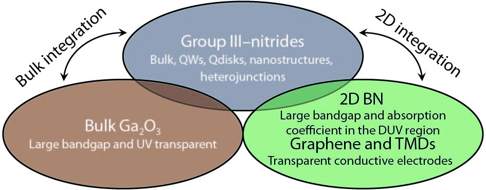


Set citation alerts for the article
Please enter your email address

© Copyright 2018-2021 | Chinese Laser Press. All Rights Reserved 沪ICP备15018463号-20