
Xiaorong Luo, Ke Zhang, Xu Song, Jian Fang, Fei Yang, Bo Zhang. 4H-SiC trench MOSFET with an integrated Schottky barrier diode and L-shaped P+ shielding region[J]. Journal of Semiconductors, 2020, 41(10): 102801
- Journal of Semiconductors
- Vol. 41, Issue 10, 102801 (2020)
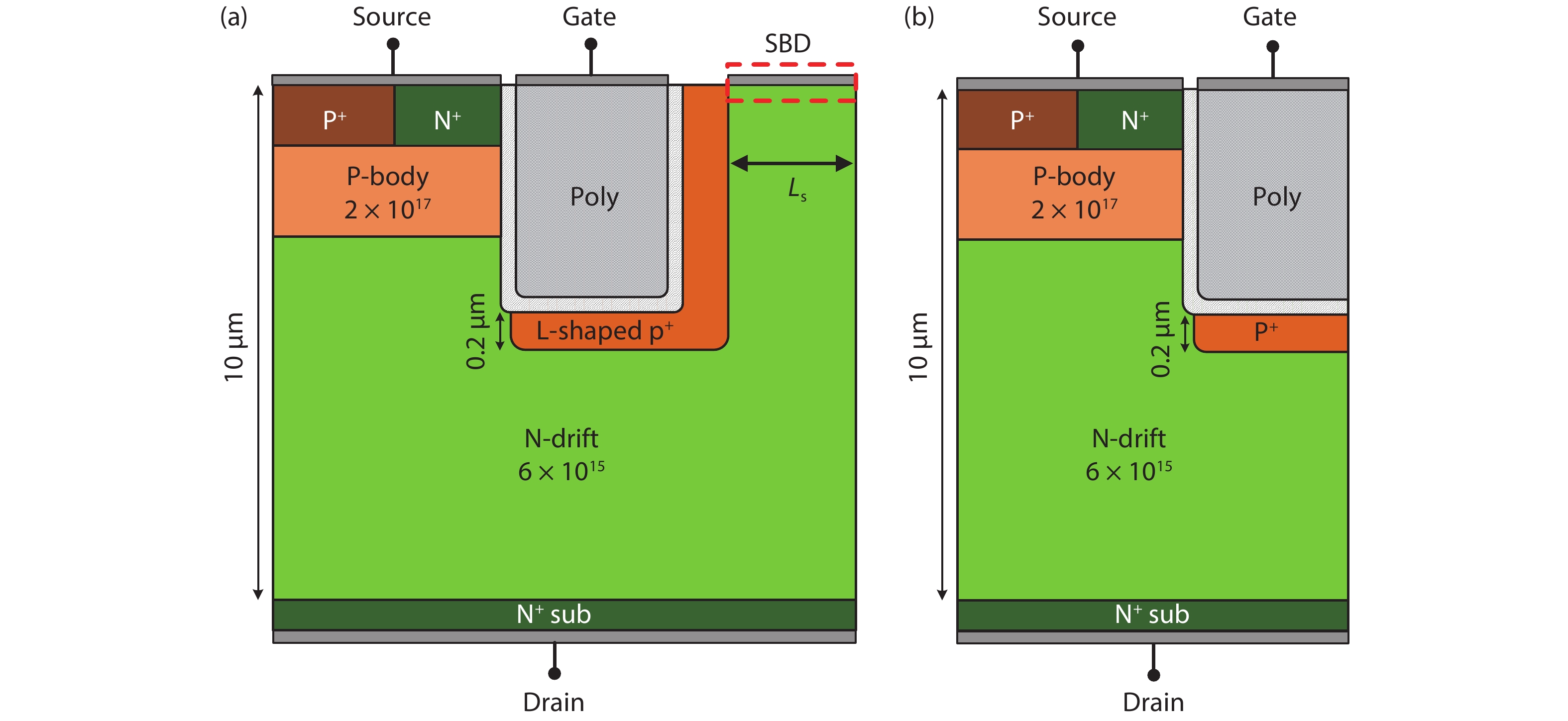
Fig. 1. (Color online) Device structure of (a) S-TMOS and (b) C-TMOS.
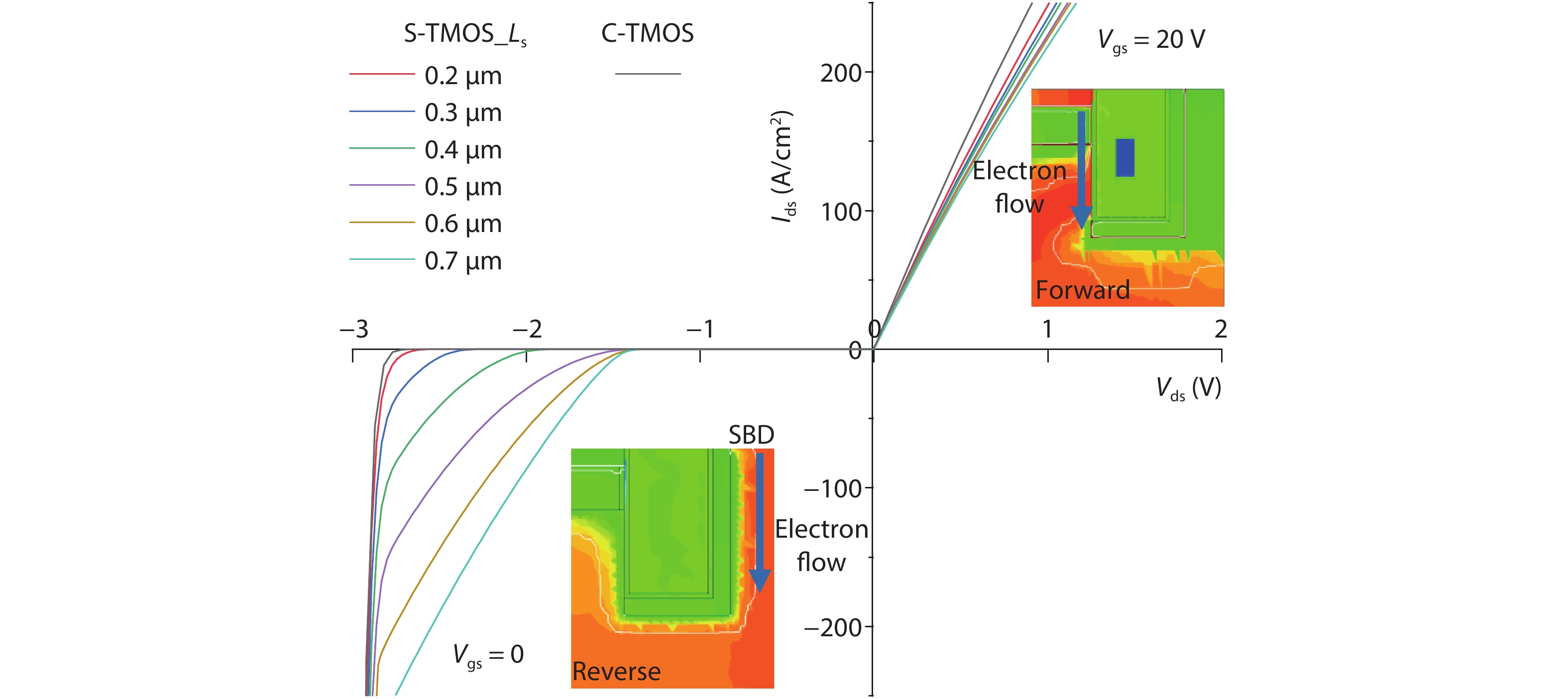
Fig. 2. (Color online) Forward and reverse conduction I–V characteristics of C-TMOS and S-TMOS with varied L s. The insets show the forward and reverse current contours of S-TMOS at V ds = +/– 2 V.
Fig. 3. (Color online) Test circuit for (a) S-TMOS, (b) C-TMOS, and (c) C-TMOS paralleled with an external SBD.
Fig. 4. (Color online) Reverse recovery current waveforms of C-TMOS, S-TMOS with varied L s and C-TMOS/SBD solution.
Fig. 5. (Color online) (a) Influence of L s on BV and Q rr of S-TMOS. (b) Leakage current of S-TMOS (L s = 0.5 µ m) and C-TMOS.
Fig. 6. (Color online) (a) Gate-Drain capacitance (C gd) of the C-TMOS and S-TMOS. (b) Gate charge characteristic curves of C-TMOS and S-TMOS.
Fig. 7. (Color online) (a) Test circuit for switching characteristic. (b) Turn- off waveforms of C-TMOS and S-TMOS.
Fig. 8. (Color online) (a) Dependence of switching loss (E on + E off) on gate resister R G. (b) Comparison of power losses as a function of switching frequency f (@ R G = 10 Ω).
Fig. 9. (Color online) Key fabrication process flows for the S-TMOS: (a) ion implantation to form the P-well and N+, P+ sources, (b) gate trench etching, (c) P+ shielding region implantation, (d) thermal oxidation to form the gate oxide, (e) poly silicon deposition, (f) metallization.
|
Table 1. Performance comparison of C-TMOS and S-TMOS.


Set citation alerts for the article
Please enter your email address

© Copyright 2018-2021 | Chinese Laser Press. All Rights Reserved 沪ICP备15018463号-20