
Xiaorong Luo, Ke Zhang, Xu Song, Jian Fang, Fei Yang, Bo Zhang. 4H-SiC trench MOSFET with an integrated Schottky barrier diode and L-shaped P+ shielding region[J]. Journal of Semiconductors, 2020, 41(10): 102801
- Journal of Semiconductors
- Vol. 41, Issue 10, 102801 (2020)
Abstract
1. Introduction
SiC MOSFET, as one of the most promising power switch devices, has replaced part of Si counterpart in many applications. In a common bridge rectifier circuit, SiC MOSFET is usually anti-paralleled with an external SiC Schottky barrier diode (SBD) as a free-wheeling diode (FWD), due to the bipolar degradation of the intrinsic body diode[
In this paper, we propose a novel SiC trench MOSFET with an integrated SBD and L-shaped P+ shielding region (S-TMOS). This device achieves excellent third quadrant performance with low Cgd and Qgd values. Moreover, the static and dynamic characteristics of the S-TMOS and conventional SiC trench MOSFET (C-TMOS) are compared in detail.
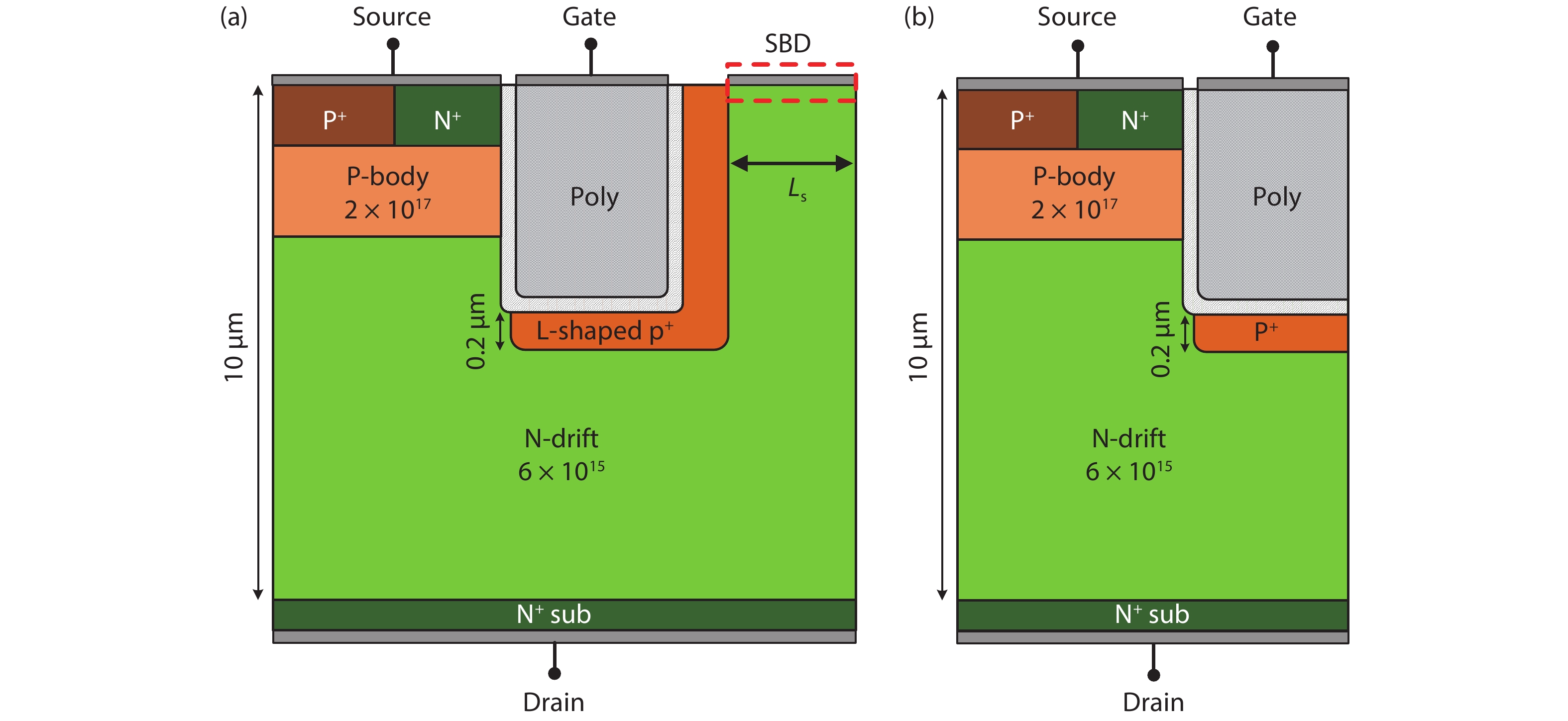
2. Device structure and mechanism
Schematic cross sections of the S-TMOS and C-TMOS are presented in Fig. 1. The main parameters of the two structures are given. Since the Schottky contact occupies a part of cell area, an excessive Ls leads to a large area and Ron,sp. Moreover, if Ls is too large, then the protection effect of the P+ shielding region on Schottky contact will be weakened and thus the leakage current may increase. In contrast, if Ls is too small, then the reverse conduction and reverse recovery performances of S-TMOS will degrade. The grounded P+ shielding region exists both beneath the gate trench and aside one side wall of the gate trench in S-TMOS. The S-TMOS has lower Cgd and Qgd than C-TMOS because the L-shaped P+ region shields the coupling of gate and drain more effectively. Meanwhile, the SBD is located next to the P+ shielding region so that the highly doped P+ region can absorb electric field lines from drain and reduce the surface electric field of the Schottky contact. The static and dynamic characteristics of S-TMOS and C-TMOS have been investigated by numerical TCAD simulations. The thickness of gate oxide is 50 nm and the channel mobility is set to be 20 cm2/(V·s). In order to form a favorable Schottky contact, nickel (Ni) is selected as the Schottky metal. The workfunction of Ni is between 5.04 and 5.35 eV[
![]()
Figure 1.(Color online) Device structure of (a) S-TMOS and (b) C-TMOS.
3. Results and discussion
Fig. 2 shows the static I–V characteristics of the S-TMOS with varied Ls and the C-TMOS. In reverse conduction condition, S-TMOS turns on earlier than C-TMOS because the integrated SBD turns on prior to the P-body/N-drift junction in C-TMOS. Moreover, the larger Ls is, the lower turn-on voltage is. This happens because the ratio of Schottky junction to PN junction is increased. When Vds is –2 V at Ls ≥ 0.4 µm, the SBD of S-TMOS has already turned on and the reverse current flows through the Schottky contact. While the intrinsic body diode of the C-TMOS has not turned on yet. When Ls > 0.5 µm, the VF of S-TMOS hardly drops anymore and remains at about 1.5 V, which is much lower than 2.7 V of C-TMOS. In forward conduction condition, all current in S-TMOS flows through the reverse layer channel, and the SBD does not work. The forward conduction characteristics of the two designs are similar. The different cell areas caused by different Ls make the Ron,sp of the devices slightly different. The Ron,sp of S-TMOS with Ls = 0.5 µm (4.44 mΩ·cm2) is a little bit larger than that of C-TMOS (3.71 mΩ·cm2).
![]()
Figure 2.(Color online) Forward and reverse conduction
The test circuits in Fig. 3 are used to evaluate the reverse recovery performance of the devices. VG is switched between 0 and +20 V. The chip areas of all devices are fixed to be 1 cm2. The load inductance and load current are 5 nH and 100 A/cm2, respectively.
![]()
Figure 3.(Color online) Test circuit for (a) S-TMOS, (b) C-TMOS, and (c) C-TMOS paralleled with an external SBD.
Fig. 4 shows the reverse recovery current waveforms of C-TMOS, S-TMOS with varied Ls and C-TMOS/SBD solution. The carriers stored in drift region must be fully extracted to withstand reverse voltage during reverse recovery, and this process will generate current overshoot. More carriers will cause larger current overshoot and prolonged oscillations. The current overshoot not only increases power consumption and slows down the transfer speed but also reduces reliability of the whole system. Since the reverse recovery current flows through the intrinsic body diode in C-TMOS and the intrinsic body diode is a bipolar device, C-TMOS has the largest current overshoot and Qrr. For S-TMOS, the reverse recovery current flows through the integrated SBD, resulting in better reverse recovery performance. As Ls increases, the reverse recovery current is lower and the reverse recovery time is shorter, so both the reverse recovery current oscillation and the Qrr decrease. Compared with C-TMOS paralleled with an external SBD, when Ls ≥ 0.5 µm, the S-TMOS achieves a lower forward current overshoot. Since the SBD integrated inside the cell of S-TMOS suppresses the bipolar conduction more effectively, the Qrr of S-TMOS (Ls = 0.5 µm) is only 1.25 µC, which is much smaller than that of C-TMOS (5.04 µC) and C-TMOS/SBD solution (2.11 µC).
![]()
Figure 4.(Color online) Reverse recovery current waveforms of C-TMOS, S-TMOS with varied
The influence of Ls on BV and Qrr of S-TMOS is shown in Fig. 5(a). With the increase in Ls, the reverse recovery performance of S-TMOS is greatly improved, resulting in a significantly reduced Qrr. The drain leakage current of C-TMOS and S-TMOS (Ls = 0.5 µm) at forward blocking state is shown in Fig. 5(b) and the distribution of equipotential lines is also shown in the inset. Since the P+ shielding region is deep enough, the protection effect on Schottky contact is very effectively. There is almost no potential line passing through the Schottky area and the electric field under high drain voltage is successfully shielded, thereby avoiding the barrier lowing of Schottky contact, so the breakdown voltage of S-TMOS is barely reduced compared with that of C-TMOS. Based on this discussion, the optimum value of Ls is selected as 0.5 µm and it is used in subsequent simulations.
![]()
Figure 5.(Color online) (a) Influence of
Gate–drain capacitance (Cgd) and gate–drain charge (Qgd) are key factors which affect the switching speed of power devices. Fig. 6(a) compares the Cgd of C-TMOS and S-TMOS under different drain-source voltages. The coupling effect between gate and drain is weakened due to the shielding effect of the L-shaped P+ region, resulting in reduced Cgd. The Cgd of C-TMOS and S-TMOS are 179 and 139 pF/cm2 at Vds = 600 V, respectively.
![]()
Figure 6.(Color online) (a) Gate-Drain capacitance (
Meanwhile, gate charges were tested with the circuit in the inset of Fig. 6(b). The load inductance and load current used in simulation are 10 nH and 100 A/cm2, respectively. The S-TMOS exhibits a narrower Miller platform and a lower Qgd value of 143 nC/cm2 than that of the C-TMOS (209 nC/cm2), as shown in Fig. 6(b). By the way, the rising slope of Vg for S-TMOS is a little bit lower before reaching Miller platform because the L-shaped P+ region shorted to source contact leads to a relatively larger gate-source charge Qgs. Therefore, S-TMOS has a desirable smaller ratio of Qgd relative to Qgs. This feature is crucial to suppress additional losses caused by a parasitic turn-on half bridge circuit and allows for a well-controlled switching with very low dynamic losses[
The simulation circuit for switching characteristic is presented in Fig. 7(a). The MOSFETs turn off at t = 25 μs and all device areas are 1 cm2. The load inductance used in simulation is 10 nH. A SiC Schottky barrier diode is used as the free-wheeling diode. The load current (IA) and the gate resistor (RG) are set as 100 A/cm2 and 10 Ω, respectively. Fig. 7(b) shows the turn-off waveforms of the two MOSFETs. The S-TMOS has a delay before turn-off process due to a larger Qgs, but there is almost no extra power consumption during the delay. Actually, the two devices have almost the same current rise time during turning on and fall time during turning off. Owning to a smaller Qgd, the S-TMOS achieves lower turn-off loss (Eoff) since Qgd plays a more important role in turning off. The Eoff of S-TMOS is 2.49 mJ/cm2, which has reduced by 19% compared with 3.08 mJ/cm2 of the C-TMOS.
![]()
Figure 7.(Color online) (a) Test circuit for switching characteristic. (b) Turn- off waveforms of C-TMOS and S-TMOS.
Fig. 8(a) shows the influence of the gate resister RG on switching loss (Eon + Eoff) in one switching cycle. The S-TMOS exhibits a lower switching loss at all different RG values. As RG increases, the difference of the switching loss between the two MOSFETs increases. The total power losses Pt of the device consists of conduction loss and switching loss, and can be calculated by[
![]()
Figure 8.(Color online) (a) Dependence of switching loss (
where k is the duty cycle defined as the ratio of the interval in which the MOSFET conducts versus the total period, and f is the switching frequency. Fig. 8(b) shows the power losses as a function of f and the duty cycle is set as 0.5. With the increase in switching frequency, conduction loss is almost negligible and switching loss becomes the major part of power dissipation. The advantage of S-TMOS also increases with the increasing frequency. When operating at 200 kHz, the S-TMOS realizes 13% reduction in the power losses compared with the C-TMOS.
Table 1 summarizes the performance parameters for the two devices. Obviously, the S-TMOS obtains better comprehensive performances than C-TMOS.
A feasible fabrication procedure is shown in Fig. 9. Tilted implantation is adopted to form the L-shaped P+ shielding region. To form the Schottky contact and ohmic contact at the same time, Nickel (Ni) single ohmic/Schottky contact process scheme is chosen in metallization process[
![]()
Figure 9.(Color online) Key fabrication process flows for the S-TMOS: (a) ion implantation to form the P-well and N+, P+ sources, (b) gate trench etching, (c) P+ shielding region implantation, (d) thermal oxidation to form the gate oxide, (e) poly silicon deposition, (f) metallization.
4. Conclusion
A novel SiC trench MOSFET with an integrated SBD and L-shaped P+ shielding region is proposed in this paper. The integrated SBD works as a free-wheeling diode with a low reverse on-state voltage and reverse recovery charge. Compared with conventional SiC trench MOSFET, the VF and Qrr of S-TMOS has reduced by 44% and 75% without sacrificing the BV, resulting in excellent third quadrant characteristic. Furthermore, the P+ shielding region reduces the gate–drain capacitance and gate–drain charge. The Qgd and Cgd of S-TMOS reduce by 32% and 22% in comparison with that of C-TMOS, leading to lower switching power consumption. Furthermore, due to the P+ shielding region, the leakage current hardly increases with the increase of drain-source voltage. The S-TMOS is much more competitive and promising in high power and high frequency applications.
Acknowledgements
This work was supported by the National Key Research and Development Program of China (No. 2016YFB0400502).
References
[1]
[2]
[3]
[4] X Li, X Tong, A Q Huang et al. SiC trench MOSFET with integrated self-assembled three-level protection Schottky barrier diode. IEEE Trans Electron Devices, 65, 347(2017).
[5] Y Kobayashi, H Ishimori, A Kinoshita et al. Evaluation of Schottky barrier height on 4H-SiC m-face {1
[6] Q He, X Luo, T Liao et al. 4H-SiC superjunction trench MOSFET with reduced saturation current. Superlattices Microstruct, 125, 58(2019).
[7] X R Luo, T Liao, J Wei et al. A novel 4H-SiC trench MOSFET with double shielding structures and ultralow gate-drain charge. J Semicond, 40, 052803(2019).
[8] M Zhang, J Wei, H Jiang et al. A new SiC trench MOSFET structure with protruded p-base for low oxide field and enhanced switching performance. IEEE Trans Device Mater Reliab, 17, 432(2017).
[9] K Han, B J Baliga, W Sung. A novel 1.2 kV 4H-SiC buffered-gate (BG) MOSFET: Analysis and experimental results. IEEE Electron Device Lett, 39, 248(2017).
[10]
[11] H Jiang, J Wei, X Dai et al. SiC trench MOSFET with shielded fin-shaped gate to reduce oxide field and switching loss. IEEE Electron Device Lett, 37, 1324(2016).
[12]
[13]
[14]
[15] J Lutz, H Schlangenotto, U Scheuermann et al. Semiconductor power devices: Physics, characteristics, reliability. Electron Power, 24, 599(2011).
[16] X Zhou, R Yue, J Zhang et al. 4H-SiC trench MOSFET with floating/grounded junction barrier-controlled gate structure. IEEE Trans Electron Devices, 64, 4568(2017).
[17] W Sung, a B J Baliga. Monolithically integrated 4H-SiC MOSFET and JBS diode (JBSFET) using a single ohmic/Schottky process scheme. IEEE Electron Device Lett, 37, 1605(2016).
[18] W Sung, a B J Baliga. On developing one-chip integration of 1.2 kV SiC MOSFET and JBS diode (JBSFET). IEEE Trans Ind Electrons, 64, 8206(2017).

Set citation alerts for the article
Please enter your email address
© Copyright 2018-2021 | Chinese Laser Press. All Rights Reserved 沪ICP备15018463号-20