
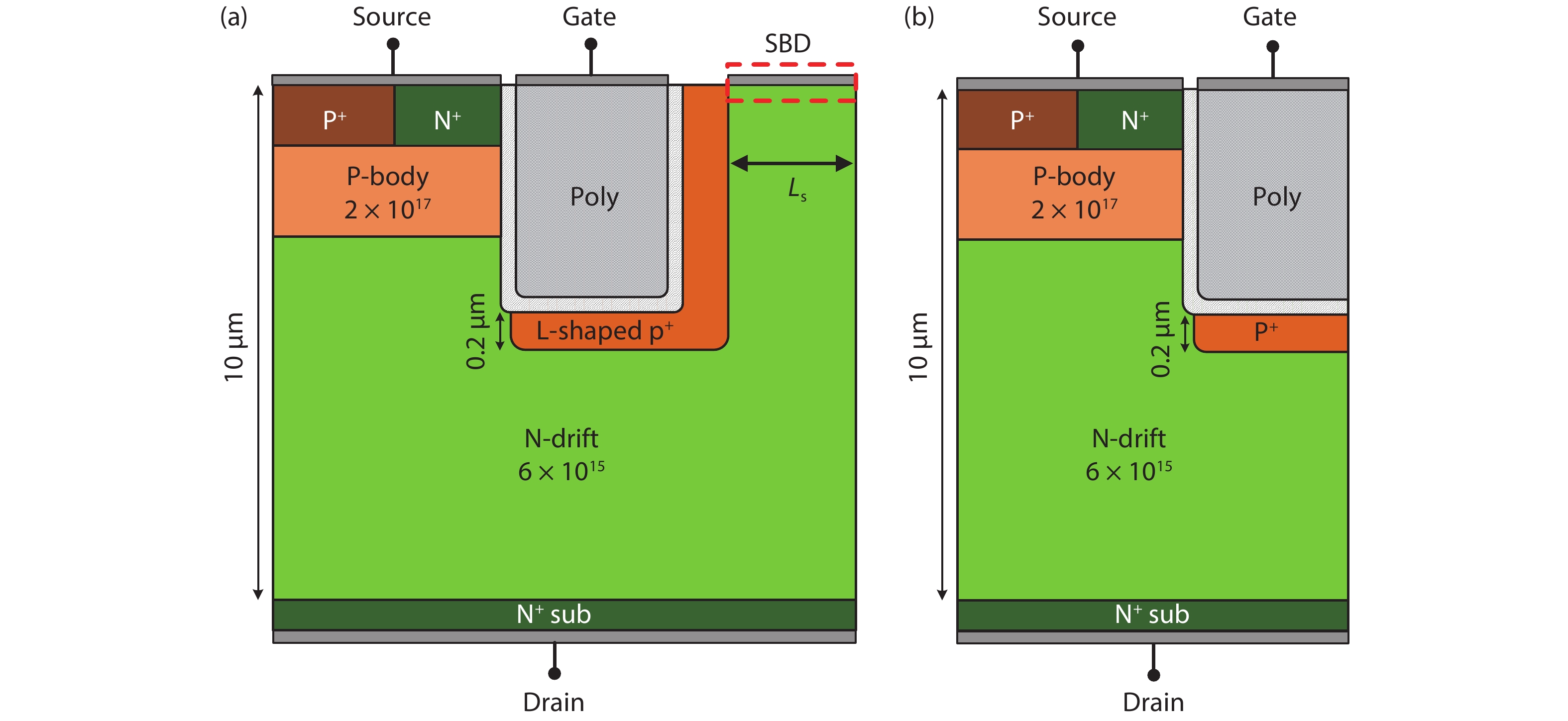
Xiaorong Luo, Ke Zhang, Xu Song, Jian Fang, Fei Yang, Bo Zhang. 4H-SiC trench MOSFET with an integrated Schottky barrier diode and L-shaped P+ shielding region[J]. Journal of Semiconductors, 2020, 41(10): 102801
- Journal of Semiconductors
- Vol. 41, Issue 10, 102801 (2020)
Abstract
| () |
View in Article


Set citation alerts for the article
Please enter your email address

© Copyright 2018-2021 | Chinese Laser Press. All Rights Reserved 沪ICP备15018463号-20