• Journal of Semiconductors
  • Vol. 40, Issue 12, 122402 (2019)
Zhangli Liu, Bingkui He, Fei Meng, Qiang Bao, Yuhong Sun, Shaojun Sun, Guangwei Zhou, Xiuliang Cao, and Haiwei Xin
Author Affiliations
  • Shanghai Huahong Grace Semiconductor Manufacturing Corporation, Shanghai 201203, China
  • show less
    DOI: 10.1088/1674-4926/40/12/122402 Cite this Article
    Zhangli Liu, Bingkui He, Fei Meng, Qiang Bao, Yuhong Sun, Shaojun Sun, Guangwei Zhou, Xiuliang Cao, Haiwei Xin. Contact etch process optimization for RF process wafer edge yield improvement[J]. Journal of Semiconductors, 2019, 40(12): 122402 Copy Citation Text show less
    (Color online) Yield loss map induced by the CT open issue.
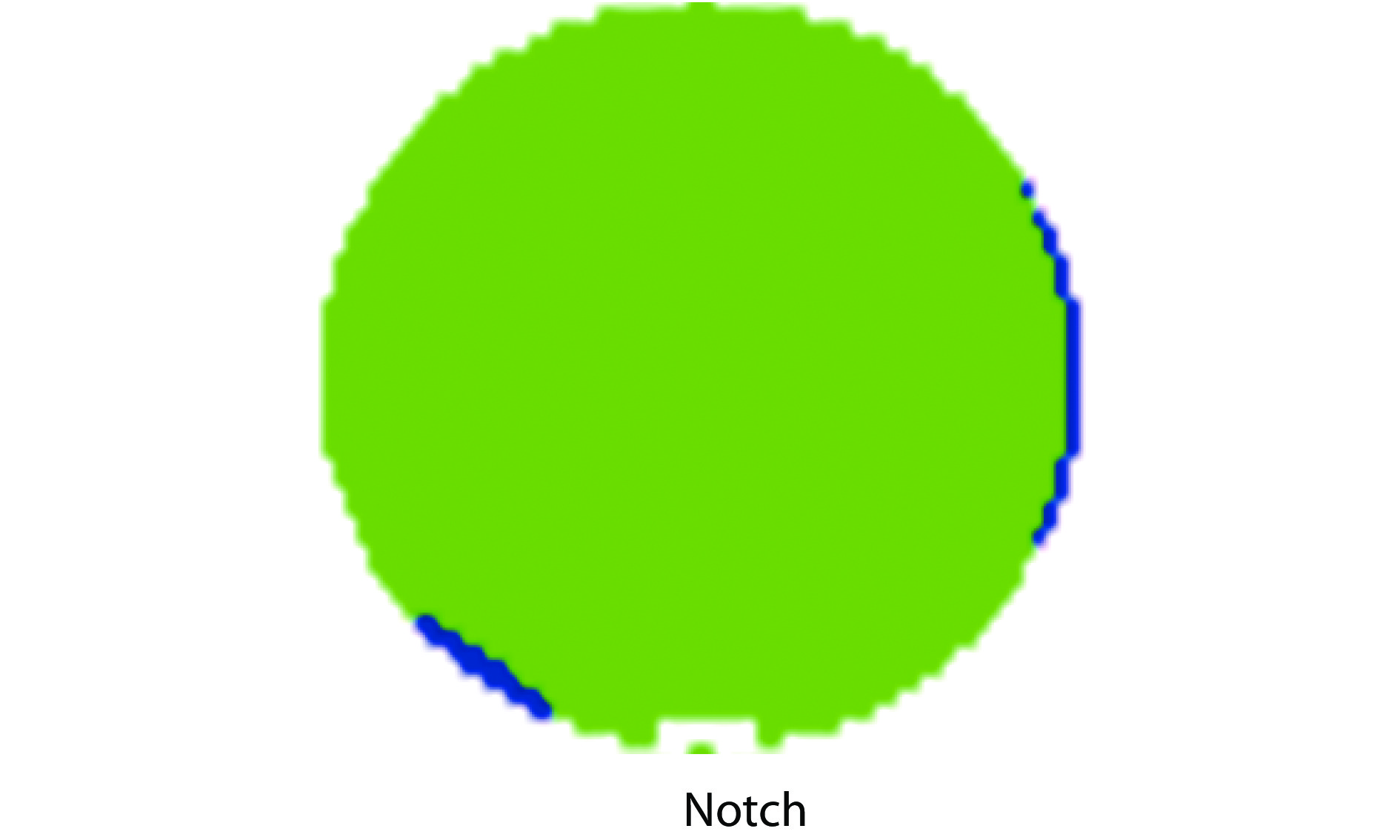
    Fig. 1. (Color online) Yield loss map induced by the CT open issue.
    FA SEM result for a CP fail sample at different pattern regions: (a) CT on poly-sparse pattern; (b) CT on an active region; and (c) CT on a poly-dense pattern. M1 is metal 1 for electrical connection, ILD is inter-layer-dielectric, ACT is active region for device, poly is for MOSFET or resistance, salicide is formed between CT and ACT/poly.
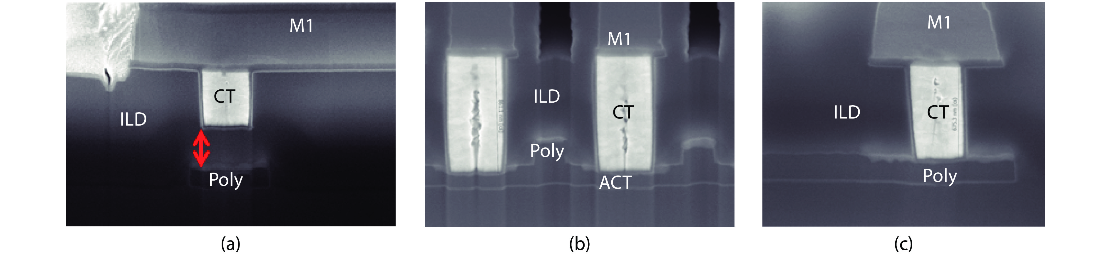
    Fig. 2. FA SEM result for a CP fail sample at different pattern regions: (a) CT on poly-sparse pattern; (b) CT on an active region; and (c) CT on a poly-dense pattern. M1 is metal 1 for electrical connection, ILD is inter-layer-dielectric, ACT is active region for device, poly is for MOSFET or resistance, salicide is formed between CT and ACT/poly.
    Failure mechanism for CT open for sparse poly-pattern at most of the wafer’s edge. (a) CT pattern top view. (b) BARC layer wafer center. (c) CT formed at wafer center. (d) BARC layer wafer edge. (e) CT formed at wafer edge.
    Fig. 3. Failure mechanism for CT open for sparse poly-pattern at most of the wafer’s edge. (a) CT pattern top view. (b) BARC layer wafer center. (c) CT formed at wafer center. (d) BARC layer wafer edge. (e) CT formed at wafer edge.
    (Color online) Instruction for CT etch BT and ME steps pre- and post-optimization. The blue line is normal CT etch process for wafer center; the red line is pre-optimization CT etch process at wafer edge; the green line is post-optimization CT etch process at wafer edge.
    Fig. 4. (Color online) Instruction for CT etch BT and ME steps pre- and post-optimization. The blue line is normal CT etch process for wafer center; the red line is pre-optimization CT etch process at wafer edge; the green line is post-optimization CT etch process at wafer edge.
    (Color online) (a) Yield map and (b) SEM result at CT on sparse poly-pattern at wafer edge with CT etch optimization recipe.
    Fig. 5. (Color online) (a) Yield map and (b) SEM result at CT on sparse poly-pattern at wafer edge with CT etch optimization recipe.
    TEM result for CT etch process with (a) POR and (b) post-optimization recipe.
    Fig. 6. TEM result for CT etch process with (a) POR and (b) post-optimization recipe.
    (Color online) RcN+ and RcP+ WAT mapping data BOX chart. W.26 mean the CT size is 0.26 × 0.26 µm2.
    Fig. 7. (Color online) RcN+ and RcP+ WAT mapping data BOX chart. W.26 mean the CT size is 0.26 × 0.26 µm2.
    CT etch stepBARCILD oxide
    1st stepBT (CF4 base)12.938
    2nd stepME (C5F8 base)0.1021
    Table 1. Etch rate for BARC and ILD oxide.
    Zhangli Liu, Bingkui He, Fei Meng, Qiang Bao, Yuhong Sun, Shaojun Sun, Guangwei Zhou, Xiuliang Cao, Haiwei Xin. Contact etch process optimization for RF process wafer edge yield improvement[J]. Journal of Semiconductors, 2019, 40(12): 122402
    Download Citation