
Zhangli Liu, Bingkui He, Fei Meng, Qiang Bao, Yuhong Sun, Shaojun Sun, Guangwei Zhou, Xiuliang Cao, Haiwei Xin. Contact etch process optimization for RF process wafer edge yield improvement[J]. Journal of Semiconductors, 2019, 40(12): 122402
- Journal of Semiconductors
- Vol. 40, Issue 12, 122402 (2019)
Abstract
1. Introduction
CMOS technology has emerged as the leading solution due to its cost advantage, performance improvement, and ease of integration for high-performance digital circuits and high-speed analog/RF circuits. Recently, the CMOS compatible RF process has become the mainstream solution for RF front end modules, especially for switch applications[
2. Experiment result and discussion
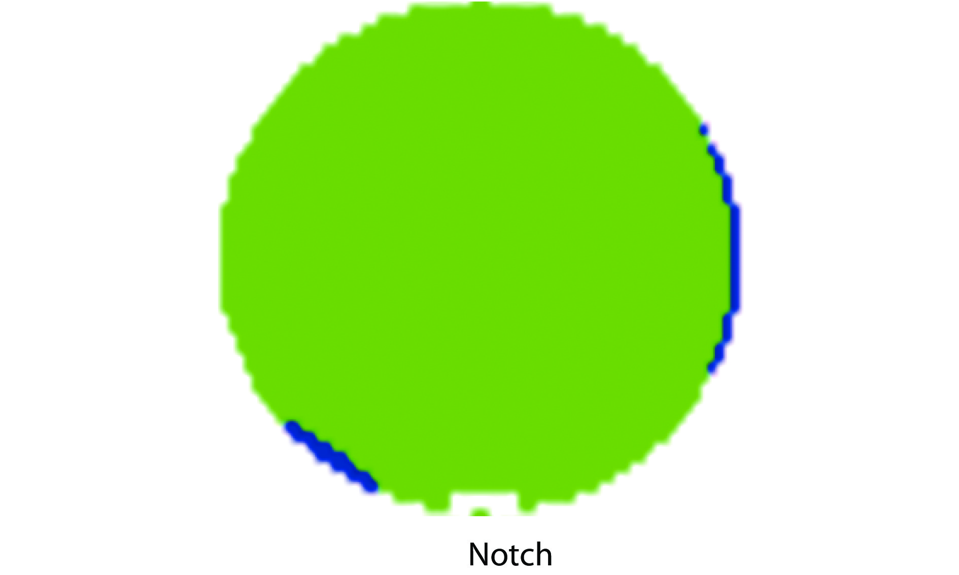
As shown in Fig. 1, some RF process products suffer from wafer edge yield loss. The yield loss is observed at 3 o’clock and 7 o’clock at the wafer’s edge. The notch is located on the bottom of the wafer. According to the definition of a failure bin, the yield loss is induced by circuit OPEN. As shown in Fig. 2, contact (CT) open is observed for a poly-sparse pattern at the wafer’s edge by scanning electron microscope (SEM). However, no abnormality is observed for the poly-dense pattern and active region. For the RF process platform, an active region (ACT) is generally used for active devices, such as MOSFETs and diodes. The poly-major is located at the top of shallow trench isolation (STI) region, such as the high resistivity resistance, which is used for DC bias control terminal. To reduce the coupling and parasitic effect, ACT and poly-dummy patterns are forbidden. Consequently, an obvious distinction is observed for different poly-pattern regions.
![]()
Figure 1.(Color online) Yield loss map induced by the CT open issue.
![]()
Figure 2.FA SEM result for a CP fail sample at different pattern regions: (a) CT on poly-sparse pattern; (b) CT on an active region; and (c) CT on a poly-dense pattern. M1 is metal 1 for electrical connection, ILD is inter-layer-dielectric, ACT is active region for device, poly is for MOSFET or resistance, salicide is formed between CT and ACT/poly.
In the device manufacturing process, edge bead removal (EBR) is carried out during the PH loop by directing a controlled stream of developer solvent at the edge of the wafer. Wafer edge exposure (WEE) is often used together with EBR. A clean ring is created at the wafer’s edge[
ILD can be introduced by plasma-enhanced chemical vapor deposition (PECVD) SiN, boro-phospho-silicate-glass (BPSG) deposition and densify post the front-end-of-line (FEOL) CMOS process[
![]()
Figure 3.Failure mechanism for CT open for sparse poly-pattern at most of the wafer’s edge. (a) CT pattern top view. (b) BARC layer wafer center. (c) CT formed at wafer center. (d) BARC layer wafer edge. (e) CT formed at wafer edge.
The aim is to optimize the CT etch process. The etch process has previously been studied[
Based on the FA SEM result, the ILD thickness is thinner for the poly-sparse pattern at the wafer’s edge. During the BARC layer process loop, a thicker BARC layer is formed at the poly-sparse pattern at most of the wafer’s edge region. The thickness of BARC and ILD under the etching process is shown in Fig. 4. The blue marked line is the instruction for CT etch process with normal BARC thickness. The CT etch first step is BT with CF4 base, this step etch oxide is also relatively high. However, the second ME step with C5F8 base, the etch rate for BARC layer is relatively lower. Suppose that the BARC layer is thicker at the sparse poly-pattern at most of the wafer’s edge (TBARC_E > TBARC_C). When the BT step is not enough for the BARC layer etch, the ME step will consume most of the time to open the BARC due to the low etch rate. As shown in Fig. 4, the red line marked ILD oxide is not fully etched. Consequently, the height post CT etch is relatively lower, and cannot even touch the top salicide of the sparse poly-pattern. CT open is observed, which leads to circuit OPEN and yield loss. By increasing the tBT to tBT’, there is no BARC residue post-BT etch, the ME can then etch the ILD oxide smoothly. In other words, by increasing the BT time to make sure that there is enough BARC layer etch, we can avoid the CT open issue.
![]()
Figure 4.(Color online) Instruction for CT etch BT and ME steps pre- and post-optimization. The blue line is normal CT etch process for wafer center; the red line is pre-optimization CT etch process at wafer edge; the green line is post-optimization CT etch process at wafer edge.
Based on the proposed failure mechanism and etch rate, an experiment that increases the BT time is applied. By increasing 50% BT time, CT open is avoided at the poly-sparse pattern at most of the wafer’s edge. The optimization result is shown in Fig. 5. The CP yield map is normal for the optimization CT etch recipe. During the recipe optimization, we keep the ME time because the etch rate of C5F8 on BARC is too low. Based on the SEM result for CT on sparse poly-pattern and CP data, increasing the BT time is efficient. The SEM result for CT on ACT and dense poly is not shown for the sake of clarity.
![]()
Figure 5.(Color online) (a) Yield map and (b) SEM result at CT on sparse poly-pattern at wafer edge with CT etch optimization recipe.
As shown in the Fig. 6 (TEM picture), the CT tungsten touched the poly-salicide well. The salicide thickness is comparable with the baseline center one. During the CT etch process, the etch loop will stop on the salicide layer. The increased BT time may induce salicide damage. The CT profile is checked by TEM for sparse poly-pattern located at the wafer’s center. As shown in Fig. 6, no abnormality is observed for the CT/salicide/poly profile with the optimization etch recipe. The thickness of the salicide is comparable for POR and for the post-optimization recipe. N plus (RcN+) and P Plus (RcP+) type contact resistance is monitored after the full process loop. As shown in Fig. 7, the resistance mapping test result for RcN+ and RcP+ is comparable for POR and the optimization CT etch recipe. The 54 testkey sites on the wafer are summarized in a BOX chart. The uniformity is a little better for the post-optimization version.
![]()
Figure 6.TEM result for CT etch process with (a) POR and (b) post-optimization recipe.
![]()
Figure 7.(Color online) RcN+ and RcP+ WAT mapping data BOX chart. W.26 mean the CT size is 0.26 × 0.26
3. Conclusion
In summary, RF process wafer edge yield improvement is obtained by CT etch recipe optimization. A failure mechanism is proposed based on the wafer edge film stack characteristics. The large step height at wafer’s edge leads to worse planarization for the sparse poly-pattern region during the ILD CMP process. A thicker BARC layer is introduced for sparse poly-pattern at the wafer’s edge region. The contact open issue is solved by increasing the BT time to get enough window. A good SEM result for CT on sparse poly-pattern and improved CP data are obtained with an optimized etch recipe. A good profile for CT/salicide/poly at the wafer’s center is obtained by TEM. Finally, good uniformity is observed for the RcN+ and RcP+ resistance by the mapping test.
Acknowledgments
This work was supported by Shanghai Rising-Star Program (B type) (No. 18QB1401900).
References
[1] B K Esfeh, M Rack, K B Ali et al. RF small- and large-signal characteristics of CPW and TFMS lines on trap-rich HR-SOI substrates. IEEE Trans Electron Devices, 65, 3120(2018).
[2] M Jaffe, M Abou-Khalil, A Botula et al. Improvements in SOI technology for RF switches. IEEE 15th Topical Meeting on Silicon Monolithic Integrated Circuits in RF Systems, 30(2015).
[3] F Gianesello, A Monroy, V Vialla et al. Highly linear and sub 120 fs
[4] C Maleville, G Celler. SOI: Challenges and solutions to increasing yield in an ultrathin age. Yield Management Solutions, 6(2004).
[5] B Delahaye, J L Baltzinger, L Denis et al. Edge and extreme edge wafer manufacturing on 200 mm wafer: methodology, yield challenges, cost effective solutions, limitations. IEEE/SEMI Advanced Semiconductor Manufacturing Conference, 100(2009).
[6] I A N Goh, H S Chua, T L Neo et al. An integrated engineering approach to improve wafer edge yield. IEEE International Symposium on Semiconductor Manufacturing Conference Proceedings, 351(2001).
[7] K R Harris, B Y Ang. Yield implications of wafer edge engineering. International Symposium on Microelectronics & Assembly, 70(2000).
[8]
[9]
[10] Y W Men, H Zhang, K Zhou et al. Wafer back pressure control and optimization in the CMP process. J Semicond, 32, 126002(2011).
[11] J W Zhou, Y L Liu, W Zhang. Study of CMP lapping technique of ULSI silicon substrate. J Semicond, 28, 572(2007).
[12] M Boumerzoug. Optimized BARC films and etch byproduct removal for wafer edge defectivity reduction. 25th Annual SEMI Advanced Semiconductor Manufacturing Conference, 330(2014).
[13] H S Hu, M Zhang. Modeling for charging effect during RIE processing. Chin J Electron, 28, 81(2000).
[14] H T Ding, Z C Yang, G Z Yan. A dual-purpose method to enhance heat transfer and prevent notching effect in deep reactive ion etching. Chin J Electron, 38, 1201(2010).


Set citation alerts for the article
Please enter your email address

© Copyright 2018-2021 | Chinese Laser Press. All Rights Reserved 沪ICP备15018463号-20