
Xinyu Wu, Weihua Han, Xiaosong Zhao, Yangyan Guo, Xiaodi Zhang, Fuhua Yang. Gate-regulated transition temperatures for electron hopping behaviours in silicon junctionless nanowire transistors[J]. Journal of Semiconductors, 2020, 41(7): 072905
- Journal of Semiconductors
- Vol. 41, Issue 7, 072905 (2020)
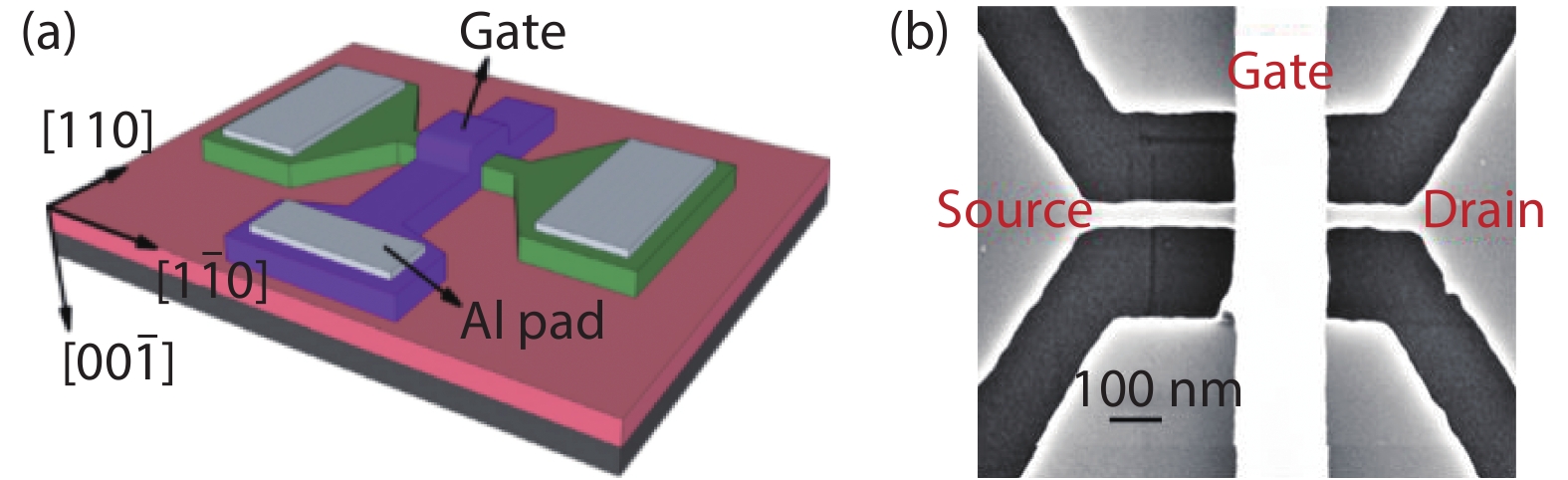
Fig. 1. (Color online) (a) Schematic structure of the silicon JNT. (b) Top-view SEM images of the silicon JNT after gate formation.
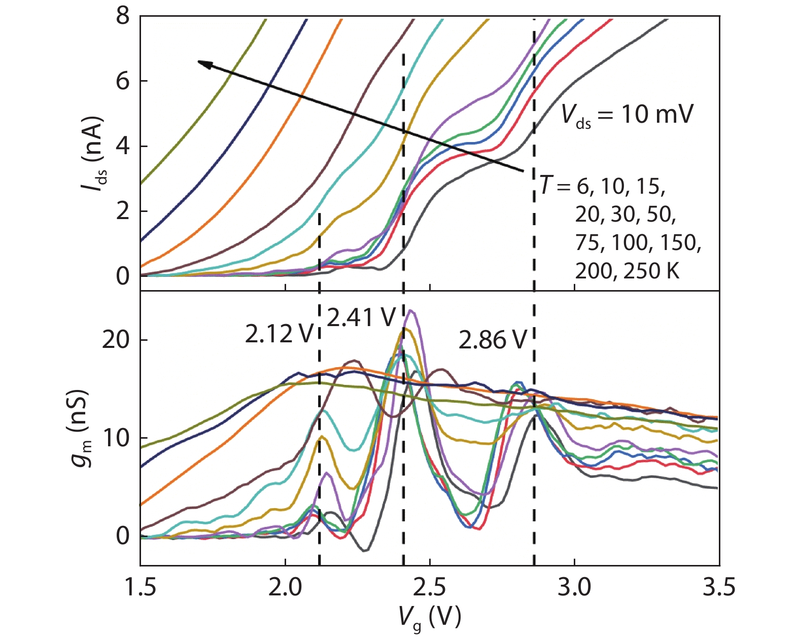
Fig. 2. (Color online) Drain current I ds versus gate voltage V g with V ds = 10 mV at different temperatures (upper part) and corresponding transconductance g m–V g curves (lower part).
Fig. 3. (Color online) (a) Barrier height of the device channel is extracted by fitting the thermally activated current. The conduction band edge E C reaches the Fermi level E F at 2.40 V. Inset: transconductance g m–V g curves at low temperature. (b) Locally amplified transconductance g m–V g curves before gate voltage 2.40 V, which are successively shifted for clarify.
Fig. 4. (Color online) Arrhenius plots of the conductance G 1, G 2, G 3, and G 4 for each group. The inset: close-up of the curves around 75 K.
Fig. 5. (Color online) (a) The gate-voltage regulated transition temperature T A and T C. (b) The gate-voltage dependence of the density of state and the localization length.
Fig. 6. (Color online) The behaviour of electron hopping (a) from M-VRH to NNH in and (b) from ES-VRH to M-VRH in.

Set citation alerts for the article
Please enter your email address
© Copyright 2018-2021 | Chinese Laser Press. All Rights Reserved 沪ICP备15018463号-20