
Xinyu Wu, Weihua Han, Xiaosong Zhao, Yangyan Guo, Xiaodi Zhang, Fuhua Yang. Gate-regulated transition temperatures for electron hopping behaviours in silicon junctionless nanowire transistors[J]. Journal of Semiconductors, 2020, 41(7): 072905
- Journal of Semiconductors
- Vol. 41, Issue 7, 072905 (2020)
Abstract
1. Introduction
Dopant atoms may draw more attention when they are used as a functional unit of ultra-small electronic devices instead of just providing carriers[
Electron transport in the discrete dopant atomic system may be dominated by thermally assisted hopping between the dopants rather than by resonant tunnelling between source and drain. At higher temperatures, electrons can hop between the neighbouring dopants when they receive enough energy from a phonon, following the nearest-neighbour hopping (NNH) mechanism. The conductance in this case is given by
The conductive channel in silicon junctionless nanowire transistor expands from the middle of the nanowire to the surrounding by adjusting the gate voltage. Once the junctionless nanowire transistor is turned on, the channel of electron transport can be seen as a quasi three-dimensional (3D) system. In the 3D case, the conductance follows the Mott law (M-VRH)[
where
where
2. Device fabrication and characterization
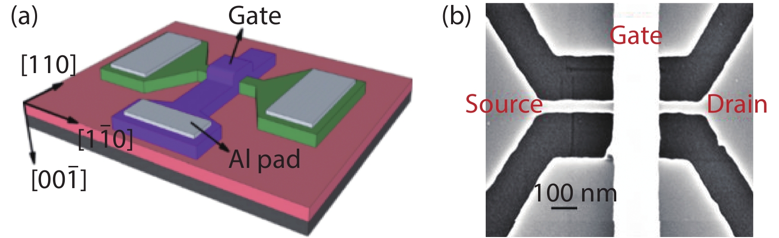
Fig. 1(a) shows a schematic of the devices fabricated on a (100)-oriented silicon-on-insulator (SOI) wafer with top silicon thickness of 55 nm and buried oxide layer of 145 nm. The SOI wafer with a 17-nm thermal oxidation layer was uniformly implanted by 33 keV phosphorus ions at a dose of 2 × 1012 cm–2, followed by rapid annealing to activate dopant atoms. The silicon nanowire was defined by electron beam lithography (EBL) and reactive ion etching (RIE), followed by thermal oxidation at 900 °C to form a sacrificial oxidation layer. Next, this sacrificial oxidation layer was removed by buffered oxide etcher (BOE) to smooth the surface and further reduce the dimension of silicon nanowire. After formation of 22-nm-thick gate oxidation layer around the nanowire at 900 °C in dry oxygen, 200-nm-thick boron-doped polycrystalline silicon was deposited on the devices by low-pressure chemical vapor deposition (LPCVD). Subsequently, the polycrystalline silicon gate of 280 nm was patterned by electron beam lithography and dry etching, followed by deposition of 200 nm SiO2 for passivation and fabrication of the source, drain and gate electrodes. The width of 60 nm for Si/SiO2 core-shell nanowire measured by scanning electron microscope (SEM) is shown in Fig. 1(b). According to the consumption of top silicon layer by thermal oxidation in all directions, the cross-section of the silicon core is estimated to be 16 × 28 nm2. The electrical characteristics were measured by Agilent B1500 semiconductor parameter analyzer, and the devices were placed in a vacuum chamber which can be cooled down to 6 K with the help of a Lakershore-340 temperature controller.
![]()
Figure 1.(Color online) (a) Schematic structure of the silicon JNT. (b) Top-view SEM images of the silicon JNT after gate formation.
3. Results and discussion
Fig. 2 shows drain current–gate voltage (Ids–Vg) characteristics (upper part) and corresponding transconductance gm–Vg characteristics (lower part) of JNT at the drain–source bias Vds = 10 mV by varying temperature. Clearly, a series of drain-current oscillatory peaks and steps are observed below the temperature of 75 K, and these current features gradually disappear with increasing temperature due to thermal energy broadening around Fermi level. The drain current at low temperature, which evolves from oscillatory peaks to current steps with the gate voltage, reflects that electron transport in dopant-levels gradually transfers into one-dimensional transport in conduction sub-bands. Similar features have also been observed in other devices that have been fabricated in the same way. According to the corresponding curves of the transconductance gm as a function of gate voltage Vg (i.e.,
![]()
Figure 2.(Color online) Drain current
To distinguish the three groups of transconductance peaks precisely, we measured the energy barrier between source and drain extracted from the thermally activated current at temperatures above 150 K. As shown in Fig. 3(a), the barrier height gradually decreases with gate voltage, which is associated with lower activation energy at larger electrical field. The gate voltage at 2.40 V can be determined by linear extrapolation of the curve to zero barrier height, showing that the conduction band edge Ec reaches the Fermi level EF of the source. It can be also observed that the position of gate voltage 2.40 V corresponds to a demarcation line between the first group of transconductance peaks and the other two groups in the inset of Fig. 3(a). As a result, the first group of transconductance peaks in Fig. 2 comes from discrete dopant-levels below the conduction edge. Then, one-dimensional transport of electrons occurs in the conduction sub-bands with the increase of gate voltage, resulting in the second and third groups of transconductance peaks.
![]()
Figure 3.(Color online) (a) Barrier height of the device channel is extracted by fitting the thermally activated current. The conduction band edge
We can identify new four groups of peaks marked by cross in Fig. 3(b) through locally amplifying the transconductance gm–Vg curves before 2.40 V. Since the gate-voltage spacing of those peaks is small and the positions of them are basically the same at different temperatures, those transconductance peaks can not originate from the surface roughness of the silicon nanowire. It is reported that dopants in the conductive channel have an effect on electron transport when the JNT is just turned on[
To obtain a better insight into the electron hopping mechanism, we experimentally extracted the conductance values at the position of transconductance peaks in each group, and those unrecognizable peaks at high temperatures are determined by the method of energy level alignment. Fig. 4 shows the Arrhenius plots (G versus 1/T) of temperature-dependent conductance G1, G2, G3, and G4, respectively at the transconductance peaks of different gate voltages under the bias Vds = 10 mV. Three regions (i.e., A, B, and C) in the Arrhenius plots of conductance correspond to NNH, M-VRH and ES-VRH. The transition temperature TA from NNH to M-VRH is a critical point at which the hopping distance in M-VRH is supposed to be equivalent to the mean distance between neighbouring dopant atoms. The expression of TA is given by
![]()
Figure 4.(Color online) Arrhenius plots of the conductance
The gate-voltage dependence of the transition temperatures is provided in the Fig. 5(a). It can be found that TA is relatively stable for the transconductance peak and valley positions, while TC increases with the increase of gate voltage. The difference between TA and TC is associated with the density of state g0 and the localization length, as shown in Fig. 5(b). According to the Eqs. (2) and (3), the characteristic temperatures TM and TES can be derived from the slopes of the
![]()
Figure 5.(Color online) (a) The gate-voltage regulated transition temperature
To understand the stable transition temperature TA at which electron hopping behaviours from M-VRH to NNH occurs, in Fig. 6(a) we describe the transition of hopping behaviours. Mott’s model has pointed out that electrons localized close to the Fermi level could hop from one localized site to another with the lowest activation energy
![]()
Figure 6.(Color online) The behaviour of electron hopping (a) from M-VRH to NNH in and (b) from ES-VRH to M-VRH in.
The gate-dependent transition temperature TC is regulated by the density of states and the localization length
4. Conclusion
In conclusion, we investigate gate-regulated transition temperatures of electron hopping behaviours in silicon junctionless nanowire transistor. The experimental data of temperature-dependent conductance illustrated by the Arrhenius plots is consistent with the theoretical model, showing that the electron hopping is ES-VRH, M-VRH and NNH with the increase of temperature. The transition temperature TA is relatively stable and mainly depends on the mean distance between the dopant atoms. In contrast, the transition temperature TC can be regulated by gate electrical field due to the longer localization length in the case of ES-VRH. The role of dopant atoms used as functional units becomes more and more important in ultra-small devices and the study on electron hopping by dopant atoms is of great significance to the development of those atomic-scale silicon transistors.
Acknowledgements
The authors acknowledge Dr. Hao Wang, Dr. Liuhong Ma and Mr. Xiaoming Li for their helps in device fabrication. This work was supported by the National Key R&D Program of China (Grant No.2016YFA0200503).
References
[1] P M Koenraad, M E Flatté. Single dopants in semiconductors. Nat Mater, 10, 91(2011).
[2] G P Lansbergen, R Rahman, C J Wellard et al. Gate-induced quantum-confinement transition of a single dopant atom in a silicon FinFET. Nat Phys, 4, 656(2008).
[3] B Fresch, J Bocquel, S Rogge et al. A probabilistic finite state logic machine realized experimentally on a single dopant atom. Nano Lett, 17, 1846(2017).
[4] L C L Hollenberg, A Dzurak, C J Wellard et al. Charged-based quantum computing using single donors in semiconductors. Phys Rev B, 69, 113301(2004).
[5] T D Ladd, F Jelezko, R Laflamme et al. Quantum computers. Nature, 464, 45(2010).
[6] M Fuechsle, J A Miwa, S Mahapatra et al. A single-atom transistor. Nat Nanotechnol, 7, 242(2012).
[7] E Prati, M Hori, F Guagliardo et al. Anderson–Mott transition in arrays of a few dopant atoms in a silicon transistor. Nat Nanotechnol, 7, 443(2012).
[8] S A Dagesyan, V V Shorokhov, D E Presnov et al. Sequential reduction of the silicon single-electron transistor structure to atomic scale. Nanotechnology, 28, 225304(2017).
[9] H Ryu, S Lee, M Fuechsle et al. A tight-binding study of single-atom transistors. Small, 3, 374(2015).
[10] M Tabe, D Moraru, M Ligowski et al. Single-electron transport through single dopants in a dopant-rich environment. Phys Rev Lett, 105, 016803(2010).
[11] Y Li, S Yu, J Hwang et al. discrete dopant fluctuations in 20-nm/15-nm-gate planar CMOS. IEEE Trans Electron Devices, 55, 1449(2008).
[12] N D Akhavan, I Ferain, R Yu et al. Influence of discrete dopant on quantum transport in silicon nanowire transistors. Solid-State Electron, 70, 92(2012).
[13] J P Colinge, C W Lee, A Afzalian et al. Nanowire transistors without junctions. Nat Nanotechnol, 5, 225(2010).
[14] A Ueda, M Luisier, N Sano. Enhanced impurity-limited mobility in ultra-scaled Si nanowire junctionless field-effect transistors. Appl Phys Lett, 107, 253501(2015).
[15] W Uddin, Y M Georgiev, S Maity et al. Dopant induced single electron tunneling within the sub-bands of single silicon NW tri-gate junctionless n-MOSFET. J Phys D, 50, 365104(2017).
[16]
[17]
[18] A L Efros, B I Shklovskii. Coulomb gap and low-temperature conductivity of disordered systems. J Phy C, 8, 49(1975).
[19] H Wang, W Han, X Li et al. Low-temperature study of array of dopant atoms on transport behaviors in silicon junctionless nanowire transistor. J Appl Phys, 116, 124505(2014).
[20] Y Y Guo, W H Han, X S Zhao et al. Observation of hopping transitions for delocalized electrons by temperature-dependent conductance in silicon junctionless nanowire transistors. Chin Phys B, 28, 107303(2019).
[21] H Wang, W Han, L Ma et al. Current-voltage spectroscopy of dopant-induced quantum-dots in heavily n-doped junctionless nanowire transistors. Appl Phys Lett, 104, 133509(2014).
[22] H Büch, M Fuechsle, W Baker et al. Quantum dot spectroscopy using a single phosphorus donor. Phys Rev B, 92, 235309(2015).
[23] G C Tettamanzi, S J Hile, M G House et al. Probing the quantum states of a single atom transistor at microwave frequencies. ACS Nano, 11, 2444(2016).
[24] K Tyszka, D Moraru, A Samanta et al. Comparative study of donor-induced quantum dots in Si nano-channels by singleelectron transport characterization and Kelvin probe force microscopy. J Appl Phys, 117, 244307(2015).
[25] D Moraru, A Samanta, K Tyszka et al. Tunneling in systems of coupled dopant-atoms in silicon nano-devices. Nanoscale Res Lett, 10, 372(2015).

Set citation alerts for the article
Please enter your email address
© Copyright 2018-2021 | Chinese Laser Press. All Rights Reserved 沪ICP备15018463号-20