
Xu Ma, Sheng’en Zhang, Yihua Pan, Junbi Zhang, Chengzhen Yu, Lisong Dong, Yayi Wei. Research and Progress of Computational Lithography[J]. Laser & Optoelectronics Progress, 2022, 59(9): 0922008
- Laser & Optoelectronics Progress
- Vol. 59, Issue 9, 0922008 (2022)
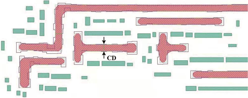
Fig. 1. CD of integrated circuit layout
![(a) Sketch of imaging process and (b) diagram of structure for DUV immersion lithography tool[1]](/richHtml/lop/2022/59/9/0922008/img_02.jpg)
Fig. 2. (a) Sketch of imaging process and (b) diagram of structure for DUV immersion lithography tool[1]
Fig. 3. Schematic diagram of OPC. (a) Imaging process before and after OPC optimization[2]; (b) masks and their image results before and after OPC optimization[15]
Fig. 4. Schematic diagram of imaging processes using two different types of masks. (a) Binary mask; (b) Alt-PSM[2]
Fig. 5. Conventional illumination and common OAIs[2]. (a) Conventional circular illumination; (b) (c) dipole illuminations; (d) (e) quadrapole illuminations; (f) annular illumination
Fig. 6. Schematic diagram of imaging principle of lithography system[52]
Fig. 7. Comparison between thin-mask model and thick-mask model. (a) Kirchhoff approximation of photomask; (b) diffraction near-field model of thick mask[53]
Fig. 8. Schematic diagram of PE and EPE
Fig. 9. Schematic diagram of process windows[82]. (a) Rectangular process window; (b) elliptical process window
Fig. 10. Transformation and solution process of computational lithography problem[83]
Fig. 11. Different types of OPC methods. (a) Target pattern; (b) RBOPC result; (c) EBOPC result; (d) PBOPC result[109]
Fig. 12. Examples of RBOPC optimization results and correction rule tables[110]
Fig. 13. EBOPC method. (a) Optimization process of EBOPC; (b) image result after optimization[113]
Fig. 14. PBOPC simulation results based on SD algorithm. (a) Target pattern; (b) optimized gray mask; (c) optimized binary mask; (d)-(f) imaging results corresponding to mask patterns of first row[30]
Fig. 15. Comparison of ILT methods based on SD and CG algorithms. (a) Target pattern; (b) mask optimization result obtained by SD algorithm; (c) mask optimization result obtained by CG algorithm; (d)-(f) imaging results corresponding to mask patterns of first row [43]
Fig. 16. Comparison of PBOPC methods based on SIAOS and SGD. (a) Optimization results of mask and print image; (b) convergence curves[140]
Fig. 17. Comparison of ILT optimization results based on Adam and SGD algorithms. (a) Sarget pattern; (b) mask optimization result based on Adam algorithm; (c) mask optimization result based on SGD algorithm; (d) convergence curves of these two algorithms; (e) print image of Adam algorithm; (f) print image of SGD algorithm[157]
Fig. 18. Comparison of optimization results between PBSO and parametric SO. (a) Mask pattern; (b) dipole illumination obtained by parametric SO; (c) source optimization result obtained by PBSO; (d) cross-sections of aerial images; (e) process windows[163]
Fig. 19. SMO technique and its improvement on process window[25]
Fig. 20. SMO workflow for full-chip layout optimization[4]
Fig. 21. Optimization results and convergence curves of the SISMO, SESMO, and HSMO algorithms [52]
Fig. 22. Optimization results and convergence curve of PBSMO algorithm[42]
Fig. 23. Comparison of SMO optimization results between ALM algorithm and CG algorithm. (a)-(f) Optimized sources, masks, and print images obtained by ALM algorithm and CG algorithm, respectively; (g) average process windows obtained by two algorithms[44]
Fig. 24. Comparison of SMO simulation results among SD algorithm, conventional level-set algorithm, and narrow-band level-set algorithm. (a)-(l) Optimization results of sources, masks, and print images based on three algorithms; (m) convergence curves of these algorithms[192]
Fig. 25. Comparison of simulation results between traditional SMO and robust hybrid SMO algorithms (considering the influence of source blur and flare). (a) (f) Source optimization results; (b) (g) mask optimization results; (c) (h) print images under ideal parameters; (d) (i) print images influenced by the source blur (standard deviation of source blur σJ=0.05); (e) (j) print images influenced by the flare (flare ratio S=2%)[197]
Fig. 26. Compressive measurement process and reconstruction process of the linear CS[202]
Fig. 27. Comparison of fast SO techniques based on diffraction subspace method and ACS method (L is the function dimensionality after compression). (a)-(h) Source optimization results and imaging results; (i) (j) process windows[210]
Fig. 28. Comparison of the fast SO techniques based on the LCS, ACS, CG, and PSO algorithms[174]
Fig. 29. Comparison of simulation results for two nonlinear CS-OPC methods (K is the compression ratio). (a)-(h) Mask optimization results and print image results for different methods; (i) convergence curves of the cost functions; (j) process windows[216]
Fig. 30. Typical optimization examples of the CS-SMO algorithms. (a)-(d) Source patterns; (e)-(h) mask patterns; (i)-(l) print images[218]
Fig. 31. Simulation results of the fast OPC method based on adaptive kernel regression at 45 nm metal layer. (a) Corrected mask pattern; (b) optimized lithography image[49]
Fig. 32. Comparison of the fast EUV lithography mask diffraction near-field calculation methods (from left to right, it uses the rigorous electromagnetic field method, non-parametric kernel regression method, Kirchhoff approximation method, and DDM method). (a) Mask diffraction matrices obtained by different methods; (b) error maps of mask diffraction matrices[65]
Fig. 33. Prediction method and results of the etch bias based on neural network. (a) Features of mask pattern are extracted and inputted into the neural network to predict the etching bias; (b) comparison between measured etch bias and predicted etch bias[232]
Fig. 34. Fast mask optimization method based on the GAN-OPC model, where OPC layout is outputted by generator[105]
Fig. 35. Sketch of fast mask diffraction near-field calculation method based on FCN[67]
Fig. 36. Layout hotspot detection based on the CNN model[104]
Fig. 37. Designed masks and their print images obtained by MCNN[106]
Fig. 38. Comparison of the simulation results between SMO algorithm and SMPO algorithm. (a)-(d) Simulation result before optimization; (e)-(p) simulation results of SMO, SISMPO, and SESMPO algorithms[254]
Fig. 39. Workflow of DTCO[267]
Fig. 40. Expected development situation of the pitch sizes of some key devices on the chip[271]
Fig. 41. Sketch of EUV lithography system[274]
Fig. 42. Mask correction results and algorithm convergence curves for defects at different positions (mask defects locate at the center, edge, and corner of the pattern, respectively) [95]
Fig. 43. Simulation results of the EUV-SMO methods based on pixelated source model. (a)-(c) Source, mask, and print image obtained by the SMO algorithm; (d)-(f) source, mask, and print image obtained by the “SMO+Retargeting” method[275]


Set citation alerts for the article
Please enter your email address

© Copyright 2018-2021 | Chinese Laser Press. All Rights Reserved 沪ICP备15018463号-20