• Journal of Semiconductors
  • Vol. 41, Issue 10, 102802 (2020)
R. Singh1, T. R. Lenka1, R. T. Velpula2, B. Jain2..., H. Q. T. Bui2 and H. P. T. Nguyen2|Show fewer author(s)
Author Affiliations
  • 1Department of Electronics & Communication Engineering, National Institute of Technology Silchar, AS, 788010, India
  • 2Department of Electrical and Computer Engineering, New Jersey Institute of Technology, Newark, NJ, 07102, USA
  • show less
    DOI: 10.1088/1674-4926/41/10/102802 Cite this Article
    R. Singh, T. R. Lenka, R. T. Velpula, B. Jain, H. Q. T. Bui, H. P. T. Nguyen. Investigation of current collapse and recovery time due to deep level defect traps in β-Ga2O3 HEMT[J]. Journal of Semiconductors, 2020, 41(10): 102802 Copy Citation Text show less
    (Color online) Schematic cross sectional view of the analysed device structure.
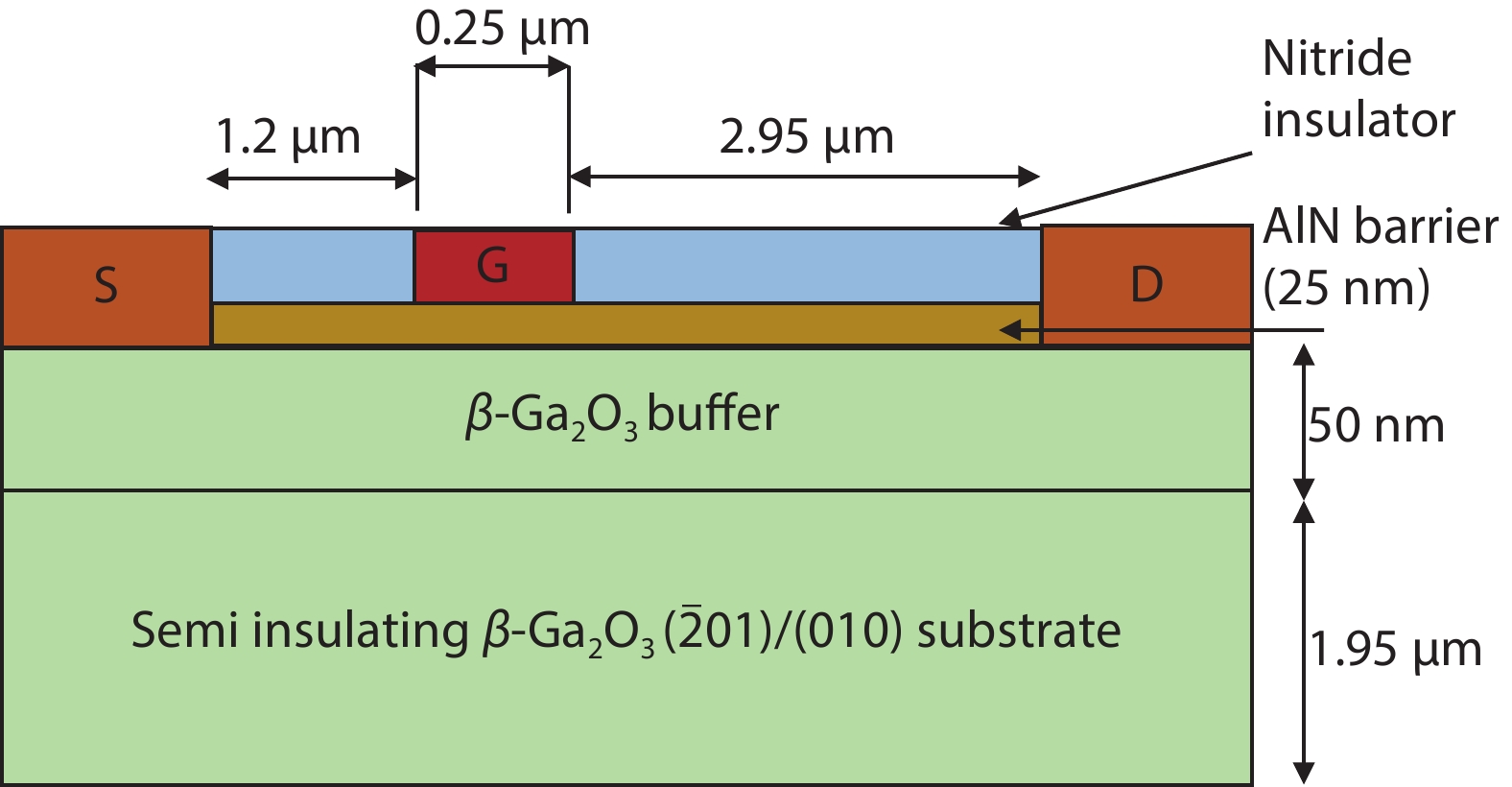
    Fig. 1. (Color online) Schematic cross sectional view of the analysed device structure.
    (Color online) Pre-stress and post-stress bias voltages at gate and drain terminals.
    Fig. 2. (Color online) Pre-stress and post-stress bias voltages at gate and drain terminals.
    (Color online) Pre-stress and post-stress drain current. Inset: current collapse.
    Fig. 3. (Color online) Pre-stress and post-stress drain current. Inset: current collapse.
    (Color online) Trapping and de-trapping of defect trap under gate stress.
    Fig. 4. (Color online) Trapping and de-trapping of defect trap under gate stress.
    (Color online) Drain stress and recovery of current recovery due to de-population of traps.
    Fig. 5. (Color online) Drain stress and recovery of current recovery due to de-population of traps.
    (Color online) Current collapse and recovery curve, showing intentional doped Fe causes most of the current collapse and Ge doping caused current collapse takes approximately 2 h to attain steady state value.
    Fig. 6. (Color online) Current collapse and recovery curve, showing intentional doped Fe causes most of the current collapse and Ge doping caused current collapse takes approximately 2 h to attain steady state value.
    (Color online) Ionised trap density horizontally at a depth of 0.5 μm in the substrate.
    Fig. 7. (Color online) Ionised trap density horizontally at a depth of 0.5 μm in the substrate.
    ReferenceTrap energy levels (eV) Capture cross section (10−14 cm–2) Trap sourceTrap concentration (1015 cm–3) Current collapse/ recovery time
    [12] EC – 0.78 0.7Fe-doped substrate ( 01) 10Moderate/ few seconds
    EC – 0.75 5Fe-doped substrate ( 01) 10Moderate/ few minutes
    [9] EC – 0.98 0.1− 9Ge-doped PAMBE on (010) substrate1.6Mild/ ~ 1 h
    [10] EC – 0.82 1UID bulk EFG wafer (010)36Severe/ ~ 10 min
    Table 1. Deep level traps reported in β-Ga2O3 substrate and epitaxial layer, energy level, capture cross section and trap concentration. Fe and Ge enabled current collapse and drain current recovery time to pre-stress condition.
    R. Singh, T. R. Lenka, R. T. Velpula, B. Jain, H. Q. T. Bui, H. P. T. Nguyen. Investigation of current collapse and recovery time due to deep level defect traps in β-Ga2O3 HEMT[J]. Journal of Semiconductors, 2020, 41(10): 102802
    Download Citation