
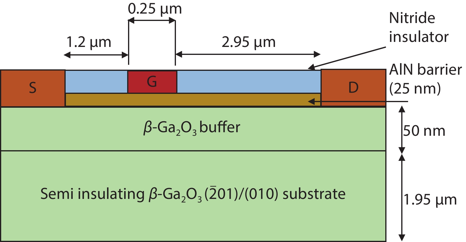
R. Singh, T. R. Lenka, R. T. Velpula, B. Jain, H. Q. T. Bui, H. P. T. Nguyen. Investigation of current collapse and recovery time due to deep level defect traps in β-Ga2O3 HEMT[J]. Journal of Semiconductors, 2020, 41(10): 102802
- Journal of Semiconductors
- Vol. 41, Issue 10, 102802 (2020)
Abstract
| () |
View in Article


Set citation alerts for the article
Please enter your email address

© Copyright 2018-2021 | Chinese Laser Press. All Rights Reserved 沪ICP备15018463号-20