
R. Singh, T. R. Lenka, R. T. Velpula, B. Jain, H. Q. T. Bui, H. P. T. Nguyen. Investigation of current collapse and recovery time due to deep level defect traps in β-Ga2O3 HEMT[J]. Journal of Semiconductors, 2020, 41(10): 102802
- Journal of Semiconductors
- Vol. 41, Issue 10, 102802 (2020)
Abstract
1. Introduction
There has recently been considerable interest in monoclinic β-phase of gallium oxide (β-Ga2O3) inspired by its excellent material characteristics—large energy bandgap EG ~ 4.9 eV[
Several experimental studies on defects throughout the entire bandgap of β-Ga2O3 (010) layers have used deep level transient spectroscopy (DLTS) and deep level optical spectroscopy (DLOS) techniques[
With the distinct trap level defects reported so far, device performance can be easily questioned unless different trap sources and their individual effects on specific output parameters are fully established because device degradation may be reversible or permanent in nature. Significant progress in Ga2O3 based electronic devices such as Schottky diodes[
Potential application of β-Ga2O3 based devices beg the question of whether the device degradation due to various traps EC – 0.98, 0.82, 0.78, 0.75 eV[
2. Device structure and simulation framework
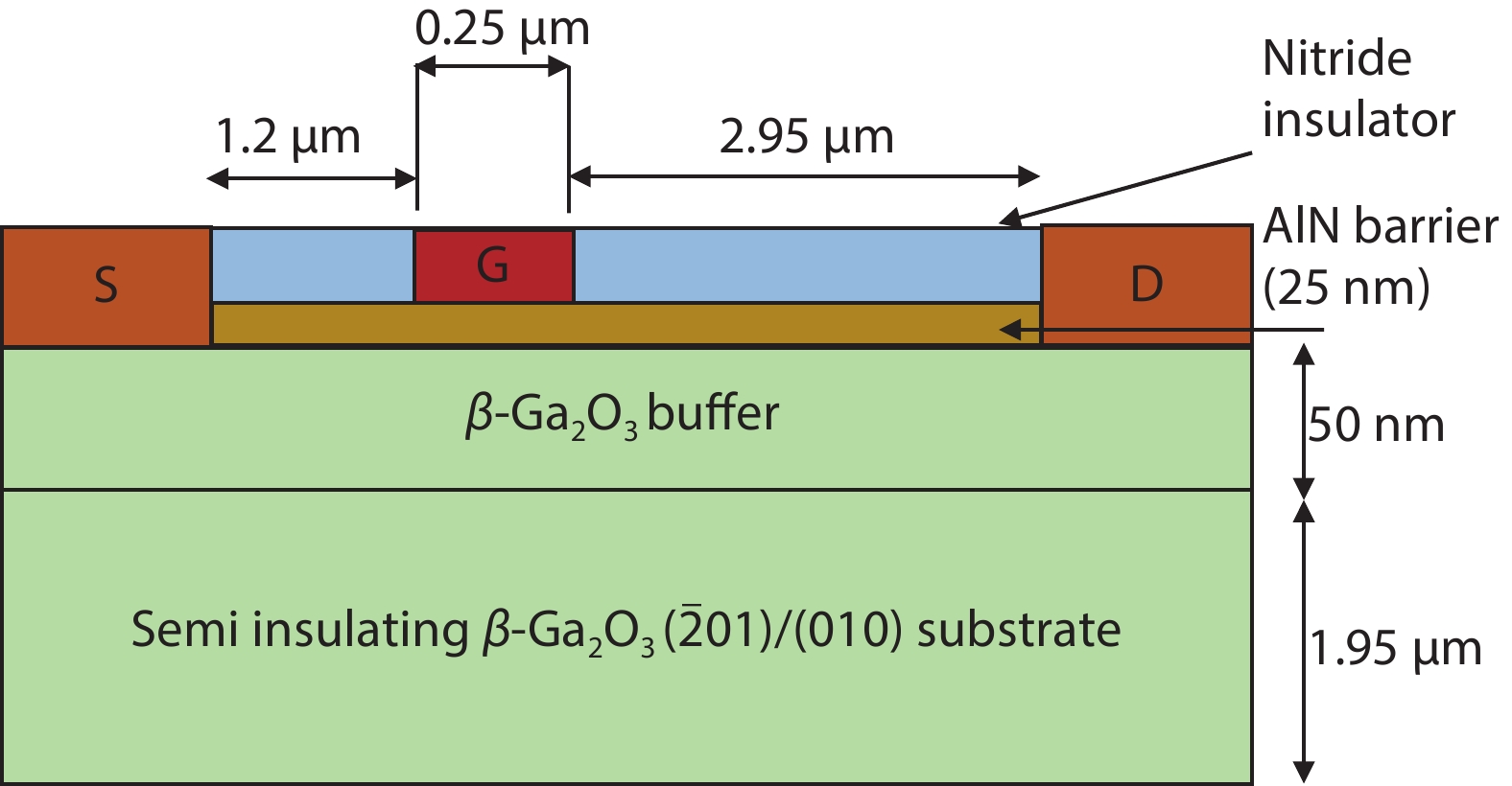
Fig. 1 shows device structure of AlN/β-Ga2O3 HEMT which is analysed in this report. The sequence of materials comprise of 25 nm AlN barrier layer on 2 μm β-Ga2O3 substrate. Gate material of Au/Ni with gate length, LG of 0.25 μm and Schottky barrier height of 0.8 eV is set by fixing the work function, ϕM of the gate metal of 2.2 eV, electron affinity of the AlN barrier is set as 1.4 eV[
![]()
Figure 1.(Color online) Schematic cross sectional view of the analysed device structure.
Using electron and hole effective masses of β-Ga2O3[
For undoped AlN layer default material parameters as mentioned in Ref. [22] are considered except electron affinity (χ = 1.4 eV). Due to low in-plane lattice mismatch between AlN/β-Ga2O3 heterojunction, spontaneous and piezoelectric polarization built in model[
Based on previous published reports[
3. Results and discussions
The proposed device is analysed under three different conditions—gate stress, drain stress, and gate–drain stress. In all three bias conditions, device is biased in low stress and high stress state for 0.1 to 1 ms with respective DC bias at the gate and drain terminals. During initial bias condition, the device is simulated for output drain current under DC bias at gate and drain terminal. After applying a DC bias of VGS = 0 V and VDS = 5 V, this initial bias condition is maintained for 1 ms in dynamic mode. Then, the device is pulsed into high stress state, −25 V on the gate (in gate stress condition); 25 V on the drain terminal (in drain stress); and −25 to 25 V on the gate and drain terminals respectively for another 1 ms, as shown in Fig. 2. Then, the device is returned to its original bias condition. Since we are analysing the recoverable current collapse phenomenon which is not permanent in nature[
![]()
Figure 2.(Color online) Pre-stress and post-stress bias voltages at gate and drain terminals.
![]()
Figure 3.(Color online) Pre-stress and post-stress drain current. Inset: current collapse.
To analyse the effect of these deep level traps under gate-stress condition, the drain bias remains at fixed bias of 5 V; the device is driven into pinch-off (high stress at gate –25 V for 1 ms) followed by steady state bias. The resulting drain current collapse and recovery time is shown in Fig. 4. It is evident that current degrades momentarily and almost full current recovery happens at time t = 2 ms.
![]()
Figure 4.(Color online) Trapping and de-trapping of defect trap under gate stress.
Similar steps are performed to simulate the device under drain stress with appropriate drain and gate bias and the results are shown in Fig. 5. Due to the low concentration (1014 cm−3) of deep level traps at EC − 0.1 eV, − 0.2 eV in Ge-doped epitaxial layer there is no current collapse phenomenon observed. In gate and drain stress bias conditions, both terminals are put in high stress for 1 ms with − 25 V at gate and 25 V at drain terminal. The results are shown in Fig. 6. Current collapse is evident mainly due to traps at EC –0.82 eV with recovery time of almost 10 min. The trap level at EC – 0.98 eV demonstrated in Ge-doped epitaxial layer contributes negligibly in current collapse, but steady state drain current restores after a time elapse of 1 h. The other two trap levels EC – 0.75 eV, 0.78 eV show significant current collapse and recovery time of few seconds to few minutes are quantified respectively, the later one having large capture cross section of 10−14 cm−2.
![]()
Figure 5.(Color online) Drain stress and recovery of current recovery due to de-population of traps.
![]()
Figure 6.(Color online) Current collapse and recovery curve, showing intentional doped Fe causes most of the current collapse and Ge doping caused current collapse takes approximately 2 h to attain steady state value.
The ionized Fe trap occupancy before and after high stress bias condition highlights are shown in Fig. 7. It can be seen that the trap density under the gate and gate source area near the surface mostly affects the current degradation. Ionization trap density is plotted at a depth of 0.5 μm from the surface in the β-Ga2O3 substrate. There is a significant difference in the occupancy of trap along the depth in the substrate and along the horizontal direction towards gate. The gate length of the analysed device, LG of 0.25 μm, and the effect of Fe trap occupancy extends along the depth up to 0.5 μm (two times of gate length), and along source and drain regions. Source, gate, and drain electrodes are shown in upper part of Fig. 7 to correlate device dimension with ionized trap density in the substrate.
![]()
Figure 7.(Color online) Ionised trap density horizontally at a depth of 0.5
4. Conclusion
The trapping effects led current collapse phenomenon using drain transient characteristics of β-Ga2O3 HEMT is presented. The recovery time for the drain current to return to its steady state value is investigated using Atlas TCAD simulations. The trap level at energy EC – 0.8 eV in Fe-doped β-Ga2O3 substrate plays crucial role in undesirable current collapse phenomenon and the recovery time is about 10 min. In the Ge-doped β-Ga2O3 epitaxial layer, the trap level at EC – 0.98 eV insignificantly degrades the drain current but takes roughly 1 h to restore the original value. This current degradation is reversible event and current returns to its steady state value but only after a finite time varying from few seconds to several minutes depending on the trap characteristics. It is also observed that unintentional interface traps have a negligible effect on current collapse. The report thoroughly establishes that intentional Fe-doping in semi insulating β-Ga2O3 substrate led traps cause current collapse, and on the other side recovery time in current lag in Ge-doped β-Ga2O3 epitaxial layer is approximately 1 h. By measuring the current recovery time, this report effectively distinguishes between temporary and permanent device degradation due to current collapse. The findings of this work may be useful in reliability study of β-Ga2O3 devices.
Acknowledgements
This publication is an outcome of the collaborative R&D work undertaken in the project under the Visvesvaraya PhD Scheme of Ministry of Electronics & Information Technology, Govt. of India, being implemented by Digital India Corporation.
References
[1] H Y He, R Orlando, M A Blanco et al. First-principles study of the structural, electronic, and optical properties of Ga2O3in its monoclinic and hexagonal phases. Phys Rev B, 74, 195123(2006).
[2] M Higashiwaki, K Sasaki, A Kuramata et al. Gallium oxide (Ga2O3) metal–semiconductor field-effect transistors on single-crystal
[3] K Ghosh, U Singisetti. Ab initio velocity-field curves in monoclinic
[4] J B Varley, J R Weber, A Janotti et al. Oxygen vacancies and donor impurities in
[5] E Chikoidze, A Fellous, A Perez-Tomas et al. P-type
[6] A Kyrtsos, M Matsubara, E Bellotti. On the feasibility of p-type Ga2O3. Appl Phys Lett, 112, 032108(2018).
[7] Y Tomm, P Reiche, D Klimm et al. Czochralski grown Ga2O3 crystals. J Cryst Growth, 220, 510(2000).
[8] H Aida, K Nishiguchi, H Takeda et al. Growth of
[9] E Farzana, E Ahmadi, J S Speck et al. Deep level defects in Ge-doped (010)
[10] Z Zhang, E Farzana, A R Arehart et al. Erratum: “Deep level defects throughout the bandgap of (010)
[11] K Irmscher, Z Galazka, M Pietsch et al. Electrical properties of
[12] M E Ingebrigtsen, J B Varley, A Y Kuznetsov et al. Iron and intrinsic deep level states in Ga2O3. Appl Phys Lett, 112, 042104(2018).
[13] K Sasaki, M Higashiwaki, A Kuramata et al. Ga2O3 Schottky barrier diodes fabricated by using single-crystal
[14] S Krishnamoorthy, Z B Xia, S Bajaj et al. Delta-doped
[15] H Zhou, K Maize, G Qiu et al.
[16] T Oshima, Y Kato, N Kawano et al. Carrier confinement observed at modulation-doped
[17] Y W Zhang, A Neal, Z B Xia et al. Demonstration of high mobility and quantum transport in modulation-doped
[18] J F McGlone, Z B Xia, Y W Zhang et al. Trapping effects in Si
[19] A Y Polyakov, N B Smirnov, I V Shchemerov et al. Defect states determining dynamic trapping-detrapping in
[20] H D Sun, C G Torres Castanedo, K K Liu et al. Valence and conduction band offsets of
[21] A Mock, R Korlacki, C Briley et al. Band-to-band transitions, selection rules, effective mass, and excitonic contributions in monoclinic
[22]
[23]
[24]


Set citation alerts for the article
Please enter your email address

© Copyright 2018-2021 | Chinese Laser Press. All Rights Reserved 沪ICP备15018463号-20