• Journal of Semiconductors
  • Vol. 41, Issue 7, 072902 (2020)
Xiuxin Xia1、2, Xiaoxi Li1、2, and Hanwen Wang1、2
Author Affiliations
  • 1Shenyang National Laboratory for Materials Science, Institute of Metal Research, Chinese Academy of Sciences, Shenyang 110016, China
  • 2School of Material Science and Engineering, University of Science and Technology of China, Hefei 230026 China
  • show less
    DOI: 10.1088/1674-4926/41/7/072902 Cite this Article
    Xiuxin Xia, Xiaoxi Li, Hanwen Wang. Metal–insulator transition in few-layered GaTe transistors[J]. Journal of Semiconductors, 2020, 41(7): 072902 Copy Citation Text show less
    (Color online) Characterizations of GaTe and a typical BN/GaTe/BN device. (a) Schematic of GaTe layered lattice, with the interlayer spacing of ~0.8 nm. (b) Schematic illustration of the device. (c) Optical micrograph of the device, the scale bar is 10 µm. (d) AFM morphology image of the device with a height profile plotted in (e), plotted along the green dashed line in (d).
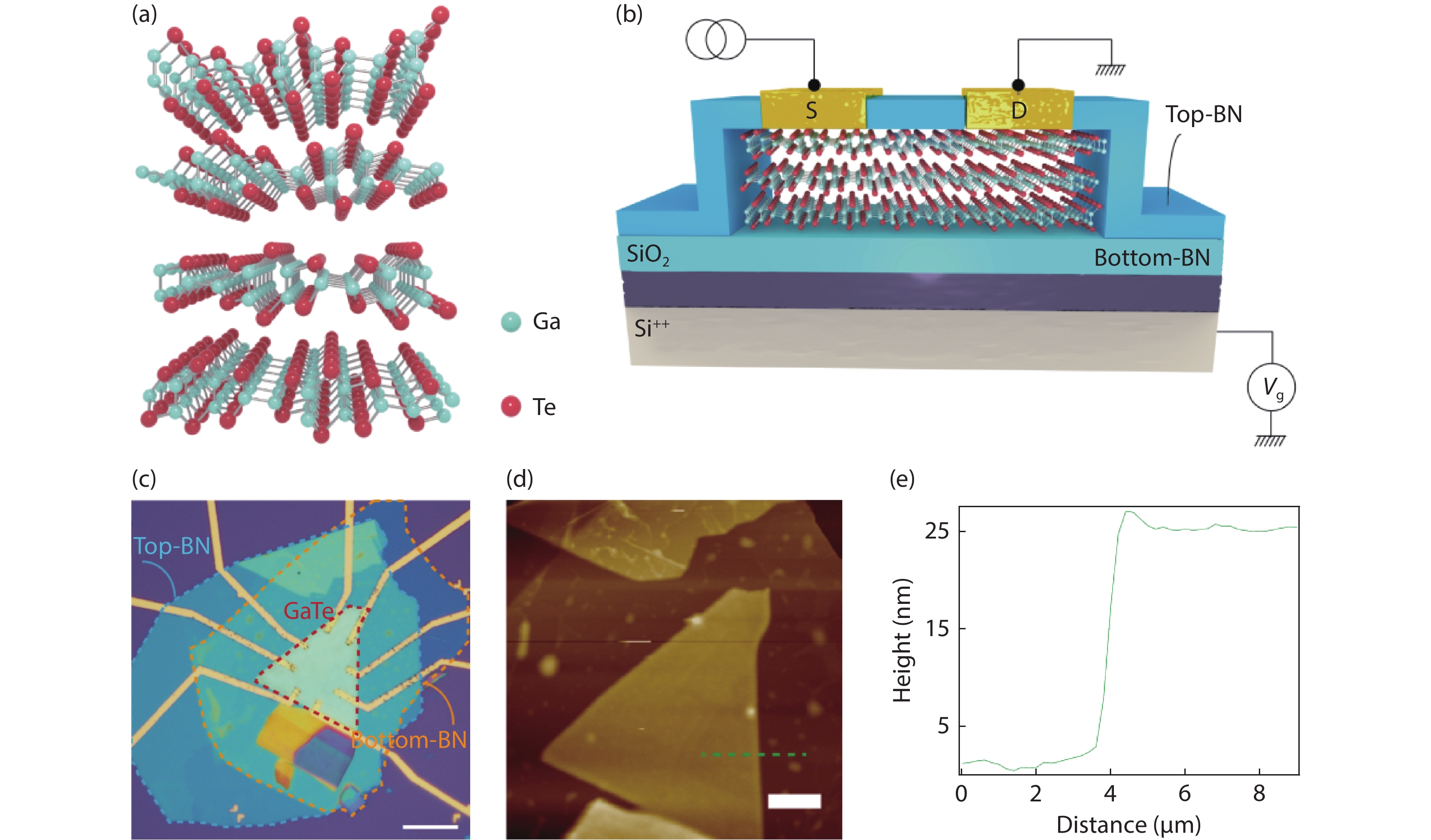
    Fig. 1. (Color online) Characterizations of GaTe and a typical BN/GaTe/BN device. (a) Schematic of GaTe layered lattice, with the interlayer spacing of ~0.8 nm. (b) Schematic illustration of the device. (c) Optical micrograph of the device, the scale bar is 10 µm. (d) AFM morphology image of the device with a height profile plotted in (e), plotted along the green dashed line in (d).
    (Color online) Electrical transport properties of BN/GaTe/BN devices at room temperature. (a) Field effect curve at Vds = 2 V of the device. (b) The same data plotted in a log scale. (c) Ids–Vds curves on the hole side at fixed gate voltages. (d) Ids–Vds curves on the electron side at fixed gate voltages.
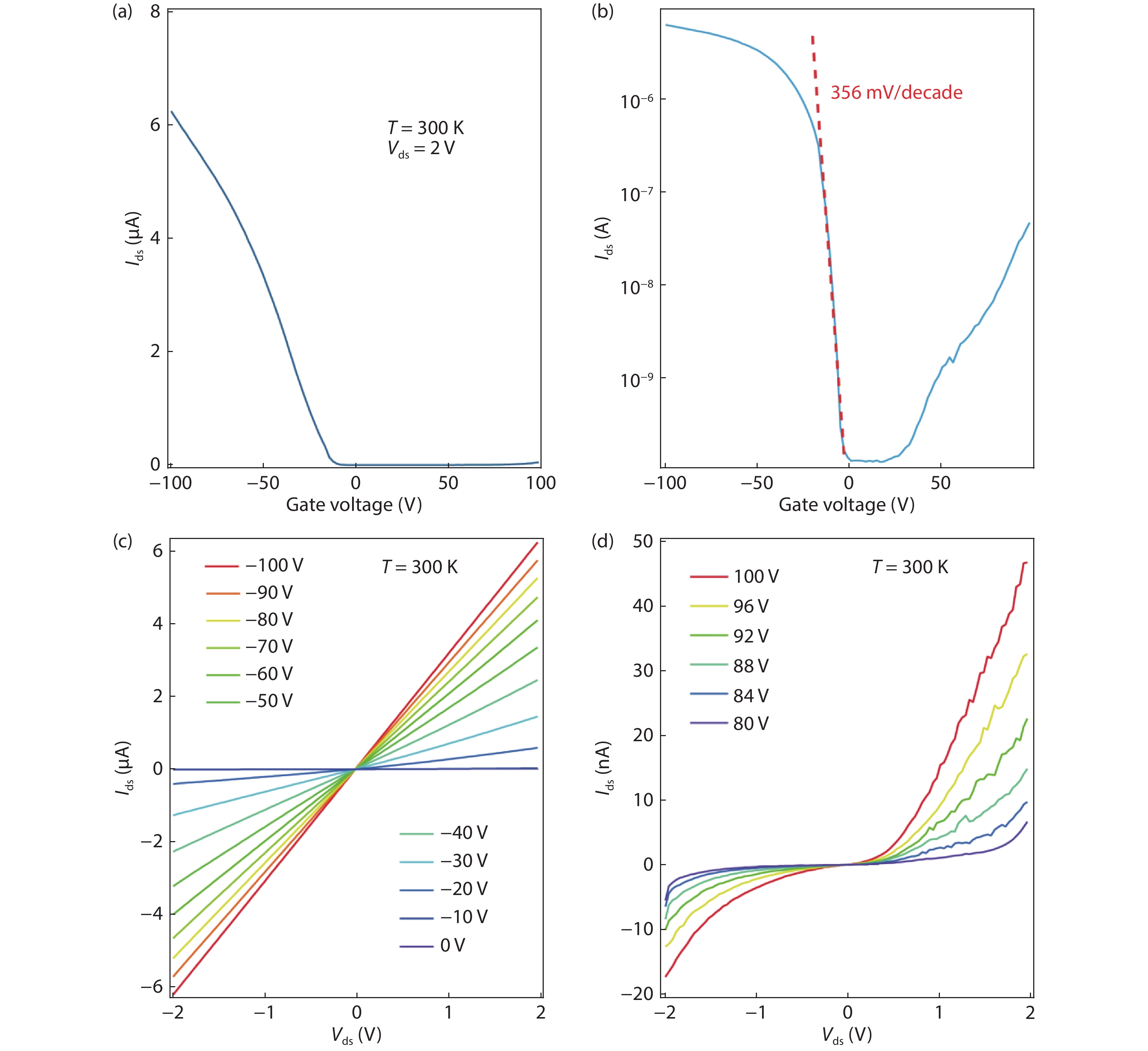
    Fig. 2. (Color online) Electrical transport properties of BN/GaTe/BN devices at room temperature. (a) Field effect curve at Vds = 2 V of the device. (b) The same data plotted in a log scale. (c) IdsVds curves on the hole side at fixed gate voltages. (d) IdsVds curves on the electron side at fixed gate voltages.
    (Color online) Transport properties of BN/GaTe/BN devices at different temperatures. (a) Color map of I–V curves as a function of gate voltage at different temperatures. To enhance the visibility, color scales are set to cutoffs at ±1 nA. (b, c) Line cuts in (a), with output curves on hole and electron sides, respectively.
    Fig. 3. (Color online) Transport properties of BN/GaTe/BN devices at different temperatures. (a) Color map of I–V curves as a function of gate voltage at different temperatures. To enhance the visibility, color scales are set to cutoffs at ±1 nA. (b, c) Line cuts in (a), with output curves on hole and electron sides, respectively.
    (Color online) Temperature-dependent transport characteristics in few-layered GaTe device with a constant voltage Vds = 2 V. (a) T-dependence of conductivity σ for different gate voltages. (b) Ids–Vg at different temperatures, Ids increases when the temperature decreases at high negative gate voltage Vg < −30 V. (c) Field-effect mobility as a function of temperature. The solid black line is best fitted to the power law in the range of 100–250 K.
    Fig. 4. (Color online) Temperature-dependent transport characteristics in few-layered GaTe device with a constant voltage Vds = 2 V. (a) T-dependence of conductivity σ for different gate voltages. (b) IdsVg at different temperatures, Ids increases when the temperature decreases at high negative gate voltage Vg < −30 V. (c) Field-effect mobility as a function of temperature. The solid black line is best fitted to the power law in the range of 100–250 K.
    Xiuxin Xia, Xiaoxi Li, Hanwen Wang. Metal–insulator transition in few-layered GaTe transistors[J]. Journal of Semiconductors, 2020, 41(7): 072902
    Download Citation