
Xiuxin Xia, Xiaoxi Li, Hanwen Wang. Metal–insulator transition in few-layered GaTe transistors[J]. Journal of Semiconductors, 2020, 41(7): 072902
- Journal of Semiconductors
- Vol. 41, Issue 7, 072902 (2020)
Abstract
1. Introduction
Since the discovery of graphene[
Recently, telluride gallium (GaTe) has attracted increasing attentions. As a 2D layered semiconductor with a direct band gap, GaTe shows excellent photoelectric properties[
In this work, we report measurements on the transport properties of GaTe at different temperatures. It is known that GaTe is easily oxidized in air. Therefore, to attenuate damages from the air environment, h-BN was employed to fully encapsulate GaTe by the dry transfer method performed in a glove box. The results show that by tuning the carrier density, the GaTe devices exhibit ambipolar transport property, which persists down to low temperatures. As temperature decreases, our devices display a remarkable increase in the field-effect mobilities on the hole side: from ~40 cm2V−1s−1 at 300 K to ~1200 cm2V−1s−1 at 3 K, respectively. Moreover, for gate voltage approaching −100 V, all devices studied show a metallic behavior over the entire T-range. These studies provide us with a measure to understand the transport properties of thin flakes of GaTe, which may enable the design of future electronic and optoelectronic devices based on it.
2. Method
2.1. Crystal growth and characterization
Bulk crystals were grown via self-flux method[
2.2. Exfoliation of GaTe and fabrication of few-layered GaTe transistors
Thin flakes of GaTe were obtained through a mechanical exfoliation method. Bottom h-BN was directly exfoliated onto the substrate. Selected GaTe flakes and top h-BN were stacked in sequence by dry transfer procedure[
2.3. Measurements on electrical transport
Electrical measurements were performed by micro-probe station and physical properties measurement system (PPMS) with Keithley 2400 source meters and digital lock-in amplifiers Stanford Research Systems SR830.
3. Results and discussion
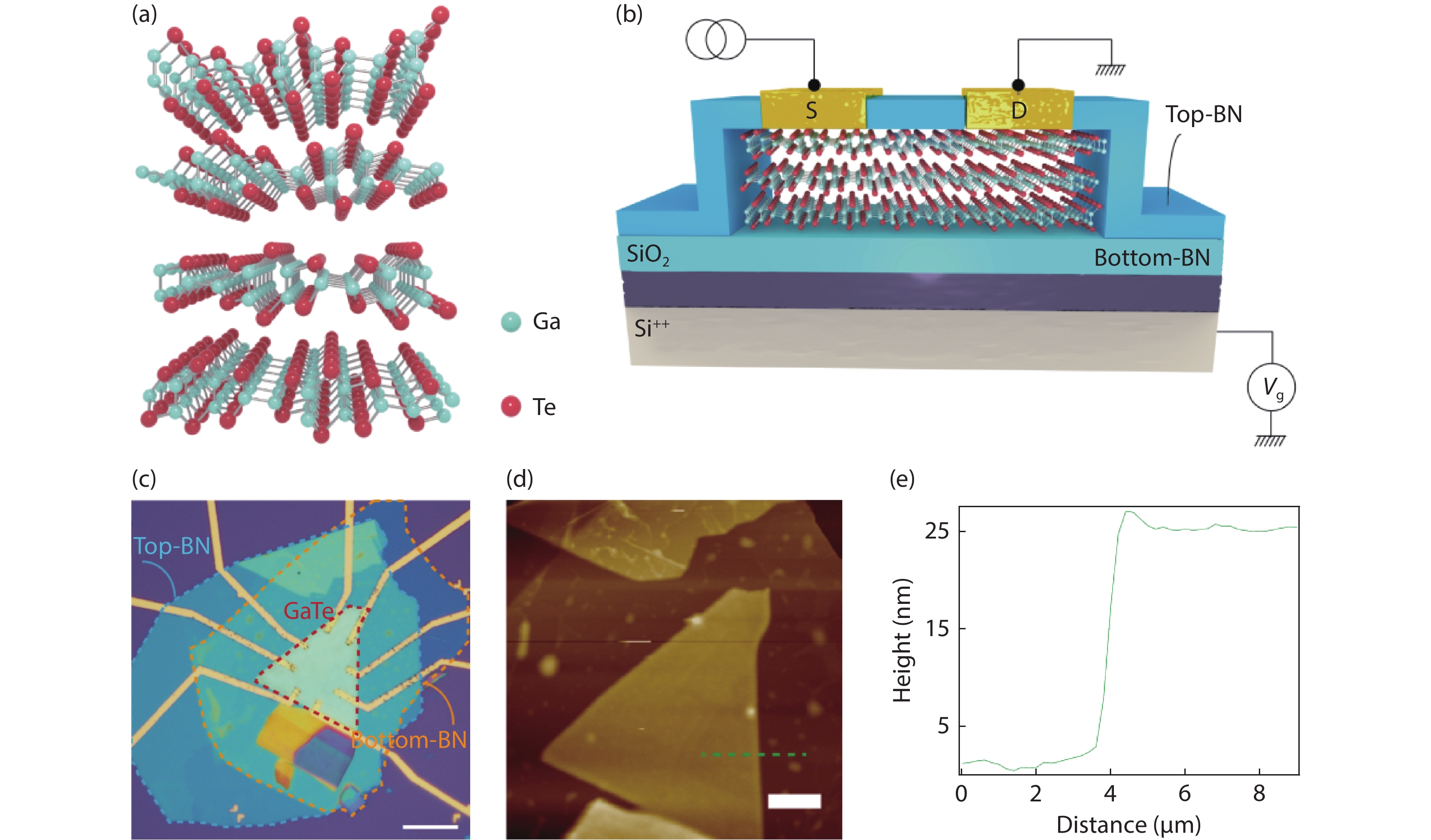
As a layered material, the in-plane interaction of GaTe is covalent bondings while van der Waals force keeps the layers together along the c-axis, and the interlayer spacing is ~0.8 nm. Fig. 1(a) shows the schematic of GaTe crystal structure which is monoclinic lattice with low symmetry. Devices of thin flakes of GaTe were fabricated by the van der Waals stacking process. A configuration of such a device is depicted in Fig. 1(b), where few-layered GaTe flakes were sandwiched by two hexagonal boron nitride (h-BN) layers with a thickness of about 20 nm.
![]()
Figure 1.(Color online) Characterizations of GaTe and a typical BN/GaTe/BN device. (a) Schematic of GaTe layered lattice, with the interlayer spacing of ~0.8 nm. (b) Schematic illustration of the device. (c) Optical micrograph of the device, the scale bar is 10
Due to its insulating and inert properties, h-BN serves as a proper dielectric layer and provides preservation of GaTe for its intrinsic properties. Layered h-BN can also provide an atomically flat substrate which is conducive to improving the performance of the device. We have performed systematic measurements on multiple devices and most of them exhibit similar behaviours. We will mainly discuss the representative device here, an optical micrograph is shown in Fig. 1(c), thin flake of GaTe is highlighted with red dashed line. Fig. 1(d) shows the atomic force migraph (AFM) scan, corresponding to the heterostructure in Fig. 1(c). It can be seen that the surface of the sample obtained by dry transfer is quite clean and flat. GaTe flake in this device is ~24.5 nm (Fig. 1(e)).
Fig. 2(a) displays the transfer characteristics of the device at T = 300 K; i.e., the source-drain current Ids dependence on the gate voltage Vg in the range of ±100 V. A typical p-type FET behaviour can be observed which is similar with other reports, at the hole side, an ”ON/OFF” ratio of ~104 and a subthreshold swing (SS) of ~356 mV/dec can be extracted from the curve. Further improvement for the SS might be achieved by employing graphite and h-BN as the gate electrode and dielectric layer, respectively. Surprisingly, when taking a closer look at the transfer curves in the range of Vg > 70 V, we can see the device also slightly turns on which is more obvious when plotted in log scale (shown in Fig. 2(b)), which is the hallmark of a bipolar behaviour. To better characterize the performance of the device, we performed output tests. As can be seen in Fig. 2(c), the device turns on as Vg < −20 V and linear Ids–Vds curves at different fixed Vg indicate that Ohmic contacts have been achieved on the hole side. For the electron side, the device turns on as Vg > 80 V, which further indicates that ambipolar transport is realized, suggesting GaTe will be a good candidate for being used in multi-functional devices such as p–n juctions and tunnel diodes. In contrast, the Ids–Vds curves on the electron side largely deviate from linear behaviour and the “ON” current is relatively weak. Further enhancement of the transport properties on the electron side may be realized by trying high-κ dielectric layer[
![]()
Figure 2.(Color online) Electrical transport properties of BN/GaTe/BN devices at room temperature. (a) Field effect curve at
In Fig. 3, we display the transport properties of the device at different temperatures. Fig. 3(a) shows the color map of Ids–Vds curves as a function of gate voltage at different temperatures. The distinct behaviour of a bipolar FET can be observed at all temperatures suggesting the ambipolar transport property is quite robust while the gap becomes a little larger on lowering the temperature. As can be seen in Fig. 3(b), the Ids–Vds curve remains linear at 50 K while slightly deviate from linear below 50 K. Furthermore, it is of a surprise to see that the “ON” current becomes much higher at low temperature. However, similar increasement of current was not observed on the electron side, see Fig. 3(c).
![]()
Figure 3.(Color online) Transport properties of BN/GaTe/BN devices at different temperatures. (a) Color map of
We now examine the transport characteristics of few-layered GaTe device at various temperatures in more detail. Fig. 4(a) presents the conductivity (σ) plotted in the unit of quantum conductance (e2/h). Clear metal-insulator transition (MIT) behavior can be seen because the device has metallic ground state with a residual resistance at hole doping (Vg = –40 V, for example), while it enters insulating regime when Vg approaches to 0 V. As shown in Fig. 4(b), with increased hole doping, the output curves of the device display a crossover from an insulating regime at higher gate voltage (Vg > −30 V), where Ids increases with the temperature increasing, to a metallic regime at lower gate voltage (Vg < −30 V), where Ids increases as the temperature decreases. Similar behaviour has been observed in multiple few-layered GaTe devices. This MIT phenomenon was observed for the first time in GaTe flakes, and our results are consistent with previous studies on WSe2, MoS2, WS2[
![]()
Figure 4.(Color online) Temperature-dependent transport characteristics in few-layered GaTe device with a constant voltage
To further understand this, we plot the field-effect mobility in the metallic regime (Vg = −40 V) as a function of temperature using the expression
4. Conclusion
Fabricating few-layered GaTe tansistors encapsulated in h-BN offers more opportunities for intrinsic properties research with GaTe. Transport measurements of GaTe FETs have proven that GaTe could serve as a platform for electronic systems thanks to its formidable ability in carrier modulation. Metal-insulator transition has been achieved in thin flakes of GaTe with a Si back gate. In addition, ambipolar behaviour was also observed in our devices making it promising for the implementation of nanoelectronic systems that envolves semiconducting channels. Our findings manifest the potential of GaTe for future functional devices based on it.
Acknowledgements
This work is supported by the the National Natural Science Foundation of China (NSFC, Grant Nos. 11974357, and U1932151), the State Key Research Development Program of China (Grant No. 2019YFA0307800).
References
[1] K S Novoselov, A K Geim, S V Morozov et al. Electric field effect in atomically thin carbon films. Science, 306, 666(2004).
[2] A K Geim, I V Grigorieva. Van der Waals heterostructures. Nature, 499, 419(2013).
[3] Y Liu, N O Weiss, X Duan et al. Van der Waals heterostructures and devices. Nat Rev Mater, 1, 1(2016).
[4] Y Saito, Y Iwasa. Ambipolar insulator-to-metal transition in black phosphorus by ionic-liquid gating. ACS Nano, 9, 3192(2015).
[5] Z Wang, T Zhang, M Ding et al. Electric-field control of magnetism in a few-layered van der Waals ferromagnetic semiconductor. Nat Nanotechnol, 13, 554(2018).
[6] R Saito, M Fujita, G Dresselhaus et al. Electronic structure of chiral graphene tubules. Appl Phys Lett, 60, 2204(1992).
[7] K F Mak, K L McGill, J Park et al. The valley Hall effect in MoS2 transistors. Science, 344, 1489(2014).
[8] B Huang, G Clark, D R Klein et al. Electrical control of 2D magnetism in bilayer CrI3. Nat Nanotechnol, 13, 544(2018).
[9] X Wang, J Tang, X Xia et al. Current-driven magnetization switching in a van der Waals ferromagnet Fe3GeTe2. Sci Adv, 5, eaaw8904(2019).
[10] N Mott. Metal–insulator transition. Rev Mod Phys, 40, 677(1968).
[11] S Kravchenko, D Simonian, M Sarachik et al. Electric field scaling at a
[12] A J Frenzel, A S McLeod, D Z R Wang et al. Infrared nanoimaging of the metal–insulator transition in the charge-density-wave van der Waals material 1T-TaS2. Phys Rev B, 97, 035111(2018).
[13] B Radisavljevic, A Kis. Mobility engineering and a metal–insulator transition in monolayer MoS2. Nat Mater, 12, 815(2013).
[14] L Ponomarenko, A Geim, A Zhukov et al. Tunable metal–insulator transition in double-layer graphene heterostructures. Nat Phys, 7, 958(2011).
[15] C Cen, S Thiel, G Hammerl et al. Nanoscale control of an interfacial metal–insulator transition at room temperature. Nat Mater, 7, 298(2008).
[16] C L Wu, H Yuan, Y Li et al. Gate-induced metal–insulator transition in MoS2 by solid superionic conductor LaF3. Nano Lett, 18, 2387(2018).
[17] P Patil, S Ghosh, M Wasala et al. Evidence of metal-insulator transition in 2D Van der Waals layers of copper indium selenide (CuIn7Se11). APS Meeting Abstracts(2019).
[18] G Duvjir, B K Choi, I Jang et al. Emergence of a metal–insulator transition and high-temperature charge-density waves in VSe2 at the monolayer limit. Nano Lett, 18, 5432(2018).
[19] Y Cao, V Fatemi, S Fang et al. Unconventional superconductivity in magic-angle graphene superlattices. Nature, 556, 43(2018).
[20] F Liu, H Shimotani, H Shang et al. High-sensitivity photodetectors based on multilayer GaTe flakes. ACS Nano, 8, 752(2014).
[21] S Huang, Y Tatsumi, X Ling et al. In-plane optical anisotropy of layered gallium telluride. ACS Nano, 10, 8964(2016).
[22] J Kang, V K Sangwan, H S Lee et al. Solution-processed layered gallium telluride thin-film photodetectors. ACS Photonics, 5, 3996(2018).
[23] Z Wang, M Safdar, M Mirza et al. High-performance flexible photodetectors based on GaTe nanosheets. Nanoscale, 7, 7252(2015).
[24] H Wang, M L Chen, M Zhu et al. Gate tunable giant anisotropic resistance in ultra-thin GaTe. Nat Commun, 10, 1(2019).
[25] H Cai, B Chen, G Wang et al. Synthesis of highly anisotropic semiconducting GaTe nanomaterials and emerging properties enabled by epitaxy. Adv Mater, 29, 1605551(2017).
[26] Z Wang, K Xu, Y Li et al. Role of Ga vacancy on a multilayer GaTe phototransistor. ACS Nano, 8, 4859(2014).
[27] A Castellanos-Gomez, M Buscema, R Molenaar et al. Deterministic transfer of two-dimensional materials by all-dry viscoelastic stamping. 2D Mater, 1, 011002(2014).
[28] J Feng, X Qian, C W Huang et al. Strain-engineered artificial atom as a broad-spectrum solar energy funnel. Nat Photonics, 6, 866(2012).
[29] Y Cui, R Xin, Z Yu et al. High-performance monolayer WS2 field-effect transistors on high-
[30] H C Movva, A Rai, S Kang et al. High-mobility holes in dual-gated WSe2 field-effect transistors. ACS Nano, 9, 10402(2015).
[31] B Radisavljevic, A Radenovic, J Brivio et al. Single-layer MoS2 transistors. Nat Nanotechnol, 6, 147(2011).
[32] D Ovchinnikov, A Allain, Y S Huang et al. Electrical transport properties of single-layer WS2. ACS Nano, 8, 8174(2014).
[33] C R Dean, A F Young, I Meric et al. Boron nitride substrates for high-quality graphene electronics. Nat Nanotechnol, 5, 722(2010).

Set citation alerts for the article
Please enter your email address
© Copyright 2018-2021 | Chinese Laser Press. All Rights Reserved 沪ICP备15018463号-20