• Journal of Semiconductors
  • Vol. 43, Issue 5, 054101 (2022)
Yifan Fu1, Liuhong Ma1、2、3, Zhiyong Duan1、4, and Weihua Han2、3
Author Affiliations
  • 1School of Physics and Microelectronics, Zhengzhou University, Zhengzhou 450001, China
  • 2Engineering Research Center for Semiconductor Integrated Technology, Institute of Semiconductors, Chinese Academy of Sciences, Beijing 100083, China
  • 3Center of Materials Science and Optoelectronics Engineering, University of Chinese Academy of Sciences, Beijing 100083, China
  • 4Institute of Intelligence Sensing in Zhengzhou University, Zhengzhou 450001, China
  • show less
    DOI: 10.1088/1674-4926/43/5/054101 Cite this Article
    Yifan Fu, Liuhong Ma, Zhiyong Duan, Weihua Han. Effect of charge trapping on electrical characteristics of silicon junctionless nanowire transistor[J]. Journal of Semiconductors, 2022, 43(5): 054101 Copy Citation Text show less
    (Color online) Schematic diagrams of the fabrication process for JNTs.
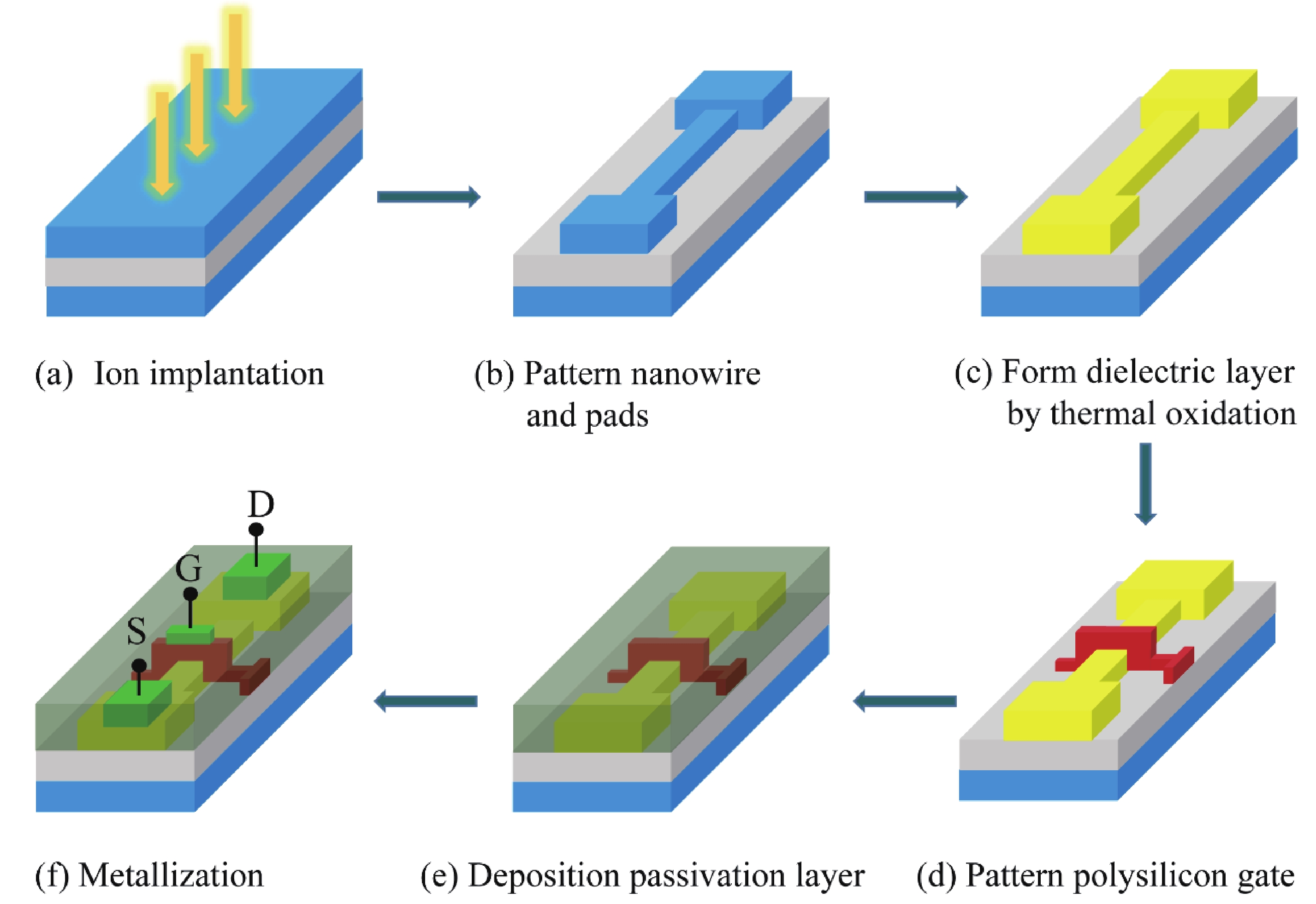
    Fig. 1. (Color online) Schematic diagrams of the fabrication process for JNTs.
    (Color online) (a) The color SEM image of devices with the gate length of 280 nm. (b) The cross-section schematics of the devices.
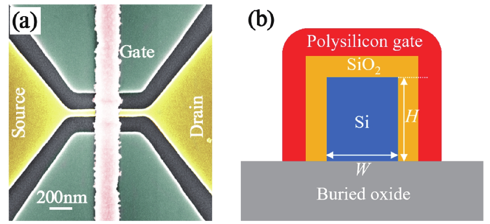
    Fig. 2. (Color online) (a) The color SEM image of devices with the gate length of 280 nm. (b) The cross-section schematics of the devices.
    (Color online) Measured drain current characteristics at room temperature, showing (a) drain current versus gate voltage for drain voltages of 0.1 to 4.1 V with step of 1 V, and (b) drain current versus drain voltage for gate voltages from 1 to 4 V with step of 1 V.
    Fig. 3. (Color online) Measured drain current characteristics at room temperature, showing (a) drain current versus gate voltage for drain voltages of 0.1 to 4.1 V with step of 1 V, and (b) drain current versus drain voltage for gate voltages from 1 to 4 V with step of 1 V.
    (Color online) (a) IDS–VDS output characteristics of JNT device at T = 10 K. (b) The transfer characteristics of the JNT with VGS sweep from 0 to 3.5 V and back.
    Fig. 4. (Color online) (a) IDSVDS output characteristics of JNT device at T = 10 K. (b) The transfer characteristics of the JNT with VGS sweep from 0 to 3.5 V and back.
    (Color online) (a) IDS–VGS curves for VDS values ranging from 2 to 10 mV in steps of 2 mV. The detail image in the upper left corner is an enlarged detail. (b) Time domain current levels versus time trace at VGS = 2.2 V and VDS = 10 mV.
    Fig. 5. (Color online) (a) IDSVGS curves for VDS values ranging from 2 to 10 mV in steps of 2 mV. The detail image in the upper left corner is an enlarged detail. (b) Time domain current levels versus time trace at VGS = 2.2 V and VDS = 10 mV.
    (Color online) ln(τc/τe) and its linear fitting. The slope is proportional to xT, the position of the traps in the oxide.
    Fig. 6. (Color online) ln(τc/τe) and its linear fitting. The slope is proportional to xT, the position of the traps in the oxide.
    (Color online) (a) Transfer characteristics at the temperatures of 100 to 300 K with the step of 50 K. (b) Measured VTH and SS at VDS = 0.1 V versus temperature. The black dashed line represents the theoretical value of subthreshold swing SStheo.
    Fig. 7. (Color online) (a) Transfer characteristics at the temperatures of 100 to 300 K with the step of 50 K. (b) Measured VTH and SS at VDS = 0.1 V versus temperature. The black dashed line represents the theoretical value of subthreshold swing SStheo.
    (Color online) (a) Simulated IDS–VGS curves for different trap densities with the trap level equals to the intrinsic Fermi level. (b) Threshold voltage as a function of trap densities with different trap levels.
    Fig. 8. (Color online) (a) Simulated IDSVGS curves for different trap densities with the trap level equals to the intrinsic Fermi level. (b) Threshold voltage as a function of trap densities with different trap levels.
    Yifan Fu, Liuhong Ma, Zhiyong Duan, Weihua Han. Effect of charge trapping on electrical characteristics of silicon junctionless nanowire transistor[J]. Journal of Semiconductors, 2022, 43(5): 054101
    Download Citation