
Yifan Fu, Liuhong Ma, Zhiyong Duan, Weihua Han. Effect of charge trapping on electrical characteristics of silicon junctionless nanowire transistor[J]. Journal of Semiconductors, 2022, 43(5): 054101
- Journal of Semiconductors
- Vol. 43, Issue 5, 054101 (2022)
Abstract
1. Introduction
Rapid downscaling of metal-oxide-semiconductor field-effect transistors (MOSFETs) causes many adverse issues, such as short channel effects (SCEs) and carrier mobility degradation, which will seriously affect the performance of related devices. More seriously, as the size of MOSFETs continues to shrink to the nanometer scale, the fabrication process for the source/drain of the traditional inversion mode transistor is facing more challenges. In recent years, several novel materials have been proposed to keep up with the pace of Moore’s law, such as two-dimensional (2D) semiconductor materials[
The key to the fabrication of JNTs is that the channel must be thin enough to ensure that the device is turned off at zero gate voltage. In addition, due to the excellent electrostatic controllability, the tri-gate structure is undoubtedly the best choice for JNT manufacture. Interface traps will be inevitably formed in the process of transistor fabrication, which will directly affect the electrical characteristics and reliability of devices[
In this paper, we fabricated tri-gate JNTs through experiments, and investigated the electrical properties of the fabricated devices at different temperatures. At low temperatures, we observed irregular current protrusions. This is a phenomenon caused by interface traps. We analyzed the influence of interface traps on the electrical characteristics of JNT by adding interface traps with different densities and different energy levels to a three-dimension (3D) model built by COMSOL Multiphysics simulation software[
2. Experimental methods
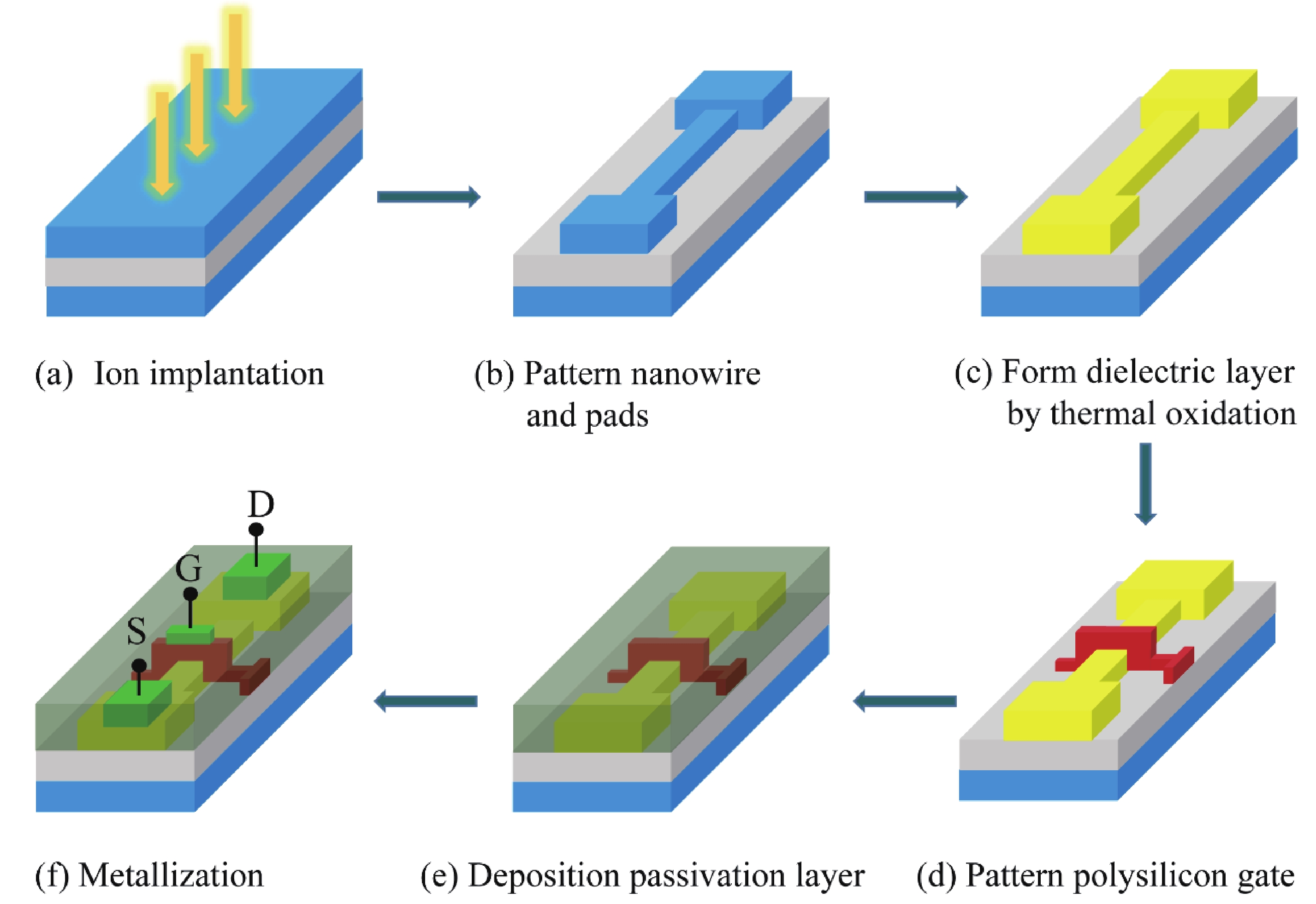
Fig. 1 shows the schematic diagrams of the fabrication process of JNTs. The devices were fabricated on a silicon-on-insulator (SOI) substrate with the top silicon layer of 55 nm. The SOI wafer was uniformly and heavily doped by phosphorus ion implantation with a dose of 5 × 1013 cm–2 (Fig. 1(a)). And then electron beam lithography (EBL) and inductively coupled plasma (ICP) etching were performed to define the active region and the channel fin (Fig. 1(b)). It was followed by a sacrificial oxidation to eliminate the etching induced surface damage and then 22-nm-thick gate oxide was grown at 900 °C in dry oxygen for 1 h (Fig. 1(c)). Then, a 150-nm-thick boron doped polysilicon gate was defined, wrapped around three sides of the silicon channel (Fig. 1(d)). The poly-silicon was then doped by arsenic ion implantation at a dose of 1 × 1020 cm–3 after annealing at 1000 °C for 10 s. After depositing 200-nm-thick silicon dioxide as the protective layer, ohmic contact windows were opened (Fig. 1(e)). Following 400-nm-thick aluminum was evaporated and lifted off as final metallization via conventional optical lithography (Fig. 1(f)). The cross-section schematics and the scanning electron microscope (SEM) image of the tri-gate JNT are shown in Fig. 2. The final cross section of the silicon core was estimated to be 30 nm in height (H) and 30 nm in width (W), respectively. The length of polysilicon gate (Lg) was 280 nm. For the low temperature electrical characterization, the devices were measured in a vacuum chamber, which can be cooled down to 10 K. The conventional operation of JNTs is to apply a positive gate voltage to create an electroneutral region in the channel region and allow electrons to flow.
![]()
Figure 1.(Color online) Schematic diagrams of the fabrication process for JNTs.
![]()
Figure 2.(Color online) (a) The color SEM image of devices with the gate length of 280 nm. (b) The cross-section schematics of the devices.
3. Results and discussion
Firstly, we tested the relevant electrical characteristics of the devices at room temperature. Fig. 3(a) shows the transfer characteristic curves. The drain voltage VDS is set to be 0.1 to 4.1 V with the step of 1 V. As the gate voltage VGS continues to increase, the drain current IDS also increases, gradually reaching a saturated state. The subthreshold swing (SS) and the threshold voltage (VTH) are 132 mV/dec and 0.26 V, respectively. The curves of drain current IDS versus VGS show that the fabricated JNT operates as a normally-off device with a low gate leakage current of several pA and the on/off current ratio larger than 1 × 10⁴. Besides, the output curves in Fig. 3(b) demonstrate excellent gate control ability in our devices.
![]()
Figure 3.(Color online) Measured drain current characteristics at room temperature, showing (a) drain current versus gate voltage for drain voltages of 0.1 to 4.1 V with step of 1 V, and (b) drain current versus drain voltage for gate voltages from 1 to 4 V with step of 1 V.
The temperature-dependent electrical properties of JNT were carried out by Lakershore-340 temperature controller under vacuum environment. Fig. 4(a) shows the output characteristics of JNT measured at the temperature of 10 K. Obvious current jumps are observed at some special values of VGS such as 2.20 V. Besides, the current jumps increase with the increase of the absolute value of the bias, indicating the existence of active traps[
![]()
Figure 4.(Color online) (a)
Fig. 5(a) shows the transfer characteristic curve of this device at a low temperature of 10 K. The drain voltage is set to be 2–10 mV with the step of 2 mV. Obvious current jumps are observed around the gate bias of roughly 2.2 V, at which voltage, the trap level and the silicon channel Fermi level move close to each other so that hopping and tunneling happen. The trap is found to be an acceptor type center[
![]()
Figure 5.(Color online) (a)
where tox is the oxide thickness, k is Boltzmann constant and q is the elementary charge. Through linear fitting of VGS dependence of ln(τc/τe) as shown in Fig. 6, the accurate vertical trap depth obtained by Eq. (1) is 0.35 nm. Compared to the oxide thickness of 22 nm, these traps can be considered as interface traps.
![]()
Figure 6.(Color online) ln(
In Fig. 7(a), the measured IDS as a function of the VGS with the device biased at a drain voltage of VDS = 0.1 V is presented for different temperatures. It can be noted that the drain current decreases with temperature. The threshold voltage VTH and subthreshold swing SS are presented as a function of the temperatures in Fig. 7(b). The slope of VTH varied with the temperatures is an approach to –4.23 mV/K and the slope of SS is 0.58 mV/dec/K. It should be noted that the SS variation with temperatures of our JNT device is larger than that of the theoretical value. We attribute this phenomenon to the influence of interface traps. The subthreshold swing SS depending on the trap density Ntrap is described by[
![]()
Figure 7.(Color online) (a) Transfer characteristics at the temperatures of 100 to 300 K with the step of 50 K. (b) Measured
where Cox is the gate oxide capacitance per unit area (estimated to be 1.56 × 10⁻⁷ F/cm2). The presence of interface traps will deteriorate the subthreshold characteristics. The interface trap density obtained from Eq. (2) is approximately to be 1.9 × 1012 cm–2.
To further investigate the influence of interface traps on JNT electrical characteristics, we construct a 3D tri-gate JNT structure in COMSOL Multiphysics simulation software with the Semiconductor Module. The parameters of the simulation device are consistent with the experimental device. The gate with a 22-nm-thick oxide layer and surface traps is modeled using the thin insulator gate boundary condition around the perimeter of the channel. The drain and source boundaries are ideal ohmic contacts, and the voltages are set to ground and 0.1 V, respectively. The gate voltage is swept from 0 to 8 V for different surface trap densities. The simulated device structure is shown in the insert of Fig. 8(a). Here, Ls and Ld are the distances of the source and the drain from the channel region, respectively. Those two parameters are set to 200 nm. At first, the influence of trap density on the transfer characteristic is investigated. The simulated curves are shown in Fig. 8(a). The transfer curves are positively shifted with increasing interface trap density. Besides, the influence of the trap levels is also investigated in Fig. 8(b). Here the energy difference between the trap energy level Et and the intrinsic Fermi level Ei is set as –0.18, –0.04 , 0, 0.06 and 0.24 eV, respectively. For the same trap density, the threshold voltage will shift positively as the trap level moves away from the conduction band. Therefore, combining the experimental data with the simulation results, we obtain that the position of trap level is 0.18 eV below the intrinsic Fermi level, and the trap density is 1.9 × 1012 cm–2.
![]()
Figure 8.(Color online) (a) Simulated
4. Conclusion
In summary, we fabricated junctionless tri-gate nanowire transistors on the SOI substrate. We analyzed the electrical properties of the manufactured devices at different temperatures (10–300 K). Obvious RTS were observed at low temperature of 10 K. This phenomenon indicates that there are acceptor-like trap states in the devices. Through linear fitting of gate voltage dependence of ln(τc/τe), the accurate vertical trap depth of 0.35 nm is obtained. Thus, the acceptor-like traps can be considered as interface traps. Besides, from the slope of the subthreshold swing versus temperature, we estimate the interface trap density to be 1.9 × 1012 cm–2. In addition, we use COMSOL Multiphysics simulation software to build a 3D model for the device. In the model, traps with different densities and different energy levels are added to the interface between the conductive channel and the gate dielectric layer. According to the simulation results of threshold voltage, we estimate that the energy level of the interface traps is located at 0.18 eV below the intrinsic Fermi level. The results provide a theoretical guidance for analyzing the effects of interface traps on the junctionless transistors.
Acknowledgements
This work is supported by the National Natural Science Foundation of China (Grant Nos. 613760966, 1327813, 61404126 and 11947115), the Natural Science Foundation of Henan Province under (Grant No. 202300410444), and Foreign Experts Program of Ministry of Science and Technology in China (Grant No. G2021026027L).
References
[1] W H Zhou, S L Zhang, S Y Guo et al. Designing sub-10-nm metal-oxide-semiconductor field-effect transistors via ballistic transport and disparate effective mass: The case of two-dimensional BiN. Phys Rev Appl, 13, 044066(2020).
[2] W H Zhou, S L Zhang, Y Y Wang. Anisotropic in-plane ballistic transport in monolayer black arsenic-phosphorus FETs. Adv Electron Mater, 6, 1901281(2020).
[3] D Y Jeon, M Mouis, S Barraud et al. Channel width dependent subthreshold operation of tri-gate junctionless transistors. Solid-State Electron, 171, 107860(2020).
[4] J P Colinge, C W Lee, A Afzalian et al. Nanowire transistors without junctions. Nat Nanotechnol, 5, 225(2010).
[5] N Mendiratta, S L Tripathi. A review on performance comparison of advanced MOSFET structures below 45 nm technology node. J Semicond, 41, 061401(2020).
[6] J Lee, Y Kim, S Cho. Design of poly-Si junctionless Fin-channel FET with quantum-mechanical drift-diffusion models for sub-10-nm technology nodes. IEEE Trans Electron Dev, 63, 4610(2016).
[7] R Yan, A Kranti, I Ferain et al. Investigation of high-performance sub-50 nm junctionless nanowire transistors. Microelectron Reliab, 51, 1166(2011).
[8] T Rudenko, A Nazarov, I Ferain et al. Mobility enhancement effect in heavily doped junctionless nanowire silicon-on-insulator metal-oxide-semiconductor field-effect transistors. Appl Phys Lett, 101, 053511(2012).
[9] S Gupta, K Nigam, S Pandey et al. Effect of interface trap charges on performance variation of heterogeneous gate dielectric junctionless-TFET. IEEE Trans Electron Dev, 64, 1(2017).
[10] A N Nazarov, I Ferain, N D Akhavan et al. Random telegraph-signal noise in junctionless transistors. Appl Phys Lett, 98, 092111(2011).
[11] O M Berengue, J Chiquito. Direct evidence of traps controlling the carriers transport in SnO2 nanobelts. J Semicond, 38, 122001(2017).
[12] L H Ma, W H Han, H Wang et al. Charge trapping in surface accumulation layer of heavily doped junctionless nanowire transistors. Chin Phys B, 024, 589(2015).
[13] G X Hu, S Y Hu, J H Feng et al. Analytical models for channel potential, threshold voltage, and subthreshold swing of junctionless triple-gate FinFETs. Microelectron J, 50, 60(2016).
[14] F Y Liu, H Z Liu, B W Liu et al. An analytical model for nanowire junctionless SOI FinFETs with considering three-dimensional coupling effect. Chin Phys B, 25, 047305(2016).
[15] F Ávila-Herreraa, B C Pazb, A Cerdeira. Charge-based compact analytical model for triple-gate junctionless nanowire transistors. Solid-State Electron, 122, 23(2016).
[16] Y Y Liang, Kyungsoo Jang, S Velumani et al. Effects of interface trap density on the electrical performance of amorphous InSnZnO thin-film transistor. J Semicond, 36, 024007(2015).
[17] F Liu, K L Wang, C Li et al. Study of random telegraph signals in single-walled carbon nanotube field effect transistors. IEEE Trans Nanotechnol, 5, 441(2006).
[18] Y Sun, L N Zhang, Z Ahmed et al. Characterization of interface trap dynamics responsible for hysteresis in organic thin-film transistors. Org Electron, 27, 192(2015).
[19] N V Amarasinghe, Z Elik-Butler, P Vasina et al. Characterization of oxide traps in 0.15 μm2 MOSFETs using random telegraph signals. Microelectron Reliab, 40, 1875(2000).
[20] Z Celik-Butler, P Vasina. A method for locating the position of oxide traps responsible for random telegraph signals in submicron MOSFETs. IEEE Trans Electron Dev, 47, 646(2000).
[21] Y C Cheng, H B Chen, M H Han et al. Temperature dependence of electronic behaviors in quantum dimension junctionless thin-film transistor. Nanoscale Res Lett, 9, 1(2014).

Set citation alerts for the article
Please enter your email address
© Copyright 2018-2021 | Chinese Laser Press. All Rights Reserved 沪ICP备15018463号-20