• Journal of Semiconductors
  • Vol. 41, Issue 7, 072904 (2020)
Fuyou Liao1、4, Hongjuan Wang2、3, Xiaojiao Guo1, Zhongxun Guo1, Ling Tong1, Antoine Riaud1, Yaochen Sheng1, Lin Chen1, Qingqing Sun1, Peng Zhou1, David Wei Zhang1, Yang Chai4、5, Xiangwei Jiang3, Yan Liu2, and Wenzhong Bao1
Author Affiliations
  • 1State Key Laboratory of ASIC and System, School of Microelectronics, Fudan University, Shanghai 200433, China
  • 2State Key Discipline Laboratory of Wide Bandgap Semiconductor Technology, School of Microelectronics, Xidian University, Xi'an 710071, China
  • 3Institute of Semiconductors, Chinese Academy of Sciences, Beijing 100083, China
  • 4The Hong Kong Polytechnic University Shenzhen Research Institute, Shenzhen 518057, China
  • 5Department of Applied Physics, The Hong Kong Polytechnic University, Hong Kong, China
  • show less
    DOI: 10.1088/1674-4926/41/7/072904 Cite this Article
    Fuyou Liao, Hongjuan Wang, Xiaojiao Guo, Zhongxun Guo, Ling Tong, Antoine Riaud, Yaochen Sheng, Lin Chen, Qingqing Sun, Peng Zhou, David Wei Zhang, Yang Chai, Xiangwei Jiang, Yan Liu, Wenzhong Bao. Charge transport and quantum confinement in MoS2 dual-gated transistors[J]. Journal of Semiconductors, 2020, 41(7): 072904 Copy Citation Text show less
    (Color online) (a) Side-view schematic illustration of a MoS2 DG-FET. (b) Optical microscopic image of an exfoliated MoS2 sheet on a 200-nm-thick Al2O3 substrate. (c) Raman spectra of MoS2 sheets with thickness ranging from 1L to 4L. (d) Optical image of a typical 4-terminal device, the top gate electrode is relatively thin (15 nm) but still conductive. The lower graph is a schematic of the 4-terminal device in which W is the channel width and L is the distance between two inner pads. V1 and V2 are used to gauge the voltage drop between two inner contacts.
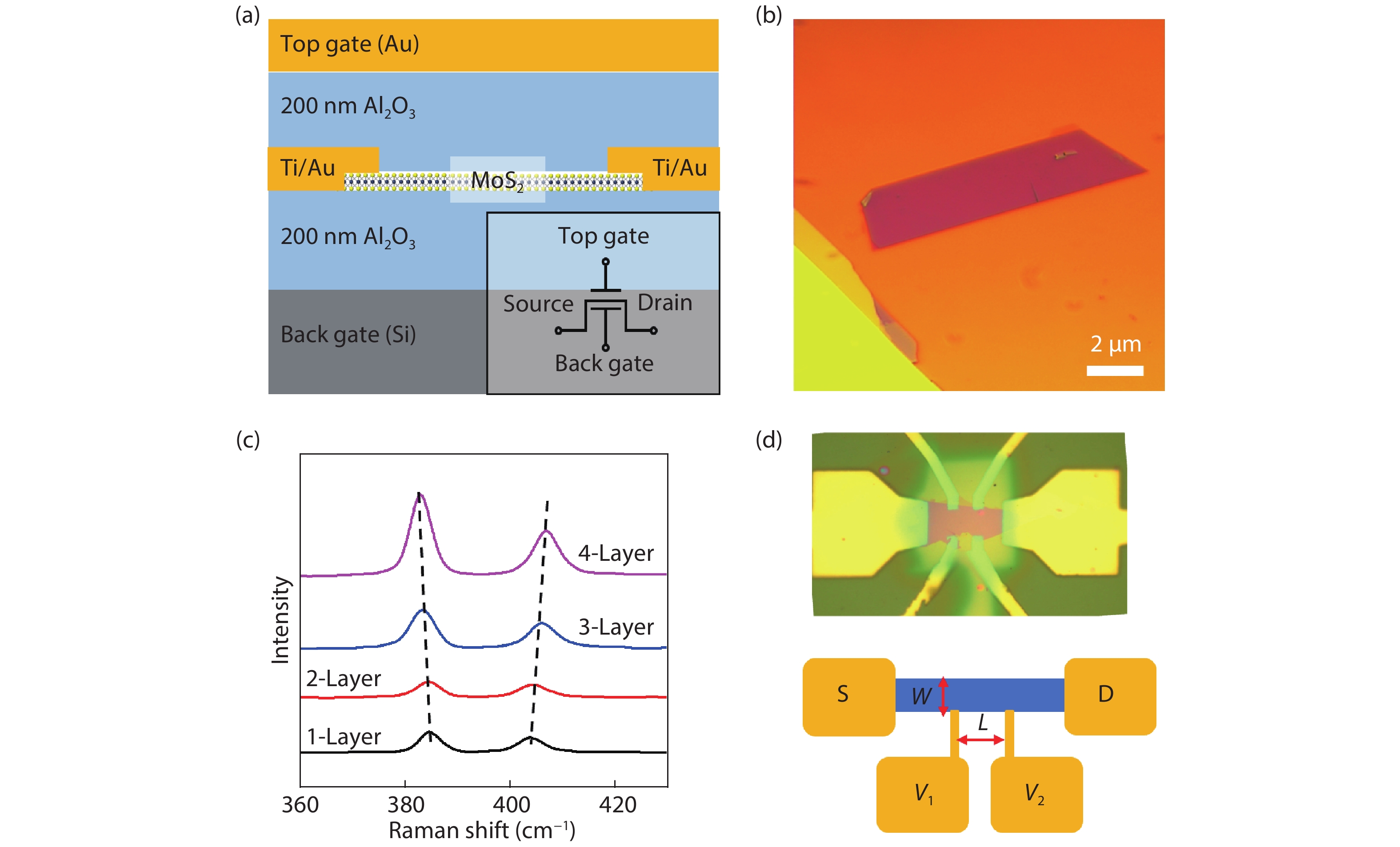
    Fig. 1. (Color online) (a) Side-view schematic illustration of a MoS2 DG-FET. (b) Optical microscopic image of an exfoliated MoS2 sheet on a 200-nm-thick Al2O3 substrate. (c) Raman spectra of MoS2 sheets with thickness ranging from 1L to 4L. (d) Optical image of a typical 4-terminal device, the top gate electrode is relatively thin (15 nm) but still conductive. The lower graph is a schematic of the 4-terminal device in which W is the channel width and L is the distance between two inner pads. V1 and V2 are used to gauge the voltage drop between two inner contacts.
    (Color online) (a) Four-terminal conductivity σ4prob as functions of BG, TG and DG voltages. Solid and dashed curves correspond to linear and logarithmic coordinates, respectively. (b) 2D contour plot of σ4prob as functions of VBG and VTG at room temperature. (c) Mobility versus sheet thickness collected from 10 MoS2 DG-FETs work under DG mode.
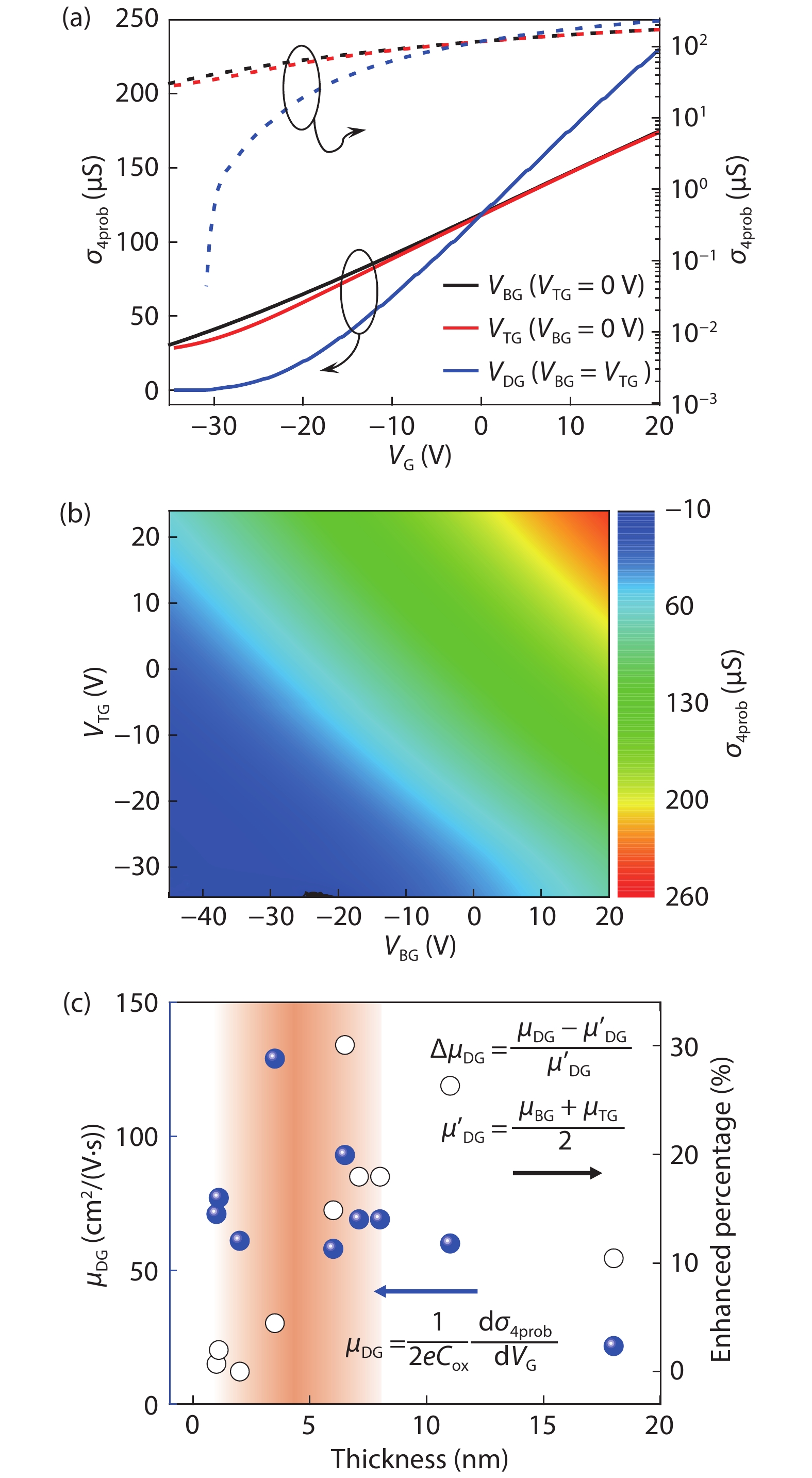
    Fig. 2. (Color online) (a) Four-terminal conductivity σ4prob as functions of BG, TG and DG voltages. Solid and dashed curves correspond to linear and logarithmic coordinates, respectively. (b) 2D contour plot of σ4prob as functions of VBG and VTG at room temperature. (c) Mobility versus sheet thickness collected from 10 MoS2 DG-FETs work under DG mode.
    (Color online) (a) With and (b) without considering quantum confinement effect, the simulation results of carrier redistribution of a 2-nm-thick MoS2. The upper and lower panels show the simulation results from the SG (VBG= 10 V) and DG (VBG= VTG= 10 V) device, respectively. (c) The electron density in the channel of the DG MoS2 device versus channel thickness. The dielectric layer is 200 nm Al2O3. for all devices
    Fig. 3. (Color online) (a) With and (b) without considering quantum confinement effect, the simulation results of carrier redistribution of a 2-nm-thick MoS2. The upper and lower panels show the simulation results from the SG (VBG= 10 V) and DG (VBG= VTG= 10 V) device, respectively. (c) The electron density in the channel of the DG MoS2 device versus channel thickness. The dielectric layer is 200 nm Al2O3. for all devices
    (Color online) Temperature dependence electrical measurement. (a) The temperature-dependent σ as a function of VDG of a four-probe device. MoS2 is ~5 nm thick with 200 nm Al2O3 of both TG and BG dielectrics. (b) The temperature-dependent mobility extracted from monolayer MoS2 (black dot) and multi-layer MoS2 DG-FET (red square). Monolayer MoS2 DG-FET is 15 nm HfO2 of both TG and BG dielectrics.
    Fig. 4. (Color online) Temperature dependence electrical measurement. (a) The temperature-dependent σ as a function of VDG of a four-probe device. MoS2 is ~5 nm thick with 200 nm Al2O3 of both TG and BG dielectrics. (b) The temperature-dependent mobility extracted from monolayer MoS2 (black dot) and multi-layer MoS2 DG-FET (red square). Monolayer MoS2 DG-FET is 15 nm HfO2 of both TG and BG dielectrics.
    Fuyou Liao, Hongjuan Wang, Xiaojiao Guo, Zhongxun Guo, Ling Tong, Antoine Riaud, Yaochen Sheng, Lin Chen, Qingqing Sun, Peng Zhou, David Wei Zhang, Yang Chai, Xiangwei Jiang, Yan Liu, Wenzhong Bao. Charge transport and quantum confinement in MoS2 dual-gated transistors[J]. Journal of Semiconductors, 2020, 41(7): 072904
    Download Citation