
Fuyou Liao, Hongjuan Wang, Xiaojiao Guo, Zhongxun Guo, Ling Tong, Antoine Riaud, Yaochen Sheng, Lin Chen, Qingqing Sun, Peng Zhou, David Wei Zhang, Yang Chai, Xiangwei Jiang, Yan Liu, Wenzhong Bao. Charge transport and quantum confinement in MoS2 dual-gated transistors[J]. Journal of Semiconductors, 2020, 41(7): 072904
- Journal of Semiconductors
- Vol. 41, Issue 7, 072904 (2020)
Abstract
1. Introduction
Atomic thick two-dimensional (2D) layered materials, such as semi-metallic graphene and semiconductive transition metal dichalcogenides (TMDCs), have emerged as an attractive candidate for future electronic and optoelectrical materials[
Since the bandgap size is dependent on the MoS2 layer number[
Here, we successfully fabricate the MoS2 DG-FETs with symmetric back gate (BG) and top gate (TG) based on monolayer and multilayer MoS2 films. The thickness-dependent charge transport in our MoS2 DG structure is revealed by a four-probe electrical measurement which excludes the contact influence, and TCAD simulation shows that the impact of quantum confinement effect exists in thin MoS2 sheet sandwiched by the DG. Such effect attenuates with larger thickness, but still exist in a 5-nm-thick channel. The temperature-dependent electrical measurement of our device also indicates that transport of multilayer MoS2 DG-FET is in the phonon-limited transport regime, while single layer MoS2 device shows typical Coulomb impurity (CI) limited regime.
2. Device structure and material characterization
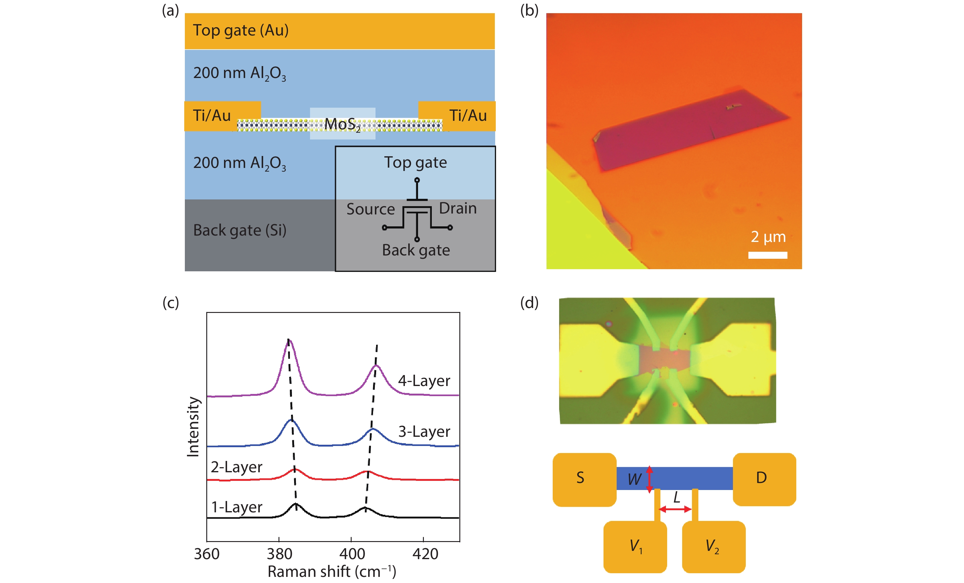
The cross-sectional schematic of MoS2 DG-FET is depicted in Fig. 1(a). The fabrication process for such devices starts from the deposition of a 200-nm-thick Al2O3 layer by atom layer deposition (ALD, MNT-100-4) on a heavily doped Si substrate, which acts as a BG dielectric layer. Then multilayer MoS2 flakes are mechanically exfoliated on top of Al2O3, and a typical optical microscopic image is shown in Fig. 1(b). Uniform and rectangular shaped MoS2 sheets are selected for subsequent device fabrication. Raman characterization (laser excitation wavelength of 514 nm) is then carried out to confirm the layer number and crystalline quality, as shown in Fig. 1(c). To avoid lithography contamination, electrical contacts (5 nm Ti/30 nm Au) are patterned using a stencil mask technique[
![]()
Figure 1.(Color online) (a) Side-view schematic illustration of a MoS2 DG-FET. (b) Optical microscopic image of an exfoliated MoS2 sheet on a 200-nm-thick Al2O3 substrate. (c) Raman spectra of MoS2 sheets with thickness ranging from 1L to 4L. (d) Optical image of a typical 4-terminal device, the top gate electrode is relatively thin (15 nm) but still conductive. The lower graph is a schematic of the 4-terminal device in which
The field-effect mobility μ is a crucial factor to characterize the FET performance. For most TMDCs-based FETs, the effective value of μ is mainly governed by the contact rather than the channel itself[
3. Experimental result and discussion
The measured σ4prob as functions of BG, TG and DG modes are shown in Fig. 2(a). It is noted that results from BG and TG modes are highly coincident due to their symmetric gating capability, while a weak mismatch at negative gate voltage region can also be observed, which may result from their different dielectric-MoS2 interfaces. As for the BG, MoS2 is directly transferred on to the pre-deposited Al2O3, while for the TG, the interface quality degrades because of the absence of dangling bonds on MoS2 for deposition of Al2O3.
![]()
Figure 2.(Color online) (a) Four-terminal conductivity
It also shows that DG mode displays an improved channel electrostatic control than that of BG or TG. To further illustrate the gate modulation by BG and TG, a 2D contour plot of σ4prob as functions of VBG and VTG is then plotted in Fig. 2(b). Such 2D diagram shows parallel diagonal contours with constant current, and the slope of these contours line is approximately 1, indicating that the BG and TG exhibit the same capability to modulate the channel, since the oxidation layer capacitance of the back gate and top gate is nearly symmetrical (CBG /CTG ≈ 1).
For SG structure, the field-effect (FE) mobility can be estimated by
Depending on the channel thickness, there is a competition of multiple mechanisms in our MoS2 DG-FETs: 1) larger current carrying ability in thicker channels, but with considerable interlayer resistance[
To ravel the impact from quantum confinement effect, the carrier density, and distribution of the DG-FETs are then simulated by using the van Dort model, the 1D Schrödinger equation, the density gradient model, and the modified local-density approximation (MLDA). The van Dort model computes the impact of electric field normal to the channel interface on the carrier density modification due to the quantization. Based on the energy band structures in the channel, the 1D Schrödinger equation was solved self-consistently with the Poisson equation. The eigenvalues and wave functions for electrons and holes were obtained with consideration of multi valleys in conduction and valence bands. The density gradient model added the quantum correction to the carrier distribution at interfaces in the device by introducing the reciprocal thermal energy, mass-driving term, and the smoothed potential[
Figs. 3(a) and 3(b) compare the quantum-confinement impact on the simulated carrier redistribution in SG (VBG = 10 V) and DG (VBG = VTG = 10 V) structures. In the DG structure, quantum confinement effect is rather prominent, it repulses carriers away from dielectric-MoS2 interfaces and confines carriers inside the channel, which can suppress phonon and Coulomb scattering at interfaces and contribute to the mobility improvement. On the opposite, the carriers in the SG structure are pushed towards one side of MoS2, amplifying the interface scattering. Fig. 3(c) shows the calculated carrier distribution in MoS2 DG device with a series of channel thicknesses, by considering quantum confinement effect. It is noticed that the impact of quantum confinement effect attenuates with larger thickness but still exist in a 5 nm thick channel.
![]()
Figure 3.(Color online) (a) With and (b) without considering quantum confinement effect, the simulation results of carrier redistribution of a 2-nm-thick MoS2. The upper and lower panels show the simulation results from the SG (
Thus, a complete scenario for thickness dependence of MoS2 DG-FET can be: thicker MoS2 carries current larger but with less quantum confinement effect, and there are also trade-offs including large interlayer resistance and screening effect than weakens the gate control. For practical applications of MoS2 FETs, considering critical parameters including μ, SS and current on/off ratio, a layer thickness in the range of 2–6 nm would be ideal by achieving overall satisfying μ, SS and current on/off ratio[
We then investigate the temperature-dependent electrical properties of our MoS2 DG-FETs. Fig. 4(a) shows the temperature-dependent transfer curve from a multilayer MoS2 device (~ 5 nm). The channel current increases when temperature decreases, while the threshold voltage VTH hardly shifts when lowering the temperature. In the 4-terminal device architecture, mobility extraction is more accurate, as shown in Fig. 4(b). The mobility in a multi-layer MoS2 DG-FET is as high as 763 cm2/(V·s) (n ≈ 1013 cm–2) at 125 K (plotted by red point) and can be fitted by T–γ for T > 100 K with γ = 2.5, which is in good agreement with theoretically predicted value (γ between 1.52 and 2.6)[
![]()
Figure 4.(Color online) Temperature dependence electrical measurement. (a) The temperature-dependent σ as a function of
4. Conclusion
We reported a systematic investigation of carrier transport in MoS2 DG-FETs with a variation of MoS2 channel thickness. DG structure provides better electrostatic control for the MoS2 FETs. Moreover, quantum confinement plays an important role in the charge transport, as for a certain thickness of MoS2, confinement of the charge in the center of the channel under DG mode reduces the scattering and thus boosts the mobility compared to single gating of a similar thickness layer. The TCAD simulation considering quantum confinement reveals that the impact of quantum confinement effect attenuates with larger thickness but still exist in a 5 nm thick channel. Furthermore, the phonon-limited transport regime and CI limited regime were revealed in multi-layer MoS2 DG-FETs and single layer MoS2 by temperature-dependent transfer curves, respectively. Such device architecture together with similar results can be extended to other TMDCs based devices.
Acknowledgements
This work was supported by the National Key Research and Development Program of China (2016YFA0203900, 2018YFA0306101), the National Natural Science Foundation of China (Grant No. 91964202), and Shanghai Municipal Science and Technology Commission (18JC1410300).
References
[1] K S Novoselov, A K Geim, S V Morozov et al. Electric field effect in atomically thin carbon films. Science, 306, 666(2004).
[2] B Radisavljevic, A Radenovic, J Brivio et al. Single-layer MoS2 transistors. Nat Nanotechnol, 6, 147(2011).
[3] Q H Wang, K Kalantar-Zadeh, A Kis et al. Electronics and optoelectronics of two-dimensional transition metal dichalcogenides. Nat Nanotechnol, 7, 699(2012).
[4] G Wu, X Wang, Y Chen et al. MoTe2 p–n homojunctions defined by ferroelectric polarization. Adv Mater, 32, 1907937(2020).
[5] L Tu, R Cao, X Wang et al. Ultrasensitive negative capacitance phototransistors. Nat Commun, 11, 101(2020).
[6] G Wu, B Tian, L Liu et al. Programmable transition metal dichalcogenide homojunctions controlled by nonvolatile ferroelectric domains. Nat Electron, 3, 43(2020).
[7] S B Desai, S R Madhvapathy, A B Sachid et al. MoS2 transistors with 1-nanometer gate lengths. Science, 354, 99(2016).
[8] F Ahmed, M S Choi, X Liu et al. Carrier transport at the metal-MoS2 interface. Nanoscale, 7, 9222(2015).
[9] B W Baugher, H O Churchill, Y Yang et al. Intrinsic electronic transport properties of high-quality monolayer and bilayer MoS2. Nano Lett, 13, 4212(2013).
[10]
[11] H Liu, A T Neal, P D Ye. Channel length scaling of MoS2 MOSFETs. ACS Nano, 6, 8563(2012).
[12] C Lee, H Yan, L E Brus et al. Anomalous lattice vibrations of single- and few-layer MoS2. ACS Nano, 4, 2695(2010).
[13] K F Mak, C Lee, J Hone et al. Atomically thin MoS2: A new direct-gap semiconductor. Phys Rev Lett, 105, 136805(2010).
[14] S W Han, H Kwon, S K Kim et al. Band-gap transition induced by interlayer van der Waals interaction in MoS2. Phys Rev B, 84, S312(2011).
[15] P Bolshakov, A Khosravi, P Zhao et al. Dual-gate MoS2 transistors with sub-10 nm top-gate high-
[16] X Zou, J Xu, H Huang et al. A comparative study on top-gated and bottom-gated multilayer MoS2 transistors with gate stacked dielectric of Al2O3/HfO2. Nanotechnology, 29, 245201(2018).
[17] A Nourbakhsh, A Zubair, S Huang et al. 15-nm channel length MoS2 FETs with single-and double-gate structures. 2015 Symposium on VLSI Technology (VLSI Technology), T28(2015).
[18] G H Lee, X Cui, Y D Kim et al. Highly stable, dual-gated MoS2 transistors encapsulated by hexagonal boron nitride with gate-controllable contact, resistance, and threshold voltage. ACS Nano, 9, 7019(2015).
[19] H Liu, P D Ye. MoS2 dual-gate MOSFET with atomic-layer-deposited Al2O3 as top-gate dielectric. IEEE Electron Device Lett, 33, 546(2012).
[20] F Liao, J Deng, X Chen et al. A dual-gate MoS2 photodetector based on interface coupling effect. Small, 16, 1904369(2020).
[21] F Liao, Z Guo, Y Wang et al. High-performance logic and memory devices based on a dual-gated MoS2 architecture. ACS Appl Electron Mater, 2, 111(2020).
[22] F Liao, Y Sheng, Z Guo et al. MoS2 dual-gate transistors with electrostatically doped contacts. Nano Res, 12, 2515(2019).
[23] W Bao, G Liu, Z Zhao et al. Lithography-free fabrication of high quality substrate-supported and freestanding graphene devices. Nano Res, 3, 98(2010).
[24] S Das, H Y Chen, A V Penumatcha et al. High performance multilayer MoS2 transistors with scandium contacts. Nano Lett, 13, 100(2013).
[25] Y Liu, J Guo, E Zhu et al. Approaching the Schottky–Mott limit in van der Waals metal –semiconductor junctions. Nature, 557, 696(2018).
[26] W Bao, X Cai, D Kim et al. High mobility ambipolar MoS2 field-effect transistors: Substrate and dielectric effects. Appl Phys Lett, 102, 042104(2012).
[27] M W Lin, I I Kravchenko, J Fowlkes et al. Thickness-dependent charge transport in few-layer MoS2 field-effect transistors. Nanotechnology, 27, 165203(2016).
[28] M G Anconaand, G J Iafrate. Quantum correction to the equation of state of an electron gas in a semiconductor. Phys Rev B, 39, 9536(1989).
[29] K Uchida, J Koga, S Takagib. Experimental study on electron mobility in ultrathin-body silicon-on-insulator metal–oxide–semiconductor field-effect transistors. J Appl Phys, 102, 074510(2007).
[30] R Fivaz, E Mooser. Mobility of charge carriers in semiconducting layer structures. Phys Rev, 163, 743(1967).
[31] K Kaasbjerg, K S Thygesen, K W Jacobsen. Phonon-limited mobility in n-type single-layer MoS2 from first principles. Phys Rev B, 85, 115317(2012).
[32] N Ma, D Jena. Charge scattering and mobility in atomically thin semiconductors. Phys Rev X, 4, 011043(2014).
[33] Z Y Ong, M V Fischetti. Mobility enhancement and temperature dependence in top-gated single-layer MoS2. Physics, 88, 1653(2013).

Set citation alerts for the article
Please enter your email address
© Copyright 2018-2021 | Chinese Laser Press. All Rights Reserved 沪ICP备15018463号-20