
Guiping Cao, Ning Dong. An 18-bit sigma –delta switched-capacitor modulator using 4-order single-loop CIFB architecture[J]. Journal of Semiconductors, 2020, 41(6): 062404
- Journal of Semiconductors
- Vol. 41, Issue 6, 062404 (2020)
Abstract
1. Introduction
The idea of sigma–delta (Σ–Δ) modulation was first proposed in 1962 by Inoise et al.[
Structurally, the Σ–Δ ADC is divided into two parts: a front-end analog modulator and a back-end digital filter. The performance of the front-end analog modulator has a decisive influence on the performance of the Σ–Δ ADC. Principally, a higher precision can be achieved with higher-order front-end analog modulators. However, higher-order modulators (e.g., 4- or 5-order modulators) face stability issues. At the same time, the input signal range decreases with higher-order structures. Currently, the most widely used structures are of 4-orders or less. Increasing the modulator’s orders while maintaining stability is an important field of research. Caldwell et al.[
In this paper, a 4-order single-loop Σ–Δ switched-capacitor modulator with a CIFB (cascade-of-integrators feed-back) architecture is proposed for the design of a high-order single-loop modulator. This paper is structured as follows. In section 2, the 4-order single-loop CIFB Σ–Δ modulator architecture is proposed, and the noise transfer function (NTF) of the proposed structure is given and mapped to the CIFB parameters. Section 3 provides details on the implementation of the critical circuits. Section 4 presents the ASIC test results, and section 5 provides the conclusions for the paper.
2. Σ–Δ modulator architecture
The performance of the Σ–Δ modulator depends primarily on the NTF. For physical implementation considerations,
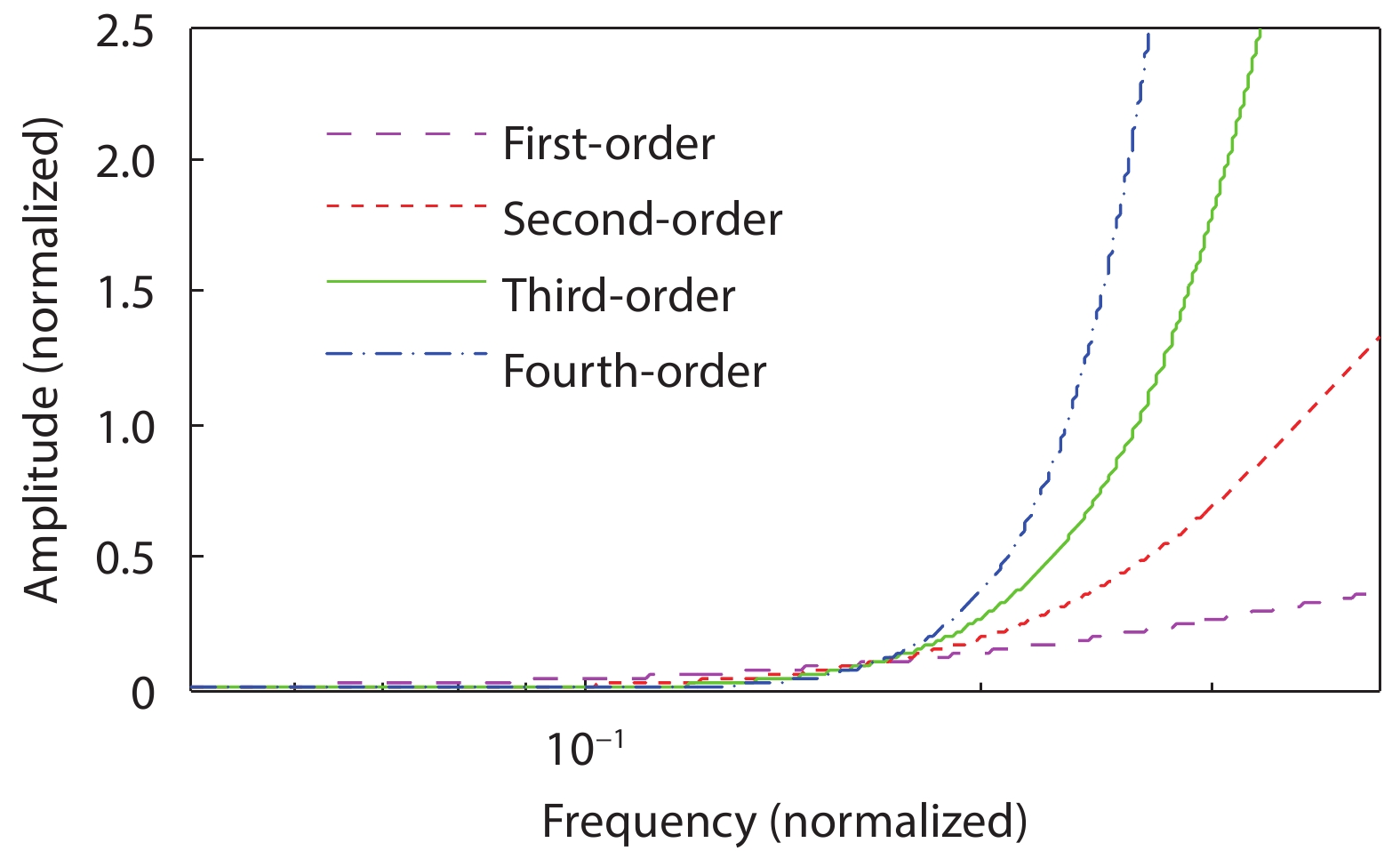
Fig. 1 shows the noise modulation results with different modulation orders. The results show that as the modulation order increases, more low-frequency noise is modulated into the high-frequency domain. The realization of a high precision ADC can be anticipated after back-end low-pass digital filter filtering of the high-frequency noise.
![]()
Figure 1.(Color online) Noise modulation under different modulation orders.
According to Ref. [17], the signal quantization noise rate (SQNR) can be expressed as follows:
where N is the modulation stages.
To realize a high-precision Σ–Δ ADC, a higher N and OSR leads to improved performance; however, as mentioned earlier, the stability and input range of the structure decreases with increasing modulation stages. In this work, N was designed as 4 and the OSR was selected as 128. By employing the Look-up table method to obtain zeros and the Butterworth filter method to get the poles[
The simulated relationship between the SQNR and the input signal amplitude is displayed in Fig. 2.
![]()
Figure 2.(Color online) Relationship of the SQNR with input signal amplitude.
The CIFB modulator is a cascade of several integrators with feedbacks. Fig. 3 displays the 4-order single-loop CIFB modulator structure designed in this work. The signal transfer function (STF) is a low-pass filter under the CIFB structure, which can suppress out of band signals.
![]()
Figure 3.4-order single-loop CIFB structure.
The NTF corresponding to the CIFB structure in Fig. 3 is as follows:
According to the NTF formula (2), the mapped CIFB parameters could be obtained, as shown in Table 1[
Fig. 4 depicts the designed NTF/STF transfer function, and Fig. 5 gives the simulated SQNR result under –6 dB input signal.
![]()
Figure 4.NTF/SFT transfer functions after mapping to CIFB structure.
![]()
Figure 5.(Color online) Simulated SQNR under –6 dB input after mapping to CIFB structure.
3. Circuit implementation
As Fig. 3 shows, the Σ–Δ modulator is essentially an IIR filter, which is cascaded with 4-stage integrators. Based on the work mode of the integrators, the Σ–Δ modulator can be divided into two classes: (1) continuous-time (CT) modulator and (2) switched-capacitor (SC) modulator. A CT modulator exhibits a higher bandwidth, low power dissipation, and contains an anti-aliasing circuit internally, so it is popular in wireless communication; however, CT modulation is more sensitive to clock jitter, feedback network delay, and resistor/capacitor mismatches arising from the manufacturing process, so achieving high precision is difficult. In contrast, the SC modulator is bandwidth limited (generally less than 1 MHz) but less sensitive to parameter fluctuation; hence, it is adopted widely for high precision Σ–Δ modulator designs. In this work, the SC modulator was employed to implement the CIFB structure, which is shown in Fig. 6.
![]()
Figure 6.SC implementation of the CIFB structure modulator.
According to Fig. 6, the following critical circuits need to be implemented: the bandgap reference circuit, the operation amplifier (OTA), the clock generator, the comparator (1-bit quantizer), and latch.
3.1. Bandgap reference
Essentially, the bandgap reference is a voltage reference generator circuit that employs two opposing temperature modulation mechanisms. The bandgap reference is ideally a zero-temperature drift voltage reference; however, because the positive or negative drift factors themselves depend on the temperature, it is hard to achieve absolute zero temperature drift voltage reference because of the presence of variances caused by the manufacturing process. Generally, over a wide temperature range, such as between –40 to 85 °C, 50-ppm/°C can be achieved. Fig. 7 shows the bandgap reference circuit designed in this work and Fig. 8 gives the simulated results.
![]()
Figure 7.Bandgap reference circuit.
![]()
Figure 8.Simulated results (bandgap voltage fluctuation with power supply and temperature).
3.2. OTA
In this work, a two-stage structure was adopted for the OTA, with the first stage providing high gain and the second stage providing a large swing. Wang et al.[
![]()
Figure 9.OTA circuit.
![]()
Figure 10.(Color online) Frequency Response of the designed OTA.
4. Clock generator
The SC modulator was a clock driven structure. As shown in Fig. 6, four clocks were needed S1, S1d, S2, and S2d, and the relationship of these clocks is displayed in Fig. 11.
![]()
Figure 11.Clocks used in the modulator.
The clock generator circuit was implemented as shown in Fig. 12. With the delay designated in the figure, the following relationship is obtained:
![]()
Figure 12.Clock generator circuit.
According to the simulation results in Fig. 13, switches with the same phase (S1/S1d or S2/S2d) turn on at the same time, while they turn off with a delay. An SC modulator requires that charge injection is avoided when the switches turn off.
![]()
Figure 13.Simulation results of clock generator.
5. Comparator and latch
The comparator is used as a 1-bit quantizer in the SC modulator. The comparator and latch are both digital circuits that have standard implementations. In this work, hysteresis was incorporated to avoid multiple-trigger issues because of close thresholds. The hysteresis essentially acts as a positive feedback system, and the comparator adopting this system is called a Schmitt comparator. The comparator and latch circuit implemented in this work are shown in Fig. 14.
![]()
Figure 14.Comparator and Latch incorporating a hysteresis.
6. Results
Based on the 4-order single-loop CIFB SC modulator structure with the circuits introduced in the previous section, a Σ–Δ modulator was implemented with a Chartered 0.35 μm CMOS process and a chip area of 1.72 × 0.75 mm2. The chip was operated with a 3.3-V power supply with a power dissipation of 22 mW. Fig. 15 shows the chip layout and Fig. 16 shows the layout architecture and the manufactured chip.
![]()
Figure 15.(Color online) Σ–Δ modulator layout.
![]()
Figure 16.Σ–Δ modulator (SDM) layout architecture and chip after manufacturing.
To thoroughly evaluate the chip performance, a test bench was designed for the chip and a mature industrial chip was used for comparison. The test bench architecture and the test board are displayed in Fig. 17.
![]()
Figure 17.(Color online) Test bench for the designed Σ–Δ modulator.
The test bench included the following components: signal source: CS4373, output high-precision sinusoidal wave with SNR > 114 dB; digital filter: CS5376 with comb filter, FIR filter, IIR filter internally; modulator for comparison: CS5372, high-precision Σ–Δ modulator used widely in the seismic exploration field.
Fig. 18 shows the modulated bit stream (time domain waveform) output of the designed Σ–Δ modulator. The bit stream outputs at the falling edge of the output clock. The bit rate was 512 kbps, which is the same as CS5372.
![]()
Figure 18.(Color online) Modulated bit stream output of the designed Σ–Δ modulator.
Fig. 19 shows a comparison of the raw modulated bit stream performance and Fig. 20 shows a performance comparison after digital filtering for both the designed and industrial (CS5372) chips. The designed chip shows improved performance compared with the mature industrial chip for some parameters. Table 3 summarizes the comparison results.
![]()
Figure 19.(Color online) Raw bit stream performance comparison of the designed chip with the industrial chip (CS5372).
![]()
Figure 20.(Color online) Performance comparison after digital filtering of the designed chip with the industrial chip (CS5372).
FOM-w (figure of merit-w) is a general evaluation index[
In addition to FOM-w, the FOM-v evaluation index[
According to the analysis in Section 2, the higher OSR and orders, the higher SNR, thus the higher ENOB would be achieved. The internal driver frequency is generally decided by the DOR: the higher the DOR, the higher the driver frequency, thus the higher the power dissipation. Another critical point is the power supply: the higher the power supply, the higher the power dissipation. Quantizer and process manufacture process play relatively less important roles than the previous factors. Special attention should be paid to the work of Brigati et al.[
7. Conclusion
In this paper, a 4-order single-loop SC modulator with a CIFB structure was proposed. Based on the proposed structure, the implementation of the critical circuits was illustrated and verified via simulations. The modulator chip was successfully manufactured using the Chartered 0.35 μm CMOS process, with a chip area of 1.72 × 0.75 mm2. The chip operated under a 3.3-V power supply with a power dissipation of 22 mW. The test results showed the designed modulator chip had improved performance compared with a mature industrial chip, and its ENOB was almost 18-bit. Therefore, it could be used in audio, digital TV, wireless communication and oil exploration, where demand high requirements for low frequency noise or high precision.
Acknowledgment
This paper has been funded by the Major Emerging Industrial Projects of Anhui, and the Postdoctoral Project from Hefei. The authors gratefully acknowledge the financial support and wish to express their thanks to the referees for critically reviewing the manuscript and making important suggestions.
References
[1] H Inose, H Inose, Y Yasuda et al. A telemetering system by code modulation — Δ–Σ modulation. IRE Trans Space Electron Telemetry, 8, 204(1962).
[2] G R Ritchie, J Candy, W Ninke. Interpolative digital to analog converters. IEEE Trans Commun, 22, 1797(1974).
[3] J C Candy. A use of limit cycle oscillations to obtain robust analog-to-digital converters. IEEE Trans Commun, 22, 298(1974).
[4] J C Candy, B Wooley, O Benjamin. A voiceband codec with digital filtering. IEEE Trans Commun, 29, 815(1981).
[5] J C Candy, O J Benjamin. The structure of quantization noise from sigma-delta modulation. IEEE Trans Commun, 29, 1316(1981).
[6] J C Candy. A use of double integration in sigma-delta modulations. IEEE Trans Commun, 33, 249(1985).
[7] J C Candy, A Huynh. Double Interpolation for digital-to-analog conversion. IEEE Trans Commun, 34, 77(1986).
[8] T Hayashi, e Y Inabe, K Uchimura et al. A multistage delta-sigma modulator without double integration loop. ISSCC Digest of Technical Papers, 182(1986).
[9] J Q Chen, J Y Ren, J Xun et al. An 80 dB dynamic range modulator for a GSM system. Chin J Semicond, 28, 294(2007).
[10] Y Cao, T L Ren, Z L Hong et al. A 16 bit 96 kHz chopper-stabilized sigma-delta ADC. Chin J Semicond, 28, 1204(2007).
[11] J Yuan, Z F Zhang, J Wu et al. Continuous time sigma delta ADC design and non-idealities analysis. J Semicond, 32, 125007(2011).
[12] R Li, J Li, T Yi et al. A 18-mW, 20-MHz bandwidth, 12-bit continuous-time modulator using a power-efficient multi-stage amplifier. J Semicond, 33, 015007(2012).
[13] T C Caldwell, D A Johns. An 8-th order MASH delta-sigma with an OSR of 3. ESSCIRC, 476(2009).
[14] J S Chiang, H L Chen, P C Chou. A 2.5-V 14-bit MASH sigma-delta modulator for ADSL. IEEE Asia-Pacific Conference on Advanced System Integrated Circuits, 24(2004).
[15]
[16] K C Chao, S Nadeem, W L Lee et al. A higher order topology for interpolative modulators for oversampling A/D converters. IEEE Trans Circuits Syst, 37, 309(1990).
[17]
[18] F Wang, R Harjani. Power analysis and optimal design of opamps for oversampled converters. IEEE Trans Circuits Syst II, 46, 359(1999).
[19] F Medeiro, B Pérez-Verdú, la Rosa J M de et al. Fourth-order cascade SC sigma delta modulator: a comparative study. IEEE Trans Circuits Syst I, 45, 1041(1998).
[20]
[21]
[22] P Balmelli, Q Huang. A 25 MS/s 14 b 200 mW Σ∆ modulator in 0.18
[23] S Brigati, i F Francesconi, P Malcovati et al. A Fourth-order singla-bit switched capacitor sigma delta modulator for distributed sensor applications. IEEE Trans Instrum Meas, 53, 266(2004).
[24] A Gerosa, A Neviani. A 1.8
[25] L Yao, M Steyaert, W Sansen. A 1-V, 1 MS/s, 88-dB sigma delta modulator in 0.13-
[26]

Set citation alerts for the article
Please enter your email address
© Copyright 2018-2021 | Chinese Laser Press. All Rights Reserved 沪ICP备15018463号-20