• Journal of Semiconductors
  • Vol. 40, Issue 12, 121802 (2019)
Linlin Su, Dong Zhou, Hai Lu, Rong Zhang, and Youdou Zheng
Author Affiliations
  • School of Electronic Science and Engineering, Nanjing University, Nanjing 210093 China
  • show less
    DOI: 10.1088/1674-4926/40/12/121802 Cite this Article
    Linlin Su, Dong Zhou, Hai Lu, Rong Zhang, Youdou Zheng. Recent progress of SiC UV single photon counting avalanche photodiodes[J]. Journal of Semiconductors, 2019, 40(12): 121802 Copy Citation Text show less
    (Color online) A schematic of various applications for UV detectors.
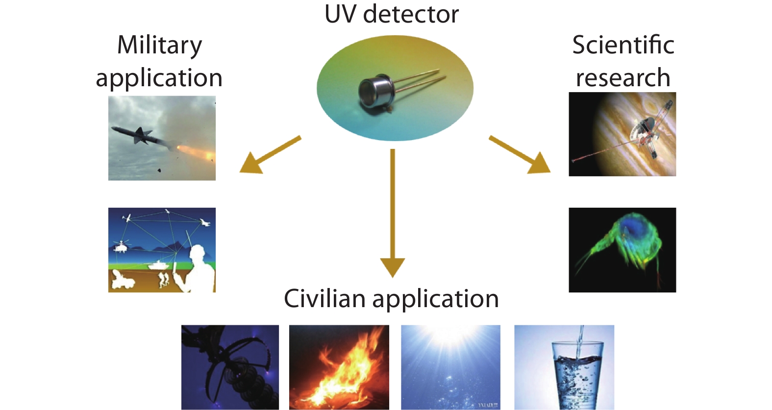
    Fig. 1. (Color online) A schematic of various applications for UV detectors.
    (Color online) Schematic of the (a) basic device structure and (b) avalanche multiplication mechanism of a working APD.
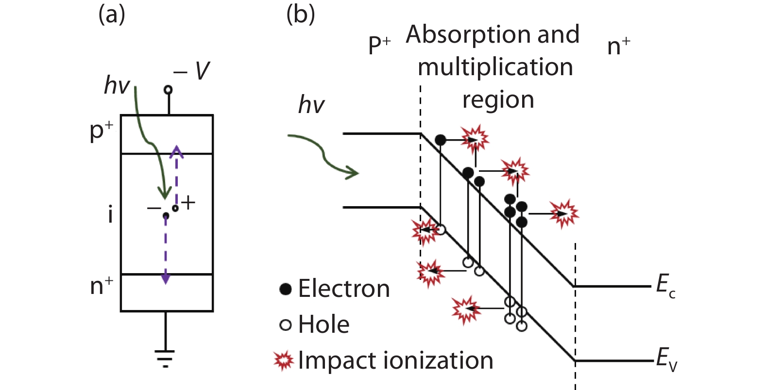
    Fig. 2. (Color online) Schematic of the (a) basic device structure and (b) avalanche multiplication mechanism of a working APD.
    (Color online) A schematic of gain–voltage curve of an APD working in either linear mode or Geiger mode.
    Fig. 3. (Color online) A schematic of gain–voltage curve of an APD working in either linear mode or Geiger mode.
    The process of impact ionization in (a) linear mode and (b) Geiger mode.
    Fig. 4. The process of impact ionization in (a) linear mode and (b) Geiger mode.
    (Color online) Area normalized DCR or DCP versus SPDE for SiC[20, 25–29], GaN[12, 24] and Si APDs[23].
    Fig. 5. (Color online) Area normalized DCR or DCP versus SPDE for SiC[20, 2529], GaN[12, 24] and Si APDs[23].
    (Color online) Typical scanning electron microscopy image from SiC epitaxial layer after molten KOH etching.
    Fig. 6. (Color online) Typical scanning electron microscopy image from SiC epitaxial layer after molten KOH etching.
    (Color online) (a) I–V and (b) DCR versus SPDE curves of four 4H-SiC APDs. From device A to D, EPDs in device active layers increase.
    Fig. 7. (Color online) (a) IV and (b) DCR versus SPDE curves of four 4H-SiC APDs. From device A to D, EPDs in device active layers increase.
    (Color online) The cross-sectional view of a SiC APD with bevel edge termination.
    Fig. 8. (Color online) The cross-sectional view of a SiC APD with bevel edge termination.
    (Color online) The simulated 2D electric field distribution of (a) a vertical mesa SiC APD, and (b) a beveled mesa SiC APD under avalanche breakdown voltage. The inset shows the 1-D electrical field profile along the black line marked in the 2-D electrical field profile.
    Fig. 9. (Color online) The simulated 2D electric field distribution of (a) a vertical mesa SiC APD, and (b) a beveled mesa SiC APD under avalanche breakdown voltage. The inset shows the 1-D electrical field profile along the black line marked in the 2-D electrical field profile.
    (Color online) Cross-sectional view of SiC APDs with a combined partial trench termination and deep trench isolation.
    Fig. 10. (Color online) Cross-sectional view of SiC APDs with a combined partial trench termination and deep trench isolation.
    (Color online) The simulated 2-D electric field distribution of a partial trench termination APD under avalanche breakdown voltage. The inset shows the 1-D electrical field profile along the black line marked in the 2-D electrical field profile.
    Fig. 11. (Color online) The simulated 2-D electric field distribution of a partial trench termination APD under avalanche breakdown voltage. The inset shows the 1-D electrical field profile along the black line marked in the 2-D electrical field profile.
    (Color online) The room temperature I–V and gain–voltage characteristics of a 4H-SiC APD.
    Fig. 12. (Color online) The room temperature IV and gain–voltage characteristics of a 4H-SiC APD.
    (Color online) Spectral response characteristics of a 4H-SiC APD at different bias.
    Fig. 13. (Color online) Spectral response characteristics of a 4H-SiC APD at different bias.
    Typical DCR versus SPDE curve of a 4H-SiC APD at room temperature.
    Fig. 14. Typical DCR versus SPDE curve of a 4H-SiC APD at room temperature.
    (Color online) Variation of DCR and SPDE as a function of temperatures for a SiC APD.
    Fig. 15. (Color online) Variation of DCR and SPDE as a function of temperatures for a SiC APD.
    (Color online) (a) Photocurrent of the three SiC APDs under same illumination condition at avalanche regime. (Inset) Top-view images of the three SiC APDs, which are denoted as APD 1, 2 and 3 respectively. (b) DCR-voltage and PCR-voltage characteristics of the three SiC APDs.
    Fig. 16. (Color online) (a) Photocurrent of the three SiC APDs under same illumination condition at avalanche regime. (Inset) Top-view images of the three SiC APDs, which are denoted as APD 1, 2 and 3 respectively. (b) DCR-voltage and PCR-voltage characteristics of the three SiC APDs.
    (Color online) Cross-sectional view of the recessed-window SiC APD.
    Fig. 17. (Color online) Cross-sectional view of the recessed-window SiC APD.
    (Color online) (a) Cross-sectional view of the SACM SiC APD. (b) Electric field profiles of SiC SACM APDs with reach-through structure and non-reach-through structure.
    Fig. 18. (Color online) (a) Cross-sectional view of the SACM SiC APD. (b) Electric field profiles of SiC SACM APDs with reach-through structure and non-reach-through structure.
    (Color online) The room temperature spectral response characteristics of the 4H-SiC SACM APD measured at different bias. Inset: spectral response characteristics plotted in linear scale.
    Fig. 19. (Color online) The room temperature spectral response characteristics of the 4H-SiC SACM APD measured at different bias. Inset: spectral response characteristics plotted in linear scale.
    (Color online) I–V characteristics of 4H-SiC APDs formed by Al implantation.
    Fig. 20. (Color online) IV characteristics of 4H-SiC APDs formed by Al implantation.
    (Color online) Capacitance-frequency characteristics of the SiC APDs formed by Al implantation as well as the SiC APDs fully formed by epitaxial growth.
    Fig. 21. (Color online) Capacitance-frequency characteristics of the SiC APDs formed by Al implantation as well as the SiC APDs fully formed by epitaxial growth.
    Real time DCR and PCR spectra of a SiC APD at the same over-bias.
    Fig. 22. Real time DCR and PCR spectra of a SiC APD at the same over-bias.
    (Color online) The SPC mapping profiles of a SiC APD at different over-bias.
    Fig. 23. (Color online) The SPC mapping profiles of a SiC APD at different over-bias.
    Hot carrier luminescence images of a SiC APD at different avalanche currents.
    Fig. 24. Hot carrier luminescence images of a SiC APD at different avalanche currents.
    (Color online) (a) Schematic of a 4H-SiC wafer with 4° offcut angle and the electrical field direction of the fabricated SiC APD. (b) Schematic of carrier drift path within the 4H-SiC APD.
    Fig. 25. (Color online) (a) Schematic of a 4H-SiC wafer with 4° offcut angle and the electrical field direction of the fabricated SiC APD. (b) Schematic of carrier drift path within the 4H-SiC APD.
    Parameter4H-SiC6H-SiC3C-SiCGaNSi
    Bandgap (eV)3.2632.43.391.12
    Saturation electron velocity (107 cm/s) 2222.51
    Electron mobility (cm2/(V·s)) 95060090010001400
    Hole mobility (cm2/(V·s)) 120755030600
    Dielectric constant (Å)9.7109.78.911.4
    Thermal conductivity (W/(cm·K))4.94.93.21.51.5
    Table 1. Comparison of physical properties for various semiconductors[1316].
    Linlin Su, Dong Zhou, Hai Lu, Rong Zhang, Youdou Zheng. Recent progress of SiC UV single photon counting avalanche photodiodes[J]. Journal of Semiconductors, 2019, 40(12): 121802
    Download Citation