
Linlin Su, Dong Zhou, Hai Lu, Rong Zhang, Youdou Zheng. Recent progress of SiC UV single photon counting avalanche photodiodes[J]. Journal of Semiconductors, 2019, 40(12): 121802
- Journal of Semiconductors
- Vol. 40, Issue 12, 121802 (2019)
Abstract
1. Introduction
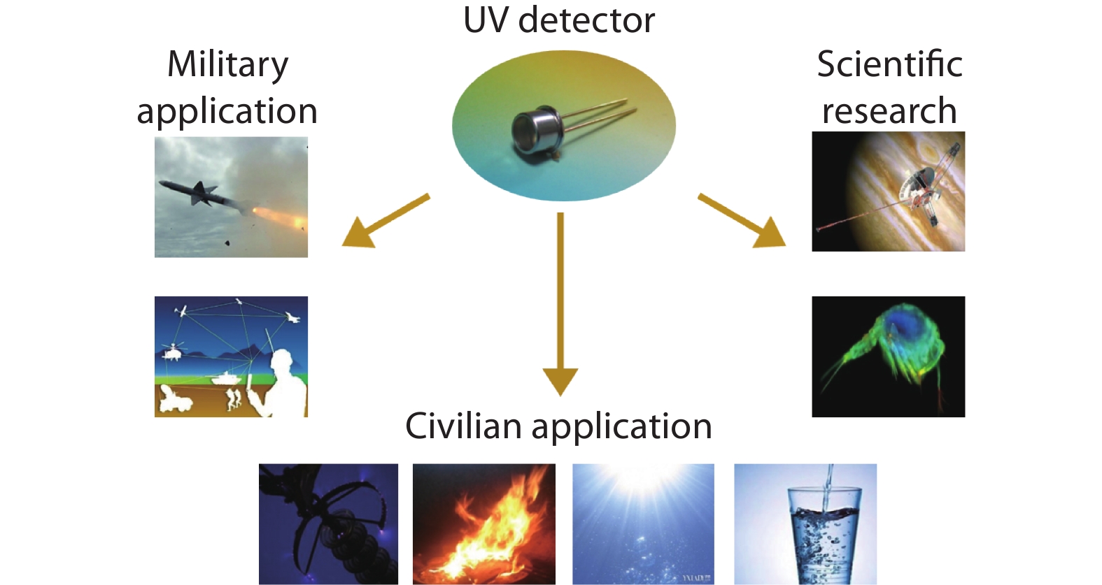
High sensitivity ultraviolet (UV) detectors[
![]()
Figure 1.(Color online) A schematic of various applications for UV detectors.
Until recently, photomultiplier tubes (PMTs) were the primary devices used for weak UV detection. Traditional PMTs and related imaging devices exhibit low dark counts and high gain, but suffer from many intrinsic drawbacks of the vacuum device, including high cost, bulky size, short lifetime and high operation voltage. Moreover, an additional filter is often required for PMTs used for UV detection. Therefore, for a long time, there has been a great need to replace PMTs with high performance solid-state UV detectors. Avalanche photodiodes (APDs) working in Geiger mode are attractive candidates for weak UV detection due to their small size, high multiplication gain and high quantum efficiency. Si based APDs benefit from advanced material and processing technologies. Although Si APDs do have sensitivity in the UV wavelength region, the cutoff wavelength of Si APDs is located in the near-infrared band[
Over these years, many studies have focused on improving the performance of 4H-SiC APDs, and great progress has been made. Various termination and device structures were investigated to realize high efficiency SiC APDs. New characterization techniques were applied to study their noise and degradation mechanisms. In this paper, the operation principles, key characteristics and design methods of SiC APDs will be reviewed and discussed.
2. Basic characteristics of SiC APDs
2.1. Principle of avalanche multiplication
Fig. 2 shows the structure and energy band diagram of a working APD. When light enters the active layer of SiC APDs, electron–hole pairs are generated if the photon energy is larger than the bandgap energy of SiC and the UV photon is absorbed. Under the influence of junction electrical field, electrons would drift towards n+ contact layer while holes would drift towards p+ contact layer. The drift velocity of photo-carriers relies on electric field strength, degree of scattering as well as acceleration distance. If the reverse voltage is high enough, photo-carriers would gain sufficient kinetic energy which, through collisions with the crystal lattice, would generate new electron–hole pairs. These electron–hole pairs would be accelerated again and then create additional electron–hole pairs in a process like a chain reaction. This process is known as avalanche multiplication of photo-carriers.
![]()
Figure 2.(Color online) Schematic of the (a) basic device structure and (b) avalanche multiplication mechanism of a working APD.
Fig. 3 shows a typical gain–voltage curve of an APD. APDs can work in either linear mode or Geiger mode depending on the magnitude of the reverse bias applied on the APD. The processes of impact ionization for the two operation modes are shown in Fig. 4. Linear mode is defined as the applied voltage slightly lower than the breakdown voltage of the APD, in which the avalanche multiplication gain of photo-carriers is relatively low. The linear mode gain is moderate and affected by excess noise, making detection of single photons difficult. Comparatively, Geiger mode is defined when the applied bias is higher than the breakdown voltage, in which the avalanche multiplication gain is very high, typically in the range of 105 to 106. In this operation mode, the junction electric field is so high that both holes and electrons would participate in the process of impact ionization, resulting in a self-sustaining avalanche process. Then even a single charge carrier injected into the multiplication layer could trigger a high avalanche current, which makes ultra-weak light detection and even single photon counting possible. As a result, Geiger mode APDs are also called SPADs.
![]()
Figure 3.(Color online) A schematic of gain–voltage curve of an APD working in either linear mode or Geiger mode.
![]()
Figure 4.The process of impact ionization in (a) linear mode and (b) Geiger mode.
Since in Geiger operation mode the avalanche multiplication process is a self-sustaining process, to realize single photon counting, the avalanche current has to be quenched by an external circuit, so that the APD could recover to its original state and is ready to detect the next incoming photon. The function of quenching circuits is to quickly quench the rising avalanche current by temporally reducing the applied bias on the APD. Commonly used quenching schemes include a passive quenching circuit, active quenching circuit and gated quenching circuit.
2.2. Key performance parameters of APDs
2.2.1. Dark count rate (DCR)
Even in the absence of light illumination, the output of a photodiode is not zero but is disturbed by noise signals. In the case of SPADs, the noise signals are called dark counts, which are pulse signals in the quenching circuit induced by leakage current or the thermal current of the APD. In addition, an after pulsing effect is another mechanism for DCR. After pulsing is caused by a carrier trapping and detrapping effect. During avalanche multiplication, multiplied carriers can be captured by defects in the depletion layer and released subsequently. These carriers can re-trigger avalanche multiplication under high electrical field, generating new counts in the circuit. Normally, DCR could be lowered by reducing the operation temperature or improving the crystalline quality of the APD epi-structure.
2.2.2. Single photon detection efficiency (SPDE)
SPDE is the probability of each incident photon to be individually detected. SPDE can be presented by the following equation:
where PCR is photon count rate of the APD under UV illumination, Fil is the density of incident photons, Ff is fill factor of the APD, QE is quantum efficiency of the APD without avalanche multiplication, and PAP is photon avalanche probability, which is the probability of an excited photon-carrier to generate an avalanche event. In Fig. 5, DCR or dark count probability (DCP) versus SPDE (normalized to an active area of 100 μm in diameter) for 4H-SiC APDs are shown together with those published results of GaN APDs and Si APDs. Nowadays the highest SPDE approaching 50% has been obtained in silicon APDs with the lowest DCR of low—103 Hz at 530 nm[
![]()
Figure 5.(Color online) Area normalized DCR or DCP versus SPDE for SiC[
3. Key factors affecting the performance of SiC APDs
3.1. Material defects
Since APD works under a very high electrical field, structural defects in the device active layer could easily cause catastrophic breakdown of the APD. Meanwhile, structural defects are also the cause of high DCR and low SPDE. Thus, very high crystalline quality is required for APD fabrication. Over the past ten years, material quality of SiC substrate and epi-structure has seen steady improvement benefiting from the large investment on the development of SiC power devices.
Although 6-inch conductive n-type 4H-SiC substrates have become the mainstream of power device fabrication, SiC epitaxial wafers still contain a variety of defects, such as threading dislocations, basal plane dislocations, stacking faults and point defects. Micro-pipes used to be major killer defects for SiC devices, but its density has dropped to less than 1 cm–2. Therefore, currently structural defects other than micro-pipes are the major cause of defect-related premature breakdown. It is important to map the defect distribution of the epi-layer and establish a correlation between the defect profile and device performance. Structural defects in SiC have been observed by several methods, such as molten KOH etching[
![]()
Figure 6.(Color online) Typical scanning electron microscopy image from SiC epitaxial layer after molten KOH etching.
Besides leading to premature breakdown and reliability problems, structural defects normally degrade APD performance by increasing dark current and dark counts. Fig. 7 shows the dark current–voltage (I–V) characteristics and DCR versus SPDE curves of four SiC APDs with increased EPD in device active layer from device A to device D. It is clear that device A exhibits the lowest dark current, the sharpest avalanche breakdown curve and the smallest DCR at the same SPDE. In addition, the DCRs of all four devices increase at higher SPDE as shown in Fig. 7(b). For an APD device, both DCR and SPDE are closely related to the avalanche multiplication probability, which increases with the rise of the junction electric field. Thus, a higher SPDE could be obtained at higher overbias, nevertheless the DCR would increase too. In order to investigate the physical mechanisms of dark current in SiC APD, temperature dependent reverse I–V characteristics can be used to derive the activation energy of the dark current based on an Arrhenius plot. If the activation energy is close to the bandgap energy of SiC, the origin of the dark current is a diffusion current from quasi-neutral region[
![]()
Figure 7.(Color online) (a)
Similar to dark current, there are four main sources of DCR: (a) carriers diffused from the quasi-neutral region into the depletion region, (b) thermal carriers generated in the depletion region, (c) band-to-band tunneling, (d) trap-assisted tunneling. If DCR shows a trend of exponential increase as a function of excess bias, the carrier tunneling mechanism is likely the main cause of DCR[
3.2. Edge termination
Since APD works under very high electrical field, effective edge termination is critical for reliable operation. Meanwhile, if a strong peak electrical field exists around the device edge, large gain non-uniformity across the device active layer would degrade the APD overall performance. In past studies, a two-dimensional raster scan of the photocurrent indeed shows a sharp photocurrent peak around the device mesa edge, indicating the presence of enhanced edge breakdown[
Since the critical electrical field of 4H-SiC is as high as 3.3 MV/cm, to fabricate a SiC APD with operation voltage less than 300 V, the multiplication layer thickness of the APD could not exceed 1 μm. This situation means that many mature termination structures used in SiC power devices cannot be used for SiC APDs. Currently, beveled mesa edge termination is mostly used for SiC APDs, which has been verified to effectively suppress electrical field crowding effect around the mesa edge. As shown in Fig. 8, the beveled mesa with a positive bevel angle less than 10˚ can be formed by dry etching following a photoresist reflow technique. Through increasing depletion width around mesa edge, the edge electrical field is lowered, which allows bulk breakdown to precede edge breakdown[
![]()
Figure 8.(Color online) The cross-sectional view of a SiC APD with bevel edge termination.
![]()
Figure 9.(Color online) The simulated 2D electric field distribution of (a) a vertical mesa SiC APD, and (b) a beveled mesa SiC APD under avalanche breakdown voltage. The inset shows the 1-D electrical field profile along the black line marked in the 2-D electrical field profile.
Besides beveled mesa termination, a double mesa termination is also developed for SiC APDs[
3.3. Surface passivation
Surface leakage could be a large dark current component in SiC APDs, which gradually increases at higher bias even at low voltage range. Surface leakage is not as harmful as bulk leakage, which does not necessarily cause dark counts. Nevertheless, surface leakage normally links with surface/interface defects, which would cause other reliability problems. Surface defects in SiC wafers have been widely observed, and the activation energy is determined to be ~0.4–0.54 eV by deep level transient spectroscopy[
4. High performance SiC APDs development
4.1. 4H-SiC APDs with high fill factor
Until recently, to prevent edge breakdown a small-angle beveled mesa termination structure has been widely adopted in SiC APDs. In order to effectively suppress an edge peak electrical field, a small bevel angle of less than 10˚ is normally required. Nevertheless, in those reported structures, the devices are fully trench isolated with its mesa being etched all the way down to the bottom contact layer. In this case, the mesa sidewall would occupy a fairly large device area, resulting in significantly reduced fill factor. This disadvantage would become more serious for small diameter devices, which are often used for imaging arrays. To overcome this problem, SiC APDs could adopt a partial trench termination scheme[
![]()
Figure 10.(Color online) Cross-sectional view of SiC APDs with a combined partial trench termination and deep trench isolation.
![]()
Figure 11.(Color online) The simulated 2-D electric field distribution of a partial trench termination APD under avalanche breakdown voltage. The inset shows the 1-D electrical field profile along the black line marked in the 2-D electrical field profile.
Fig. 12 shows the room-temperature I–V and gain-voltage characteristics of a partial trench termination SiC APD (~ 150 μm). Its dark current remains at ~ 0.1 pA level at 95% breakdown voltage, and a high avalanche gain of over 5 × 10⁵ can be obtained at an overbias of 2 V. As shown in Fig. 13, its spectral response curves peaks at ~ 285 nm with a responsivity of 0.1517 A/W under 0 V bias, corresponding to a maximum quantum efficiency of ~ 66%. The low-bias UV/visible (285 nm/400 nm) rejection ratio is ~ 8 × 10³. As the bias increases to 200 V, the peak responsivity wavelength remains at ~ 285 nm with almost unchanged rejection ratio. Comparatively, the absorption edge of GaN APDs is strongly affected by the Frantz-Keldysh effect, which could extend to blue band under high electrical field[
![]()
Figure 12.(Color online) The room temperature
![]()
Figure 13.(Color online) Spectral response characteristics of a 4H-SiC APD at different bias.
![]()
Figure 14.Typical DCR versus SPDE curve of a 4H-SiC APD at room temperature.
![]()
Figure 15.(Color online) Variation of DCR and SPDE as a function of temperatures for a SiC APD.
Meanwhile, optimization of electrode shape is another approach to enhance SiC APD’s fill factor. It is because SiC APDs are grown on a conductive SiC substrate by homo-epitaxy. There is no “window layer” in SiC APD structure, so the device has to work in front-illumination mode. Thus, the top contact layer of the APD would itself strongly absorb a usable UV signal but contribute little photocurrent. Thus, normally the top contact layer of SiC APDs is designed to be quite thin. Due to the presence of lateral resistance of the top contact layer, the junction electric field strength in the region away from the contact electrode would decrease as the distance from the electrode increases. As a result, the impact ionization effect in those regions is weakened, leading to non-uniform avalanche multiplication gain across the device mesa. Adopting a branch-shaped top-electrode is a method to reduce the size of electrode non-covered region, which could realize a relatively uniform junction electric field distribution and then enhance fill factor. To confirm this idea, three different top-electrode patterns with a traditional dot electrode and four or six branch electrode (inset in Fig. 16(a)) are designed in SiC APDs by Yang et al.[
![]()
Figure 16.(Color online) (a) Photocurrent of the three SiC APDs under same illumination condition at avalanche regime. (Inset) Top-view images of the three SiC APDs, which are denoted as APD 1, 2 and 3 respectively. (b) DCR-voltage and PCR-voltage characteristics of the three SiC APDs.
4.2. Recessed-window 4H-SiC APDs
Again, due to the limited conductivity of the top contact layer, there is a contradiction in SiC APD design. If the top contact layer is thick, significant portion of UV photons would be absorbed by the top contact layer. The situation is worse for deep UV light detection due to the reduced penetration depth at shorter wavelength. If the top contact layer is thin, limited conductivity of the layer would result in poor photo-carrier collection efficiency and avalanche non-uniformity. In addition, since ohmic metallization reaction would consume certain thickness of SiC material, if the top contact layer is too thin, alloy reaction related uneven interface could easily lead to punch through of the SiC APD at high electrical field. Therefore, the thickness of the top contact layer is an important design parameter in SiC APDs.
One way to lessen the above contradiction is to design a SiC APD with a recessed-window layer. Fig. 17 shows the structure of a recessed-window SiC APD, which could reduce the photon absorption and carrier recombination in the top contact layer while maintaining the integrity of the ohmic contact region. A 50% quantum efficiency increase has been reported for a recessed-window APD compared to its control non-recessed APD[
![]()
Figure 17.(Color online) Cross-sectional view of the recessed-window SiC APD.
4.3. Separated absorption charge multiplication (SACM) 4H-SiC APDs
A low operation voltage is always desired for APD applications, which is not only beneficial for reducing power consumption, but also helpful for improving the breakdown voltage consistency in APD-based imaging arrays. A straight-forward approach to decrease the operation voltage is to use a relatively thin multiplication layer. However, as an indirect bandgap semiconductor, SiC has a relatively low optical absorption coefficient. Reducing the multiplication layer thickness means insufficient absorption of UV light and a correspondingly low QE. To solve this problem, SiC APDs can be designed to have separated absorption and multiplication layers[
SACM APDs are traditionally designed to work in reach-through mode, in which a high electric field extends through the whole active layer. That is, multiplication, charge control, and absorption layers are all fully depleted. This design enhances the chance that photo-generated carriers in the absorption region are swept into the multiplication region and then contribute to the impact ionization process. However, the dark current would also increase due to the additional drift current induced by the strong electric field in the absorption region, which decreases the signal-to-noise ratio of the APD. Alternatively, a non-reach-through SACM design has been proposed to reduce the high-field-induced dark current, in which its absorption layer is not fully depleted. Fig. 18 shows the corresponding cross-sectional view and electric field profiles of a SiC SACM APD. A high low-bias peak quantum efficiency of ~ 80% at 280 nm has been achieved in SiC SACM APDs (Fig. 19). In addition, a SPDE of 9.4% and a DCP of 4 × 10⁻⁴ is demonstrated at wavelength of 266 nm[
![]()
Figure 18.(Color online) (a) Cross-sectional view of the SACM SiC APD. (b) Electric field profiles of SiC SACM APDs with reach-through structure and non-reach-through structure.
![]()
Figure 19.(Color online) The room temperature spectral response characteristics of the 4H-SiC SACM APD measured at different bias. Inset: spectral response characteristics plotted in linear scale.
4.4. 4H-SiC APDs with Al ion implantation
Nowadays, the growth of a p-type SiC layer is normally not desired in commercial production scale SiC epitaxial reactors, which is largely devoted to power device fabrication. The memory effect of p-type dopants in later growth runs is being concerned. In order to overcome this problem, p-type doping could be alternatively achieved by ion implantation, which is already a standard processing technique used in SiC power devices[
For SiC APDs formed by Al ion implantation[
![]()
Figure 20.(Color online)
![]()
Figure 21.(Color online) Capacitance-frequency characteristics of the SiC APDs formed by Al implantation as well as the SiC APDs fully formed by epitaxial growth.
In addition, the development of ion implantation-based doping in SiC APDs has another advantage. It could be used for realizing fully planer APD devices, which have many benefits compared with mesa type APDs in terms of reliability and electrical field confinement. A prototype fully planar SiC APD has been reported by Sciuto et al. with certain success[
5. Uniformity of avalanche multiplication in 4H-SiC APDs
As a key performance parameter of Geiger-mode APDs, SPDE is calculated by dividing the number of total single photon counts (SPCs) by the number of all incident photons. SPDE is proportional to avalanche probability (Pa) of photo-carriers, which is strongly related to the electric field strength within the APD multiplication layer. Whereas, if structural defects or non-ideal termination structures exist, Pa could vary considerably across the device active area, leading to device performance degradation and reliability problem. Fig. 22 shows the real-time DCR and PCR spectra of a SiC APD biased at the same voltage recorded by an oscilloscope. Each count is signaled by a voltage pulse. It is clear that these voltage pulses have a wide distribution of heights, ranging from several mV to tens of mV. This observation suggests that photo-carriers within the APD experience fairly different degrees of avalanche multiplication, which would certainly degrade SPDE. Thus, it is important to know the actual uniformity profile of avalanche multiplications across the active region of 4H-SiC APDs.
![]()
Figure 22.Real time DCR and PCR spectra of a SiC APD at the same over-bias.
Several studies on photocurrent spatial uniformity of APDs have been published. Guo et al. reported a non-uniform photoresponse at high gain by raster-scan of the photocurrent across the APD mesa, and they concluded that the non-uniform avalanche multiplication is associated with variation of doping density as suggested by C–V measurement[
![]()
Figure 23.(Color online) The SPC mapping profiles of a SiC APD at different over-bias.
In addition, imaging hot carrier luminescence from an APD at avalanche regime is an alternative optical method to characterize gain uniformity, which is potentially faster and relatively straightforward. Hot carrier luminescence in reverse-biased p–n junctions is a known concept in literature, even if the number of emitted photons is small (previous studies have shown that every ~105 to 106 avalanche carriers would emit one photon)[
![]()
Figure 24.Hot carrier luminescence images of a SiC APD at different avalanche currents.
In order to understand the above avalanche multiplication non-uniformity revealed by hot carrier luminescence imaging, a physical model is proposed according to the off-orientation growth of SiC[
![]()
Figure 25.(Color online) (a) Schematic of a 4H-SiC wafer with 4° offcut angle and the electrical field direction of the fabricated SiC APD. (b) Schematic of carrier drift path within the 4H-SiC APD.
The non-uniform avalanche multiplication related to substrate misorientation can be ameliorated by design optimization of the top metal contact, which is effective to enhance carrier collection efficiency. Another approach is to intentionally design an asymmetric termination structure, which at high applied bias would lead to asymmetric junction electrical field around the mesa edge. This effect could be used to offset the carrier screening induced junction field asymmetry.
6. Conclusions
In this review, recent progress on design and fabrication of 4H-SiC APDs has been presented, which have great potential to replace traditional PMTs used for ultra-weak UV signal detection. Solid state UV detectors have many advantages, such as high efficiency, small size, long lifetime, and ease of integration. Over the past 15 years, many studies have been devoted to improve the performance of Geiger-mode SiC UV APDs. Although impressive progress has been made for SiC APDs, several challenges and existing problems should be addressed for future development:
(1) The DCR of current SiC APDs is still relatively high, which is considerably larger than theoretical estimation for wide bandgap semiconductors. The high DCR is mostly caused by defect-assisted tunneling, which is presumably point defect related. Thus, improving material quality is still critical for further enhancing the performance of SiC APDs.
(2) Non-uniform avalanche multiplication across device mesa is also an important factor influencing device overall performance. The degree of avalanche multiplication non-uniformity can be revealed by SPC mapping or hot carrier luminescence. Design optimization is a major approach to improve lateral avalanche uniformity. Meanwhile, new epi-structure design based on the concept of “avalanche engineering” also has good potential to remarkably improve device performance.
(3) In order to realize high quality weak signal UV imaging, focal plane arrays (FPAs) based on SiC SPADs should be developed. Besides single pixel performance, performance consistency among different SPAD pixels is a new challenge. Since the degree of impact ionization strongly depends on electric field strength, a very small variation of breakdown voltage would cause considerably different gain if a same bias is applied on all pixels. Thus, highly uniform SiC epi-material and processing technologies are required for FPA fabrication. Meanwhile, novel design of readout circuits for SiC SPAD arrays could be implemented, which can individually regulate applied bias on each SPAD pixel to achieve consistent avalanche gain.
Acknowledgement
This work is supported in part by National Key R&D Program of China under Grant No. 2016YFB0400902; and in part by the Priority Academic Program Development of Jiangsu Higher Education Institutions.
References
[1] M Razeghi. Short-wavelength solar-blind detectors-Status, prospects, and markets. Proc IEEE, 90, 1006(2002).
[2] J C Campbell. Recent advances in avalanche photodiodes. J Lightwave Technol, 34, 278(2016).
[3] Y Wang, Y Qian, X Kong. Photon counting based on solar-blind ultraviolet intensified complementary metal–oxide–semiconductor (ICMOS) for corona detection. IEEE Photonics J, 10, 1(2018).
[4] B Li, g W Jiang, g Y Liang. Solar-blinded detector by UV radiation from missile plume. Aerosp Electron Warf, 22, 7(2006).
[5] H Chen, K Liu, L Hu et al. New concept ultraviolet photodetectors. Mater Today, 18, 493(2015).
[6] D Zamora, A Torres. Method for outlier detection: a tool to assess the consistency between laboratory data and ultraviolet-visible absorbance spectra in wastewater samples. Water Sci Technol, 69, 2305(2014).
[7] Y Kumamoto, K Fujita, N I Smith et al. Deep-UV biological imaging by lanthanide ion molecular protection. Biomed Opt Express, 7, 158(2016).
[8] M Razeghi. Deep ultraviolet light-emitting diodes and photodetectors for UV communications. Proc SPIE, 5729, 30(2005).
[9] J C Jackson, D Phelan, A P Morrison et al. Toward integrated single-photon-counting microarrays. Opt Eng, 42, 112(2002).
[10] T Isoshima, Y Isojima, K Hakomori et al. Ultrahigh sensitivity single-photon detector using a Si avalanche photodiode for the measurement of ultraweak biochemiluminescence. Rev Sci Instrum, 66, 2922(1995).
[11] E Munoz, E Monroy, J L Pau et al. III nitrides and UV detection. J Phys-Condens Mat, 13, 7115(2001).
[12] J L Pau, R Mcclintock, K Minder et al. Geiger-mode operation of back-illuminated GaN avalanche photodiodes. Appl Phys Lett, 91, 41104(2007).
[13] M Roschke, F Schwierz. Electron mobility models for 4H, 6H, and 3C SiC. IEEE Trans Electron Devices, 48, 1442(2001).
[14] S J Pearton, J C Zolper, R J Shul et al. GaN: Processing, defects, and devices. J Appl Phys, 86, 1(1999).
[15] E Monroy, S F Omn, F Calle. Wide-bandgap semiconductor ultraviolet photodetectors. Semicond Sci Tech, 18, R33(2003).
[16] A R Powell, L B Rowland. SiC materials-progress, status, and potential roadblocks. Proc IEEE, 90, 942(2002).
[17] F Yan, Y Luo, J H Zhao et al. 4H-SiC visible bling UV avalanche photodiode. Electron Lett, 35, 929(1999).
[18] X Xin, F Yan, F Yan et al. Demonstration of 4H-SiC UV single photon counting avalanche photodiode. Electron Lett, 41, 212(2005).
[19] A L Beck, G Karve, S Wang et al. Geiger mode operation of ultraviolet 4H-SiC avalanche photodiodes. IEEE Photon Technol Lett, 17, 1507(2005).
[20] G A Shaw, A M Siegel, J Model et al. Deep UV photon-counting detectors and applications. Proc SPIE, 7320, 1(2009).
[21] A L Beck, X Guo, H Liu et al. Low dark count rate 4H-SiC Geiger mode avalanche photodiodes operated under gated quenching at 325 nm. Proc SPIE, 6372, 63720O-1(2006).
[22] L Li, D Zhou, H Lu et al. 4H-SiC avalanche photodiode linear array operating in Geiger Mode. IEEE Photonics J, 9, 6804207(2017).
[23] A Restelli, I Rech, P Maccagnani et al. Monolithic silicon matrix detector with 50
[24] E Cicek, Z Vashaei, R Mcclintock et al. Geiger-mode operation of ultraviolet avalanche photodiodes grown on sapphire and free-standing GaN substrates. Appl Phys Lett, 96, 261107(2010).
[25] X Bai, H Liu, D C Mcintosh et al. High-detectivity and high-single-photon-detection-efficiency 4H-SiC avalanche photodiodes. IEEE J Quantum Elect, 45, 300(2009).
[26] A Vert, S Soloviev, P Sandvik. SiC avalanche photodiodes and photomultipliers for ultraviolet and solar-blind light detection. Phys Status Solidi A, 206, 2468(2009).
[27] X Bai, D Mcintosh, H Liu et al. Ultraviolet single photon detection with Geiger-mode 4H-SiC avalanche photodiodes. IEEE Photon Technol Lett, 19, 1822(2007).
[28] L Li, D Zhou, F Liu et al. High fill-factor 4H-SiC avalanche photodiodes with partial trench isolation. IEEE Photon Technol Lett, 28, 2526(2016).
[29] D Zhou, F Liu, H Lu et al. High-temperature single photon detection performance of 4H-SiC avalanche photodiodes. IEEE Photon Technol Lett, 26, 1136(2014).
[30] T Kimoto. Material science and device physics in SiC technology for high-voltage power devices. Jpn J Appl Phys, 54, 040103(2015).
[31] T Katsuno, Y Watanabe, H Fujiwara et al. Analysis of surface morphology at leakage current sources of 4H-SiC Schottky barrier diodes. Appl Phys Lett, 98, 222111(2011).
[32] S Usami, Y Ando, A Tanaka et al. Correlation between dislocations and leakage current of p-n diodes on a free-standing GaN substrate. Appl Phys Lett, 112, 182106(2018).
[33] Y Yang, Z Chen. Identification of SiC polytypes by etched Si-face morphology. Mater Sci Semicond Proc, 12, 113(2009).
[34] Q Wahab, A Ellison, A Henry et al. Influence of epitaxial growth and substrate-induced defects on the breakdown of 4H-SiC Schottky diodes. Appl Phys Lett, 76, 2725(2000).
[35] B Chen, H Matsuhata, T Sekiguchi et al. Surface defects and accompanying imperfections in 4H-SiC: Optical, structural and electrical characterization. Acta Mater, 60, 51(2012).
[36] S Maimon, G W Wicks. nBn detector, an infrared detector with reduced dark current and higher operating temperature. Appl Phys Lett, 89, 151109(2006).
[37] X Ji, B Liu, Y Xu et al. Deep-level traps induced dark currents in extended wavelength In
[38] G A M Hurkx, D B M Klaassen, M P G Knuvers. A new recombination model for device simulation including tunneling. IEEE Trans Electron Dev, 39, 331(1992).
[39] A Vilà, J Trenado, A Arbat et al. Characterization and simulation of avalanche photodiodes for next-generation colliders. Sens Actuators A, 172, 181(2011).
[40] R Stephen. Performance of In
[41] S Yang, D Zhou, X Cai et al. Analysis of dark count mechanisms of 4H-SiC ultraviolet avalanche photodiodes working in Geiger Mode. IEEE Trans Electron Devices, 64, 4532(2017).
[42] A L Beck, B Yang, X Guo et al. Edge breakdown in 4H-SiC avalanche photodiodes. IEEE J Quantum Electron, 40, 321(2004).
[43] R L Davies, F E Gentry. Control of electric field at surface of P–N junction. IEEE Trans Electron Devices, 11, 313(1964).
[44] H Liu, X Zheng, Q Zhou et al. Double mesa sidewall silicon carbide avalanche photodiode. IEEE J Quantum Elect, 45, 1524(2009).
[45] X Guo, A L Beck, X Li et al. Study of reverse dark current in 4H-SiC avalanche photodiodes. IEEE J Quantum Elect, 41, 562(2005).
[46] K Yamaguchi, T Teshima, H Mizuta. Numerical analysis of an anomalous current assisted by locally generated deep traps in pn junctions. IEEE Trans Electron Devices, 46, 1159(1999).
[47] S Shen, Y Zhang, D Yoo et al. Performance of deep ultraviolet GaN avalanche photodiodes grown by MOCVD. IEEE Photon Technol Lett, 19, 1744(2007).
[48] S Yang, D Zhou, W Xu et al. 4H-SiC ultraviolet avalanche photodiodes with small gain slope and enhanced fill factor. IEEE Photonics J, 9, 1(2017).
[49] H Liu, D Mcintosh, X Bai et al. 4H-SiC PIN recessed-window avalanche photodiode with high quantum efficiency. IEEE Photon Technol Lett, 20, 1551(2008).
[50] X Cai, D Zhou, S Yang et al. 4H-SiC SACM avalanche photodiode with low breakdown voltage and high UV detection efficiency. IEEE Photonics J, 8, 1(2016).
[51] H Cha, S Soloviev, S Zelakiewicz et al. Temperature dependent characteristics of nonreach-through 4H-SiC separate absorption and multiplication APDs for UV detection. IEEE Sens J, 8, 233(2008).
[52] H Cha, S Soloviev, G Dunne et al. Comparison of 4H-SiC separate absorption and multiplication region avalanche photodiodes structures for UV detection. Proc 5th IEEE Conf Sensors, 5, 14(2006).
[53] A Vert, S Soloviev, J Fronheiser et al. Solar-blind 4H-SiC single-photon avalanche diode operating in Geiger Mode. IEEE Photon Technol Lett, 20, 1587(2008).
[54] S I Soloviev, A V Vert, J Fronheiser et al. Solar-blind 4H-SiC avalanche photodiodes. Mater Sci Forum, 615–617, 873(2009).
[55] W Sung, A Q Huang, B J Baliga. Bevel junction termination extension-a new edge termination technique for 4H-SiC high-voltage devices. IEEE Electron Device Lett, 36, 594(2015).
[56] Q Zhang, R Callanan, M K Das et al. SiC power devices for microgrids. IEEE Trans Power Electron, 25, 2889(2010).
[57] S Yang, D Zhou, H Lu et al. 4H-SiC p–i–n ultraviolet avalanche photodiodes obtained by Al implantation. IEEE Photon Technol Lett, 28, 1185(2016).
[58] S Yang, D Zhou, H Lu et al. High-performance 4H-SiC p–i–n ultraviolet photodiode with p layer formed by Al implantation. IEEE Photon Technol Lett, 28, 1189(2016).
[59] A Sciuto, M Mazzillo, P Lenzi et al. Fully planar 4H-SiC avalanche photodiode with low breakdown voltage. IEEE Sens J, 17, 4460(2017).
[60] X Y Guo, A L Beck, J C Campbell et al. Spatial nonuniformity of 4H-SiC avalanche photodiodes at high gain. IEEE J Quantum Elect, 41, 1213(2005).
[61] X Cai, C Wu, H Lu et al. Single photon counting spatial uniformity of 4H-SiC APD characterized by SNOM-based mapping system. IEEE Photon Technol Lett, 29, 1603(2017).
[62] C Banc, E Bano, T Ouisse et al. Photon emission analysis of defect-free 4H-SiC pn diodes in avalanche regime. Mater Sci Forum, 389–393, 1293(2002).
[63] S I Soloviev, P M Sandvik, A Vertiatchikh et al. Observation of luminescence from defects in 4H-SiC APDs operating in avalanche breakdown. Mater Sci Forum, 600–603, 1211(2008).
[64] L Su, X Cai, H Lu et al. Spatial non-uniform hot carrier luminescence from 4H-SiC p–i–n avalanche photodiodes. IEEE Photon Technol Lett, 31, 447(2019).
[65] T Hatakeyama, T Watanabe, T Shinohe et al. Impact ionization coefficients of 4H silicon carbide. Appl Phys Lett, 85, 1380(2004).
[66] E Bellotti, H Nilsson, K F Brennan et al. Monte Carlo calculation of hole initiated impact ionization in 4H phase SiC. J Appl Phys, 87, 3864(2000).
[67] M Hjelm, H Nilsson, A Martinez et al. Monte Carlo study of high-field carrier transport in 4H-SiC including band-to-band tunneling. J Appl Phys, 93, 1099(2003).


Set citation alerts for the article
Please enter your email address

© Copyright 2018-2021 | Chinese Laser Press. All Rights Reserved 沪ICP备15018463号-20