
Wenyu Yang, Yajie Li, Fangyuan Meng, Hongyan Yu, Mengqi Wang, Pengfei Wang, Guangzhen Luo, Xuliang Zhou, Jiaoqing Pan. III–V compound materials and lasers on silicon[J]. Journal of Semiconductors, 2019, 40(10): 101305
- Journal of Semiconductors
- Vol. 40, Issue 10, 101305 (2019)
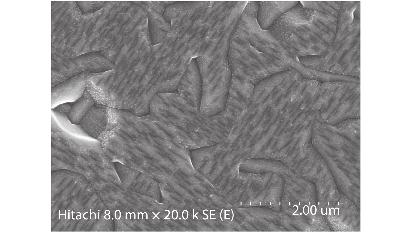
Fig. 1. Plane view SEM image of GaAs on Ge etched by melt KOH.
![(Color online) (a) TEM images of GaAs on Si with a Ge buffer. (b) and (c) show the Ge/Si interface and the GaAs/Ge interface, respectively[26].](/richHtml/jos/2019/40/10/101305/img_2.jpg)
Fig. 2. (Color online) (a) TEM images of GaAs on Si with a Ge buffer. (b) and (c) show the Ge/Si interface and the GaAs/Ge interface, respectively[26 ].
Fig. 3. (Color online) (a) CW PIV characteristics for an InAs QD laser on Si at 18 °C. (b) Emission spectrum for this device at various inject current density[31 ].
Fig. 4. (Color online) (a) The cross-sectional schematic diagram of the hybrid laser. The arrows marked with “+” and “−” show hole and electron flows, respectively. (b) Single-sided L –I –V characteristics of the hybrid BRS laser under continuous wave (CW) condition at room temperature. (c) The optical spectrum at 30 mA injection current with a 40 dB SMSR.
Fig. 5. (Color online) (a) ART technology silicon-based GaAs heteroepitaxial TEM image. (b) Lateral coverage epitaxial results. (c) Room temperature photoluminescence of GaAs grown on Si–GaAs substrate.
Fig. 6. (Color online) (a) Schematic diagram of growing GaAs. (b) SEM image of GaAs. (c) TEM image of GaAs.
Fig. 7. (Color online) (a) ART technology silicon-based InP growth SEM image in 2010. (b) Schematic diagram of the atomic step creation mechanism. (c) ART technology silicon-based V-groove InP growth SEM image in 2012. (d) High-resolution TEM image at Si and InP (111) interface.
Fig. 8. Silicon-based InGaAs/InP multiple quantum well structure and its photoluminescence spectrum at room temperature.
Fig. 9. (Color online) (a) Schematic diagram of a silicon-based InP DFB optical pump laser. (b) Cross-section electron micrograph of a silicon-based InP/InGaAs optical pump laser. (c) Cross-section electron micrograph of a silicon-based GaAs/InGaAs nanowire.
Fig. 10. (Color online) (a) Cross-sectional TEM image of one representative InP/InGaAs nanoridge on (001) Si. (b) Schematic of the transferred InP/InGaAs nanoridge on a SiO2/Si substrate. (c) Microscopic image and SEM of the transferred InP/InGaAs nanoridge. (d) PL spectra of the transferred InP/ InGaAs nanoridge under different excitation levels. (e) Emission spectra of the InP/InGaAs nanoridge at increasing excitation levels at 4.5 K.
Fig. 11. (Color online) (a) SEM image of III–V nanowires on the SOI substrate. (b) SEM images of III–V nanowires on the SOI substrate after etching. (c) The FDTD simulation results of a III–V nanowire on the SOI substrate after etching.


Set citation alerts for the article
Please enter your email address

© Copyright 2018-2021 | Chinese Laser Press. All Rights Reserved 沪ICP备15018463号-20