
Wenyu Yang, Yajie Li, Fangyuan Meng, Hongyan Yu, Mengqi Wang, Pengfei Wang, Guangzhen Luo, Xuliang Zhou, Jiaoqing Pan. III–V compound materials and lasers on silicon[J]. Journal of Semiconductors, 2019, 40(10): 101305
- Journal of Semiconductors
- Vol. 40, Issue 10, 101305 (2019)
Abstract
1. Introduction
Over the past half century, technological innovation and industrial revolution represented by microelectronics technology and integrated circuits have led the world into a highly informational, networked and intelligent era. Microelectronic devices have laid the foundation for the rapid development of society. At the same time, higher requirements for the performance of microelectronic devices and integrated circuits have been proposed to meet the needs for a larger amount of information acquisition and processing. However, conventional silicon integrated circuits have become increasingly unable to meet increasing demands in terms of data processing speed and bandwidth performance. For decades, people have been working to improve the integration of microelectronics chips to solve related problems, but the average cost per chip is still high on each wafer. Several physical effects[
In order to solve the above problems, people have turned their attention to photonics, and use photons as a carrier for information processing and transmission[
Considering the compatibility with CMOS processes, it is a general trend to manufacture and integrate various photonic devices on silicon. Here we review three main methods of integration of III–V materials on Si, namely direct growth, bonding, and selective-area hetero-epitaxy. The III–V materials we introduce mainly include materials such as GaAs and InP. The lasers are mainly lasers of related communication bands. We also introduced the advantages and challenges of the three growth methods.
2. Methods of integration of III–V materials on Si
2.1. Direct growth of III–V materials on Si
The direct growth of III–V compound semiconductors on silicon is the first attempt[
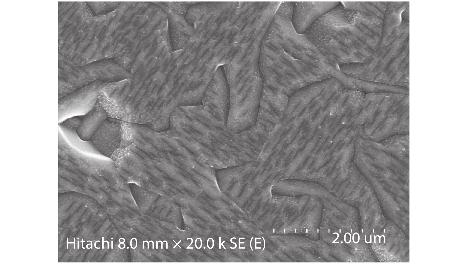
![]()
Figure 1.Plane view SEM image of GaAs on Ge etched by melt KOH.
The GaAs-based material system is the most studied III–V compound on Si because of its wide usage and relatively smaller lattice mismatch compared with InP-based materials. To solve the mismatch problem such as InGaAs interlayer[
![]()
Figure 2.(Color online) (a) TEM images of GaAs on Si with a Ge buffer. (b) and (c) show the Ge/Si interface and the GaAs/Ge interface, respectively[
Although much effort has been made, there are no practical devices that have been fabricated on the GaAs/Si platform, because the lowest defect density for the GaAs top layer could reach only 105–106 cm–2[
Although it is difficult to achieve high performance devices on III–V/Si material system, research has not been suspended, especially lasers on Si. Due to proper band structure, III–V materials are grown on Si for light source emitting at fiber-optic communication wavelength. From the 1980s, GaAs/AlGaAs[
InAs quantum dot (QD) lasers operating at 1.3 μm have recently been grown on miscut Ge[
![]()
Figure 3.(Color online) (a) CW PIV characteristics for an InAs QD laser on Si at 18 °C. (b) Emission spectrum for this device at various inject current density[
In short, the research on silicon-based large-area epitaxial III–V semiconductors has been carried out very early, and material defects have not been completely solved. In addition, the laser fabricated by this method still needs to grow a thick buffer layer between the III–V semiconductor and the silicon substrate, and the defect density in the buffer layer is relatively large, which greatly reduces the coupling efficiency and device lifetime at elevated temperature, respectively. Silicon-based quantum dot lasers have made great progress, but the gain is still relatively low. Therefore, there is a limitation in the large-scale integration of light sources on silicon by the conventional buffer layer epitaxial III–V semiconductor material method.
2.2. Silicon-based bonded lasers
In the current situation, bonding is a very practical method[
Direct bonding does not require any medium, and directly bonds two substrates with atomic level flat surfaces together using heat and pressure[
Adhesive bonding mainly uses some high molecular organic materials as a bonding material to bond the chip and the wafer. Commonly used bonding materials are mainly benzocyclobutene (BCB), photoresist and polyimide. The adhesive bonding process is simple, the bonding temperature is low, the requirement for surface flatness is relatively low, and the bonding strength is high. However, the main problem is that the organic material used for bonding has poor electrical and thermal conductivity. Ghent University, in conjunction with several organizations, produced a hybrid integrated silicon-based DFB laser using an ultra-thin BCB bonding layer[
Metal bonding refers to the bonding of two wafers or devices by means of a pure metal or alloy, by metal bonding, metal melting or diffusion between metal and wafer. Its main advantages are superior electrical performance, high reliability, good thermal conductivity, and effective release of stress. Andrijasevic et al. used Au–Au hot pressing to bond a GaAs-based quantum cascade laser to a silicon substrate at a bonding temperature of 330 °C[
![]()
Figure 4.(Color online) (a) The cross-sectional schematic diagram of the hybrid laser. The arrows marked with “+” and “−” show hole and electron flows, respectively. (b) Single-sided
In short, bonding is a very practical method so far. At the same time, bonding is a relatively mature method, and there are already some applications in the business such as Intel and Juniper Network. It can be used to effectively solve the excessive defect density caused by growing III–V materials on silicon and to integrate light sources on silicon for large scale commercialization.
2.3. Selective-area hetero-epitaxy
Selective-area hetero-epitaxy, which is an epitaxial method that restricts epitaxial materials in the pre-defined regions[
The selective-area hetero-epitaxy technique was used in the heteroepitaxial epitaxy of silicon-based III–V materials[
![]()
Figure 5.(Color online) (a) ART technology silicon-based GaAs heteroepitaxial TEM image. (b) Lateral coverage epitaxial results. (c) Room temperature photoluminescence of GaAs grown on Si–GaAs substrate.
To better limit defects, researchers have applied V-grooves to grow materials. Researchers have successfully used MOCVD to epitaxially produce high-quality GaAs materials on Si (001) substrates[
![]()
Figure 6.(Color online) (a) Schematic diagram of growing GaAs. (b) SEM image of GaAs. (c) TEM image of GaAs.
In order to expand the range of applications of the materials, researchers have also developed InP-based materials, a material that can be used to emit light in the telecom wavelengths. In 2010, researchers at IMEC successfully grew InP materials on Si substrates by growing a thin layer of Ge buffer layer and SiO2 trench isolation to suppress dislocations[
![]()
Figure 8.Silicon-based InGaAs/InP multiple quantum well structure and its photoluminescence spectrum at room temperature.
To achieve the communication band, researchers have grown some quantum well materials like InGaAs/InP multiple quantum wells. The researchers epitaxially grew high-quality InP materials on this basis. To realize silicon-based high gain laser materials the InGaAs/InP multiple quantum well structure was successfully epitaxially grown on InP materials[
![]()
Figure 10.(Color online) (a) Cross-sectional TEM image of one representative InP/InGaAs nanoridge on (001) Si. (b) Schematic of the transferred InP/InGaAs nanoridge on a SiO2/Si substrate. (c) Microscopic image and SEM of the transferred InP/InGaAs nanoridge. (d) PL spectra of the transferred InP/ InGaAs nanoridge under different excitation levels. (e) Emission spectra of the InP/InGaAs nanoridge at increasing excitation levels at 4.5 K.
Researchers have carried out many experiments and used many methods in order to achieve light pump illumination. The research team at Gent University and IMEC in Belgium has done a lot of research in this area. They used the ART method to directly grow high-quality InP nanowires outside the Si substrate with periodic V-grooves and SiO2 sidewalls and fabricated DFB laser arrays in 2015. They achieved light pump lasing at room temperature. Since the gain material is only InP, its lasing wavelength is about 920 nm[
Researchers at the Hong Kong University of Science and Technology used another way to achieve the light pump. They grew InP/InGaAs nanoridges on Si substrates, transferring InP/InGaAs nanoridges onto SiO2/Si substrates, and observed the Fabry-Perot resonance mode at room temperature, and achieving 1400 nm multimode lasing behavior under continuous wave optical pumping at 4.5 K[
In previous studies, researchers found that the refractive index of silicon is larger than that of III–V materials such as InP, GaAs, and InGaAs. The light field generated by the III–V material will continuously leak into the silicon substrate, so it cannot form the guided wave mode that can propagate, and it cannot form a resonant cavity. In 2019, the researchers found that after removing the silicon around the III–V nanowires (bottom), the entire III–V nanowires were wrapped in air, and the refractive index of the air was approximately 1, which was much smaller than the III–V material. This structure has a good limit on light and can form a guided wave mode to provide optical gain[
ART technology is still in the laboratory stage, and there is still a long way to go for large-scale applications. The materials grown by ART technology are now only optically pumped[
3. Conclusion
III–V compound materials and lasers on Si substrates is a rapidly evolving research field with tremendous potential. Direct epitaxial quantum dot lasers have been able to electrically pump lasers at room temperature. Bonded lasers have already been put into commercial use. High quality III–V compound materials can be grown with ART technology. These all show the possibility of combining with traditional CMOS technology, which can be used to make high-speed communication networks in the future.
Acknowledgments
This work was supported by the National Key Technology R&D Program (Grant No. 2018YFA0209001) and Frontier Science Research Project of CAS (Grant No. QYZDY-SSW-JSC021).
References
[1] S Kim, M Yokoyama, N Taoka et al. Self-aligned metal source/drain In
[2]
[3] C G Lee, X D Wang, J W Kysar et al. Measurement of the elastic properties and intrinsic strength of monolayer graphene. Science, 321, 385(2008).
[4] A K Geim, K S Novoselov. The rise of graphene. Nat Mater, 6, 183(2009).
[5]
[6] V R Almeida, C A Barrios, R R Panepucci et al. All-optical control of light on a silicon chip. Nature, 431, 1081(2004).
[7] J Michel, J Liu, L C Kimerling. High-performance Ge-on-Si photodetectors. Nat Photonics, 4, 527(2000).
[8] C Sun, M T Wade, Y Lee et al. Single-chip microprocessor that communicates directly using light. Nature, 528, 534(2015).
[9] Y Vlasov, W M J Green, F J Xia. High-throughput silicon nanophotonic wavelength-insensitive switch for on-chip optical networks. Nat Photonics, 2, 1(2008).
[10]
[11] R Won, M J Paniccia. Integrating silicon photonics. Nat Photonics, 4, 498(2010).
[12] L Andrew, J Qi, T Mingchu et al. Continuous-wave InAs/GaAs quantum-dot laser diodes monolithically grown on Si substrate with low threshold current densities. Opt Express, 20, 22181(2012).
[13] R D Bringans, D K Biegelsen, L Swartz. Atomic-step rearrangement on Si(100) by interaction with arsenic and the implication for GaAs-on-Si epitaxy. Phys Rev, 44, 3054(1991).
[14]
[15] H Mori, M Tachikawa, M Sugo et al. GaAs heteroepitaxy on an epitaxial Si surface with a low-temperature process. Appl Phys Lett, 63, 1963(1993).
[16] S Sakai, T Soga, M Takeyasu et al. Room-temperature laser operation of AlGaAs/GaAs double heterostructures fabricated on Si substrates by metalorganic chemical vapor deposition. Appl Phys Lett, 48, 413(1986).
[17]
[18] S M Ting, E A Fitzgerald. Metal-organic chemical vapor deposition of single domain GaAs on Ge/Ge
[19] T H Windhorn, G M Metze, B Y Tsaur et al. AlGaAs double-heterostructure diode lasers fabricated on a monolithic GaAs/Si substrate. Appl Phys Lett, 45, 309(1984).
[20] Y Takano, M Hisaka, N Fujii et al. Reduction of threading dislocations by InGaAs interlayer in GaAs layers grown on Si substrates. Appl Phys Lett, 73, 2917(1998).
[21] K Asai, H Katahama, Y Shiba. Dynamical formation process of pure edge misfit dislocations at GaAs/Si interfaces in post-annealing. J Appl Phys, 33, 4843(1994).
[22] Y Takagi, H Yonezu, Y Hachiya et al. Reduction mechanism of threading dislocation density in GaAs epilayer grown on Si substrate by high-temperature annealing. Jpn J Appl Phys, 33, 3368(1994).
[23] Y Kohama, Y Kadota, Y Ohmachi. InP grown on Si substrates with GaP buffer layers by metalorganic chemical vapor deposition. Jpn J Appl Phys, 28, 1337(1989).
[24] R Fischer, W Kopp, H Morkoc et al. Low threshold laser operation at room temperature in GaAs/(Al, Ga)As structures grown directly on (100)Si. Appl Phys Lett, 48, 1360(1986).
[25] X L Zhou, J Q Pan, R R Liang et al. Epitaxy of GaAs thin film with low defect density and smooth surface on Si substrate. J Semicond, 35, 073002(2014).
[26] Y Li, L J Giling. A closer study on the self-annihilation of antiphase boundaries in GaAs epilayers. J Cryst Growth, 163, 203(1996).
[27] M Tang, S Chen, J Wu et al. 1.3-
[28] M Sugo, H Mori, Y Sakai et al. Stable cw operation at room temperature of a 1.5-
[29] H Liu, T Wang, J Qi et al. Long-wavelength InAs/GaAs quantum-dot laser diode monolithically grown on Ge substrate. Nat Photonics, 5, 416(2011).
[30] S Chen, W Li, J Wu et al. Electrically pumped continuous-wave III–V quantum dot lasers on silicon. Nat Photonics, 10, 307(2016).
[31] K Jinkwan, J Bongyong, L Joohang et al. All MBE grown InAs/GaAs quantum dot lasers on on-axis Si (001). Opt Express, 26, 11568(2018).
[32] J C Norman, D Jung, Z Zhang et al. A review of high-performance quantum dot lasers on silicon. IEEE J Quantum Electron, 55, 1(2019).
[33] D Jung, R Herrick, J Norman et al. Impact of threading dislocation density on the lifetime of InAs quantum dot lasers on Si. Appl Phys Lett, 112, 153507(2018).
[34] A Y Liu, Y C Zhang, J Norman et al. High performance continuous wave 1.3
[35] S Zhu, B Shi, Q Li et al. 1.5
[36] Y Wan, L Qiang, A Y Liu et al. Sub-wavelength InAs quantum dot micro-disk lasers epitaxially grown on exact Si (001) substrates. Appl Phys Lett, 108, 1(2016).
[37] J Norman, M J Kennedy, J Selvidge et al. Electrically pumped continuous wave quantum dot lasers epitaxially grown on patterned, on-axis (001) Si. Opt Express, 25, 3927(2017).
[38] J Isenberg, W J Warta. Free carrier absorption in heavily doped silicon layers. Appl Phys Lett, 84, 2265(2004).
[39] A V Krishnamoorthy, L M F Chirovsky, W S Hobson et al. Vertical-cavity surface-emitting lasers flip-chip bonded to gigabit-per-second CMOS circuits. IEEE Photonics Technol Lett, 11, 128(1999).
[40] A W Fang, L Erica, Y H Kuo et al. A distributed feedback silicon evanescent laser. Opt Express, 16, 4413(2008).
[41] A W Fang, P Hyundai, C Oded et al. Electrically pumped hybrid AlGaInAs-silicon evanescent laser. Opt Express, 14, 9203(2006).
[42] A W Fang, B R Koch, R Jones et al. A distributed Bragg reflector silicon evanescent laser. IEEE Photonics Technol Lett, 20, 1667(2008).
[43] A D Groote, P Cardile, A Z Subramanian et al. Transfer-printing-based integration of single-mode waveguide-coupled III–V-on-silicon broadband light emitters. Opt Express, 24, 13754(2016).
[44] P F Hyundai, F K Alexander, K Satoshi et al. Hybrid silicon evanescent laser fabricated with a silicon waveguide and III–V offset quantum wells. Opt Express, 13, 9460(2005).
[45] J Justice, C Bower, M Meitl et al. Wafer-scale integration of group III–V lasers on silicon using transfer printing of epitaxial layers. Nat Photonics, 6, 612(2012).
[46] D Pasquariello, K J Hjort. Plasma-assisted InP-to-Si low temperature wafer bonding. IEEE J Sel Top Quantum Electron, 8, 118(2002).
[47] S Keyvaninia, S Verstuyft, L Van Landschoot et al. Heterogeneously integrated III–V/silicon distributed feedback lasers. Opt Lett, 38, 5434(2013).
[48] S Sui, M T Tang, Y Yang et al. Sixteen-wavelength hybrid AlGaInAs/Si microdisk laser array. IEEE J Quantum Electron, 51, 2600108(2015).
[49] D Andrijasevic, M Austerer, A M Andrews et al. Hybrid integration of GaAs quantum cascade lasers with Si substrates by thermocompression bonding. Appl Phys Lett, 92, 157(2008).
[50] L Yuan, L Tao, H Yu et al. Hybrid InGaAsP-Si evanescent laser by selective-area metal-bonding method. IEEE Photonics Technol Lett, 25, 1180(2013).
[51] L Yuan, L Tao, W Chen et al. A buried ridge stripe structure InGaAsP-Si hybrid laser. IEEE Photonics Technol Lett, 27, 352(2015).
[52] T Hong, Y Wang, H Y Yu et al. A Selective area metal bonding method for Si photonics light sources. IEEE International Conference on Group IV Photonics(2010).
[53] H Yu, L Yuan, L Tao et al. 1550 nm evanescent hybrid InGaAsP-Si laser with buried ridge stripe structure. IEEE Photonics Technol Lett, 28, 1146(2016).
[54] T A Langdo, C W Leitz, M T Currie et al. High quality Ge on Si by epitaxial necking. Appl Phys Lett, 76, 3700(2000).
[55] Q Li, S M Han, S R J Brueck et al. Selective growth of Ge on Si(100) through vias of SiO2 nanotemplate using solid source molecular beam epitaxy. Appl Phys Lett, 83, 5032(2003).
[56] R J Matyi, H Shichijo, H L Tsai et al. Patterned growth of gallium arsenide on silicon. J Vac Sci Technol B, 6, 699(1988).
[57] K Woodbridge, P Barnes, R Murray et al. GaAs / AlGaAs pin MQW structures grown on patterned Si substrates. J Cryst Growth, 127, 112(1993).
[58] J S Park, J Bai, M Curtin et al. Defect reduction of selective Ge epitaxy in trenches on Si(001) substrates using aspect ratio trapping. Appl Phys Lett, 90, 3344(2007).
[59] J Z Li, J Bai, J S Park et al. Defect reduction of GaAs epitaxy on Si (001) using selective aspect ratio trapping. Appl Phys Lett, 91, 2293(2007).
[60] S Li, X Zhou, X Kong et al. Evaluation of growth mode and optimization of growth parameters for GaAs epitaxy in V-shaped. J Cryst Growth, 426, 147(2015).
[61] S Y Li, X L Zhou, X T Kong et al. Selective area growth of GaAs in V-grooved trenches on Si (001) substrates by aspect-ratio. Chin Phys Lett, 32, 028101(2015).
[62] G Wang, M R Leys, R Loo et al. Selective area growth of high quality InP on Si (001) substrates. Appl Phys Lett, 97, 1(2010).
[63] M Paladugu, C Merckling, R Loo et al. Site selective integration of III–V materials on Si for nanoscale logic and photonic devices. Cryst Growth Des, 12, 4696(2012).
[64] S Li, X Zhou, X Kong et al. Catalyst-free growth of InP nanowires on patterned Si (001) substrate by using GaAs buffer layer. J Cryst Growth, 440, 81(2016).
[65] S Li, X Zhou, M Li et al. Ridge InGaAs/InP multi-quantum-well selective growth in nanoscale trenches on Si (001) substrate. Appl Phys Lett, 108, 021902(2016).
[66] Z Wang, B Tian, M Pantouvaki et al. Room-temperature InP distributed feedback laser array directly grown on silicon. Nat Photonics, 9, 837(2015).
[67] B Tian, C Merckling, D V Thourhout et al. Room temperature InGaAs/InP distributed feedback laser directly grown on silicon. Lasers & Electro-optics(2016).
[68] B Kunert, W Guo, Y Mols et al. III/V nano ridge structures for optical applications on patterned 300 mm silicon substrate. Appl Phys Lett, 109, 511(2016).
[69] Y Han, Q Li, u S Zhu et al. Continuous-wave lasing from InP/InGaAs nanoridges at telecommunication wavelengths. Appl Phys Lett, 111, 212101(2017).
[70] Y Li, M Wang, X Zhou et al. InGaAs/InP multi-quantum-well nanowires with a lower optical leakage loss on V-groove-patterned SOI substrates. Opt Express, 27, 494(2019).
[71] Y Han, W K Ng, Y Xue et al. Telecom InP/InGaAs nanolaser array directly grown on (001) silicon-on-insulator. Opt Lett, 44, 767(2019).


Set citation alerts for the article
Please enter your email address

© Copyright 2018-2021 | Chinese Laser Press. All Rights Reserved 沪ICP备15018463号-20