• Photonics Research
  • Vol. 5, Issue 6, 702 (2017)
Yiding Lin1、2、3, Kwang Hong Lee2, Shuyu Bao1、2, Xin Guo1, Hong Wang1, Jurgen Michel2、4, and Chuan Seng Tan1、2、*
Author Affiliations
  • 1School of Electrical and Electronic Engineering, Nanyang Technological University, Singapore 639798, Singapore
  • 2Low Energy Electronic Systems (LEES), Singapore-MIT Alliance for Research and Technology, Singapore 138602, Singapore
  • 3e-mail: liny0075@e.ntu.edu.sg
  • 4Department of Materials Science and Engineering, Massachusetts Institute of Technology, Cambridge, Massachusetts 02139, USA
  • show less
    DOI: 10.1364/PRJ.5.000702 Cite this Article Set citation alerts
    Yiding Lin, Kwang Hong Lee, Shuyu Bao, Xin Guo, Hong Wang, Jurgen Michel, Chuan Seng Tan. High-efficiency normal-incidence vertical p-i-n photodetectors on a germanium-on-insulator platform[J]. Photonics Research, 2017, 5(6): 702 Copy Citation Text show less
    Schematic of bonding and layer transfer technique for GOI p-i-n structure fabrication.
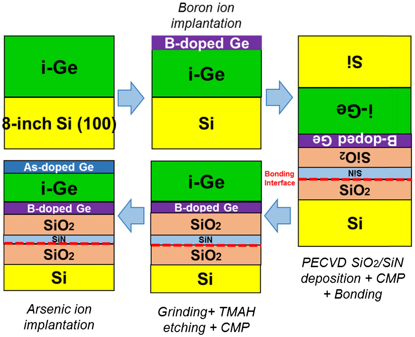
    Fig. 1. Schematic of bonding and layer transfer technique for GOI p-i-n structure fabrication.
    (a) SIMS doping profiles of B and As in Ge vertical p-i-n structure. Inset shows a corresponding cross-sectional TEM image of the fabricated GOI p-i-n structure at bonding interface. (b) HRXRD (004) 2θ−ω scan of as-grown Ge-on-Si and GOI p-i-n structure with that of bulk Ge as reference. Tensile strain of ∼0.15% for the Ge layer in the GOI was obtained. The values in the plot correspond to the respective peak 2θ−ω angles.
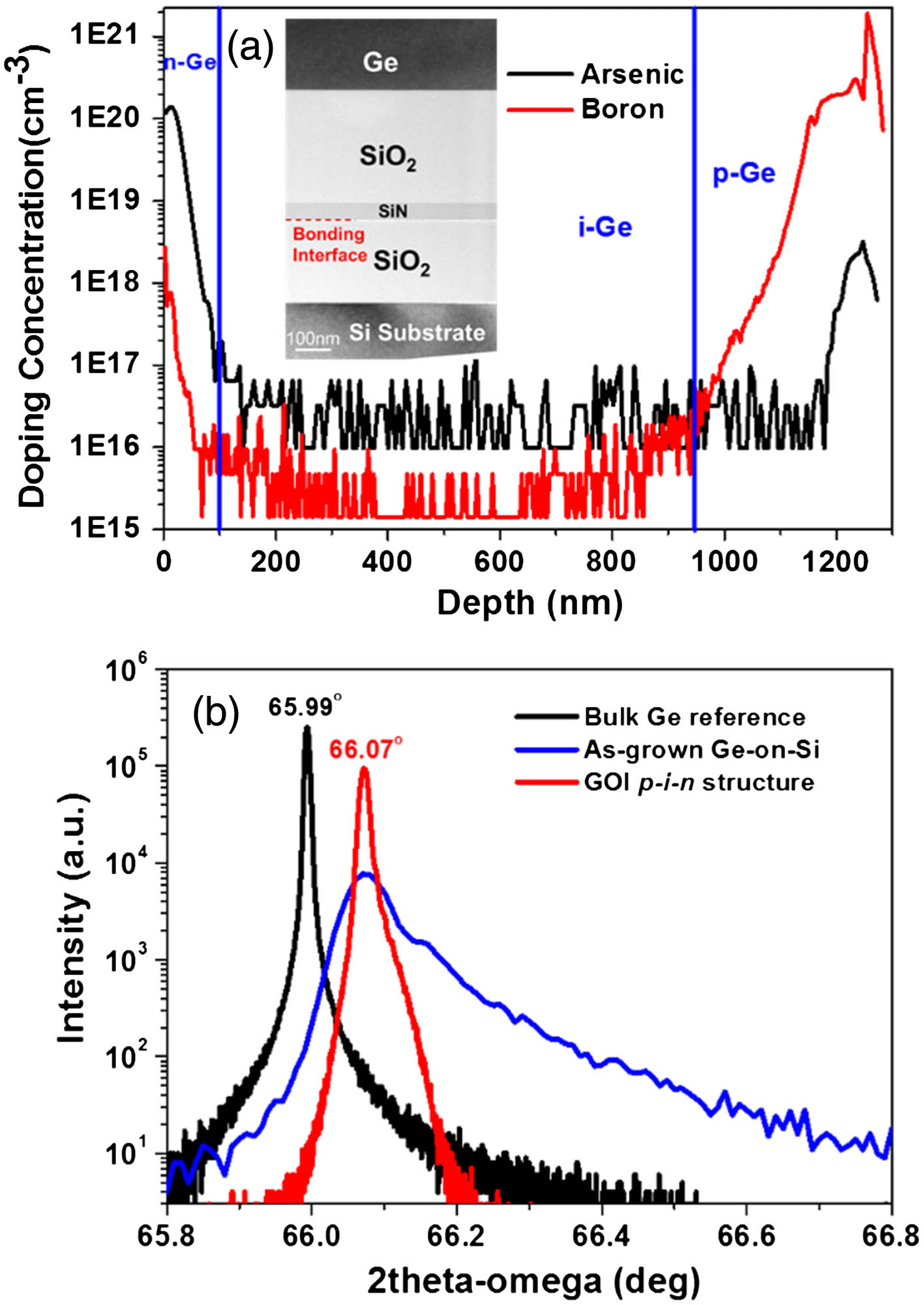
    Fig. 2. (a) SIMS doping profiles of B and As in Ge vertical p-i-n structure. Inset shows a corresponding cross-sectional TEM image of the fabricated GOI p-i-n structure at bonding interface. (b) HRXRD (004) 2θω scan of as-grown Ge-on-Si and GOI p-i-n structure with that of bulk Ge as reference. Tensile strain of 0.15% for the Ge layer in the GOI was obtained. The values in the plot correspond to the respective peak 2θω angles.
    (a) Cross-sectional schematic of a GOI vertical p-i-n photodetector (PD) and (b) its optical microscope image with a mesa diameter of 80 μm. The FESEM image above presents the cross-sectional view of the detector along the green solid line across the mesa.
    Fig. 3. (a) Cross-sectional schematic of a GOI vertical p-i-n photodetector (PD) and (b) its optical microscope image with a mesa diameter of 80 μm. The FESEM image above presents the cross-sectional view of the detector along the green solid line across the mesa.
    (a) Dark current density-voltage characteristic of GOI vertical p-i-n PDs with different mesa diameters. (b) Temperature-dependent study on dark current of GOI vertical p-i-n PD at −0.5 V.
    Fig. 4. (a) Dark current density-voltage characteristic of GOI vertical p-i-n PDs with different mesa diameters. (b) Temperature-dependent study on dark current of GOI vertical p-i-n PD at 0.5  V.
    (a) Photocurrent of a GOI vertical p-i-n PD (mesa diameter of 250 μm) as a function of applied bias, with its dark I-V characteristic as a reference. Inset shows the corresponding measurement configuration. (b) Optical responsivity spectrum of GOI vertical p-i-n PD across C- and L- telecommunication bands. Inset shows the corresponding first-order derivative of the responsivity spectrum.
    Fig. 5. (a) Photocurrent of a GOI vertical p-i-n PD (mesa diameter of 250 μm) as a function of applied bias, with its dark I-V characteristic as a reference. Inset shows the corresponding measurement configuration. (b) Optical responsivity spectrum of GOI vertical p-i-n PD across C- and L- telecommunication bands. Inset shows the corresponding first-order derivative of the responsivity spectrum.
    Performance comparison of Ge-based PDs. i-Ge thicknesses for the corresponding Ge-on-Si and Ge-on-SOI devices (without AR coating) in the references (numbers in square brackets) were indicated. The i-Ge thicknesses for GOI PDs were not indicated due to their discrepant configurations (interdigitated lateral p-i-n [19] and waveguide-integrated [21]).
    Fig. 6. Performance comparison of Ge-based PDs. i-Ge thicknesses for the corresponding Ge-on-Si and Ge-on-SOI devices (without AR coating) in the references (numbers in square brackets) were indicated. The i-Ge thicknesses for GOI PDs were not indicated due to their discrepant configurations (interdigitated lateral p-i-n [19] and waveguide-integrated [21]).
    (a) Frequency response of GOI vertical p-i-n PD (mesa diameter of 60 μm) at −2 V. Inset shows device series resistance extracted from I-V characteristics. (b) Calculated 3 dB bandwidth of GOI vertical p-i-n detector (Rs=30 Ω) with respect to its mesa diameter (red solid line). The dashed line represents the corresponding carrier transit-limited bandwidth. Inset shows linear interpolation of device capacitances at −2 V for de-coupling of junction and parasitic capacitances. (c) Calculated 3 dB bandwidth of the PD with mesa diameter of 10 μm with respect to i-Ge thickness.
    Fig. 7. (a) Frequency response of GOI vertical p-i-n PD (mesa diameter of 60 μm) at 2  V. Inset shows device series resistance extracted from I-V characteristics. (b) Calculated 3 dB bandwidth of GOI vertical p-i-n detector (Rs=30Ω) with respect to its mesa diameter (red solid line). The dashed line represents the corresponding carrier transit-limited bandwidth. Inset shows linear interpolation of device capacitances at 2  V for de-coupling of junction and parasitic capacitances. (c) Calculated 3 dB bandwidth of the PD with mesa diameter of 10 μm with respect to i-Ge thickness.
    Yiding Lin, Kwang Hong Lee, Shuyu Bao, Xin Guo, Hong Wang, Jurgen Michel, Chuan Seng Tan. High-efficiency normal-incidence vertical p-i-n photodetectors on a germanium-on-insulator platform[J]. Photonics Research, 2017, 5(6): 702
    Download Citation