In this paper, normal incidence vertical p-i-n photodetectors on a germanium-on-insulator (GOI) platform were demonstrated. The vertical p-i-n structure was realized by ion-implanting boron and arsenic at the bottom and top of the Ge layer, respectively, during the GOI fabrication. Abrupt doping profiles were verified in the transferred high-quality Ge layer. The photodetectors exhibit a dark current density of ~47 mA/cm2 at ?1 V and an optical responsivity of 0.39 A/W at 1550 nm, which are improved compared with state-of-the-art demonstrated GOI photodetectors. An internal quantum efficiency of ~97% indicates excellent carrier collection efficiency of the device. The photodetectors with mesa diameter of 60 μm exhibit a 3 dB bandwidth of ~1 GHz, which agrees well with theoretical calculations. The bandwidth is expected to improve to ~32 GHz with mesa diameter of 10 μm. This work could be similarly extended to GOI platforms with other intermediate layers and potentially enrich the functional diversity of GOI for near-infrared sensing and communication integrated with Ge CMOS and mid-infrared photonics.
Germanium (Ge) has been extensively studied in past decades for diversified electronics and photonics applications on the silicon (Si)-based CMOS integrated circuit (IC) platform, owing to its process compatibility for monolithic integration. As conventional miniaturization of transistors encounters difficulty in extending Moore’s law, Ge, thanks to its higher mobility and lower effective mass of carriers, was adopted to replace Si as transistor channel material for larger drive current and faster ICs with down-scaled supply voltage [1]. On the other hand, Ge exhibits considerable optical absorption into C- and L-telecommunication bands, which facilitates the development of on-chip optical interconnects [2,3] for fiber-optic communication. Numerous reports have been released on Ge-based photodetectors [4], modulators [5], and lasers [6,7]. In addition, high refractive index as well as optical transparency of Ge in the mid-infrared (mid-IR) regime (2–15 μm) attracts the attention of researchers for on-chip molecule sensing and mid-IR communication [8,9]. Therefore, the Ge/CMOS platform is envisioned to be suitable for many novel electronic–photonic integrated applications across a wide spectrum range.
In recent years, a germanium-on-insulator (GOI) has been under active research as one of the potential platforms for future Ge-based CMOS electronic and photonic applications [10–12]. The insertion of an insulator layer between Ge and Si provides a number of advantages. First, the “on-insulator” substrate benefits the electrostatic control of Ge CMOS such as suppressed short channel effects and reduced parasitic capacitance [13]. Second, the insulator layer (e.g., and sapphire) beneath Ge waveguides could provide larger core-clad index contrast for better optical confinement, enabling more compact and sensitive on-chip sensors at the mid-IR region [14]. Furthermore, selection of the insulator material can be quite flexible based on specific needs. For example, high- dielectrics (e.g., and ) could be adopted for continuing downscaling of transistors with improved Ge/oxide interface [15,16]; chalcogenide glass could also be utilized to support the entire mid-IR photonics applications [17].
Although the GOI platform has shown superior adaptability for mid-IR sensing and high-performance CMOS electronics, it is rarely explored for optoelectronics in the near-IR region, while great achievement has been established on conventional Ge-on-Si and Ge-on-SOI as monolithically integrated fiber-optic communication platforms, attributing to their Si waveguides directly in contact with Ge for efficient coupling. The GOI platform, due to the lack of suitable inherent waveguide and cladding, is challenging to be directly applied for on-chip optical interconnects. However, discrete optoelectronic devices could still be developed on GOI to enrich the functionality of the platform, with photodetectors [18–21], free-carrier absorption modulator [22], and engineered highly strained structures potentially for lasers [23,24] demonstrated. Most of these demonstrated photodetectors are with an inter-digitated configuration [18–20]. This configuration is simple process-wise, but the device responsivity and speed might be mutually compromised by inter-digitated finger width and spacing. Chen et al.[21] also reported a waveguide-integrated photodiode on GOI-on-SOI platform via wafer bonding. However, the bonding interfacial insulator layer must be kept thin for efficient optical coupling into the detector, which tends to limit the versatility of the platform as well as the wafer-scale bonding quality, since Bao et al.[25] recently observed GOI bonding quality degradation with thin intermediate thermal oxide.
Sign up for Photonics Research TOC. Get the latest issue of Photonics Research delivered right to you!Sign up now
Therefore, in this work, we demonstrate normal incidence vertical photodetectors developed on germanium-on--insulator substrate. The vertical structure was realized via ion-implantation of boron (B) and arsenic (As) at the bottom and top of the Ge layer, respectively, during bonding and layer transfer process in the GOI fabrication. With the -contact being introduced at the bottom of the Ge layer, photon-generated carriers could be collected more efficiently via the vertical electric field to enhance the responsivity, compared with the inter-digitated device configuration. The device fabrication technique is also expected to be compatible with GOI platforms with different intermediate materials, demonstrating its excellent potential contributing to GOI-based CMOS-photonics platform for plentiful applications such as on-chip optical receivers or near-IR LiDAR systems integrated with novel high-speed Ge electronics and mid-IR photonics.
2. GOI VERTICAL p-i-n STRUCTURE
A. Experimental
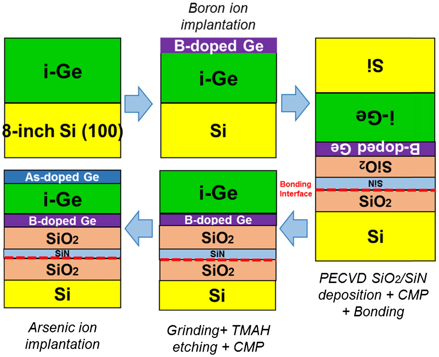
The fabrication of a GOI vertical structure is similar to that previously reported [26,27], as shown in Fig. 1. An intrinsic Ge (-Ge) layer was epitaxial-grown on a 200 mm Si (100) carrier wafer, followed by B ion implantation to form a -Ge layer. An interfacial layer was deposited via plasma-enhanced chemical vapor deposition (PECVD) on both Ge and the other Si handle wafer. A SiN layer was then deposited by PECVD on the Ge-on-Si wafer to help with suppressing interfacial void formation during the latter bonding stage. Prior to bonding, both dielectric surfaces were treated under plasma for 15 s, followed by deionized water rinsing and spin drying. After the surface treatment, the Ge-on-Si wafer was flipped over and bonded to the Si handle wafer at room temperature followed by annealing at 300°C for 3 h in ambient to enhance the bonding strength. Grinding, tetramethylammonium hydroxide (TMAH) etching, and then chemical-mechanical polishing (CMP) were implemented to remove the Si carrier wafer and defective Ge. As implantation was then performed to form the -layer in Ge. Dopant activation was performed at 650°C for 15 s by rapid thermal annealing (RTA) to minimize dopant diffusion.
Figure 1.Schematic of bonding and layer transfer technique for GOI structure fabrication.
The fabricated GOI structure was systematically characterized by the techniques described below. Cameca IMS secondary ion mass spectrometry (SIMS) was used to analyze the B and As doping profiles in Ge. Transmission electron microscopy (TEM) was utilized to evaluate the GOI bonding quality at cross-sectional view. High-resolution X-ray diffraction (HRXRD) study was performed by using a PANalytical X’Pert PRO X-ray diffractometer to determine film quality and residual strain of Ge before and after bonding and layer transfer.
B. Results and Discussion
Figure 2(a) shows the doping profiles of B and As with respect to the depth in the Ge layer. Both the B and As profiles reveal abrupt concentration interfaces at and 1100 nm depth, respectively, with low concentration below the detection limit at the intrinsic region. This confirms minimal diffusion of B and As dopants in maintaining the -Ge thickness for sufficient optical absorption. Due to the layer transfer technique, the ion implantation approach becomes viable to introduce both - and -Ge layers, which eliminates the concern of excess diffusion of in situ introduced dopants during Ge growth and cyclic annealing [28]. The inset shows a cross-sectional TEM image at the bonding interface of the realized GOI vertical structure. A seamless and void-free bonding interface was observed, implying high quality of bonding and layer transfer process. Figure 2(b) depicts the HRXRD (004) scan results of the as-grown Ge-on-Si and the GOI vertical structure, with that of bulk Ge wafer as a reference. It can be observed that the Ge peak intensity increases (by an order of magnitude) and the peak FWHM decreases (from 227 to 48 arcsec) from the as-grown film to GOI, indicating improved Ge film quality after bonding and layer transfer. This is due to the removal of the highly defective Ge layer close to the Ge/Si interface during the CMP process, which is also verified by the minimized shoulder at right-side of the GOI HRXRD peak toward higher angles, which has been correlated with Si/Ge inter-diffusion during the Ge-on-Si growth [26]. The residual strain in the Ge film, due to thermal expansion coefficient mismatch between Ge and Si, was calculated based on the Ge lattice constants obtained from the HRXRD peak angles of GOI and bulk Ge, as illustrated in Ref. [26]. It was found that tensile strain remained in the Ge film, which is close to the reported values [18,29]. The tensile strain also serves as an important guide in understanding the optical responsivity spectrum of the GOI photodetector at a later part of the study.
Figure 2.(a) SIMS doping profiles of B and As in Ge vertical structure. Inset shows a corresponding cross-sectional TEM image of the fabricated GOI structure at bonding interface. (b) HRXRD (004) scan of as-grown Ge-on-Si and GOI structure with that of bulk Ge as reference. Tensile strain of for the Ge layer in the GOI was obtained. The values in the plot correspond to the respective peak angles.
The realized GOI vertical structure was further developed into photodetectors with its cross-sectional schematic, as shown in Fig. 3(a). First, optical lithography patterning followed by reactive-ion etching (RIE) were repetitively performed on the GOI vertical structure to form both - and -Ge regions. was then deposited using PECVD as a device passivation layer. Afterward, ring-shaped trenches were created on both - and -Ge regions to define metal/Ge contact areas, followed by sputtering and lift-off of a Ti/TiN/Al metal stack to form device metal/Ge contacts. RTA at 400°C for 1 min was implemented to enhance the ohmic characteristic of the contacts. Figure 3(b) shows the optical microscope image of a fabricated photodetector with a mesa diameter of 80 μm. The image reveals clear device surface features of the mesa regions and metal pads. The field emission scanning electron microscope (FESEM) image above shows the cross-sectional structure of the fabricated device across the highlighted portion of its mesa region with respective layers clearly seen.
Figure 3.(a) Cross-sectional schematic of a GOI vertical photodetector (PD) and (b) its optical microscope image with a mesa diameter of 80 μm. The FESEM image above presents the cross-sectional view of the detector along the green solid line across the mesa.
The GOI vertical photodetectors were characterized in terms of their dark current, optical responsivity, and high-frequency performance. The current-voltage (I-V) characteristic was measured by an Agilent B1500A semiconductor parameter analyzer. To measure the optical responsivity, a TUNICS T100S-HP/CL tunable laser covering C- and L- bands (1500–1630 nm) was utilized as the light source. As shown in the inset of Fig. 5(a), light was coupled into a Corning SMF-28 single-mode silica glass fiber to normally illuminate on the devices. Voltage bias and photocurrent were applied and collected using an Aim-TTi QL355TP power supply and a Keysight 34450A multimeter, respectively, via electrical probes placed on device - and -metal contacts. The device frequency response was evaluated by an Agilent N4373D lightwave component analyzer via an RF cable of 40 GHz bandwidth. Calibration had been completed before measurement to exclude the frequency response from bias-tee, RF cable, and probes.
Figure 4.(a) Dark current density-voltage characteristic of GOI vertical PDs with different mesa diameters. (b) Temperature-dependent study on dark current of GOI vertical PD at .
Figure 5.(a) Photocurrent of a GOI vertical PD (mesa diameter of 250 μm) as a function of applied bias, with its dark I-V characteristic as a reference. Inset shows the corresponding measurement configuration. (b) Optical responsivity spectrum of GOI vertical PD across C- and L- telecommunication bands. Inset shows the corresponding first-order derivative of the responsivity spectrum.
Figure 4(a) shows the dark current density-voltage characteristic of GOI vertical photodetectors with different mesa diameters. The dark current densities of the devices are at at reverse bias of 1 V, irrespective of mesa diameter. This indicates a negligible peripheral leakage current contributing to the device dark current, implying good quality of passivation. To better understand the leakage mechanism of the detectors, an activation energy analysis on the dark current was performed. The dark current can be modelled as [30]where is a constant, is temperature, is the activation energy for dark current, and is the applied bias. Figure 4(b) shows the logarithm of the measured dark current as a function of 1/(kT) for the photodetectors biased at in the temperature range of 293–353 K. The gradient of the linear fitting corresponds to the activation energy , which is , about half of the indirect Ge bandgap (). This indicates that the dark current originates mainly from the Shockley–Reed–Hall (SRH) process via deep-level traps in the Ge bandgap [30]. This mechanism has been correlated to carrier generation from threading dislocations in Ge material in the depletion region [31]. Therefore, the dark current is expected to be further reduced by using the oxygen-annealed GOI substrate with suppressed Ge threading dislocation density [32]. Figure 5 (a) shows the photocurrent of a GOI vertical photodetector with a mesa diameter of 250 μm with respect to the applied bias. The corresponding dark I-V characteristic was appended as a reference. It could be observed that the photocurrent saturates at for reverse bias higher than 0.3 V, exhibiting potential for low-energy-consumption operation. Given the measured 6.9 mW illumination at 1550 nm coming out of the fiber, the device optical responsivity was determined as at bias without antireflection (AR) coating. The dark current density and optical responsivity are comparable with that of reported high-performance Ge-on-Si and Ge-on-SOI photodetectors with similar -Ge thicknesses [33–37], as shown in Fig. 6, implying good quality of device fabrication. The responsivity is also higher than demonstrated GOI photodetectors [19–21], as listed in the same figure, due to the vertical structure for sufficient optical absorption. To simplify the estimation of device surface optical reflection, the fiber was probed surface-normal to touch the passivation layer on the mesa region. Assuming the interface between the mesa surface and the cleaved end of the fiber is lossless, the light can thus be considered propagating in before reaching Ge, and the surface reflection can be simply calculated by the Fresnel relation where is the surface reflectance and and are refractive indices of and Ge, respectively. Therefore, the optical responsivity of the device could reach by minimizing surface reflection with proper AR coating. Optical absorption shielded by the metal contact ring was regarded as negligible because the core diameter of the fiber (μ) is much smaller than the mesa diameter.
Figure 6.Performance comparison of Ge-based PDs. -Ge thicknesses for the corresponding Ge-on-Si and Ge-on-SOI devices (without AR coating) in the references (numbers in square brackets) were indicated. The -Ge thicknesses for GOI PDs were not indicated due to their discrepant configurations (interdigitated lateral [19] and waveguide-integrated [21]).
The internal quantum efficiency of the device could be extracted from the following relationship [35,36]: μwhere is measured device responsivity, is the incident photon wavelength at 1550 nm, is the device surface reflectance from Eq. (2), is the internal quantum efficiency, and are -Ge and -Ge layer thicknesses, respectively, and refers to the absorption coefficient of Ge. as obtained from the ellipsometer-fitted extinction coefficient on as-grown Ge-on-Si via . was determined as 130 nm from SIMS characterization [Fig. 2(a)] and was calculated as 822 nm from C-V measurements using a Keithley 4200-SCS semiconductor characterization system at 100 kHz and with parasitic capacitance excluded. By substituting all these parameters, an internal quantum efficiency of was extracted, demonstrating excellent carrier collection efficiency inside the Ge junction.
The optical responsivity spectrum was also collected with respect to the incident photon wavelength spanning C- and L-bands, as shown in Fig. 5(b). A nearly flat spectrum at was measured until a drastic drop occurred from onward, due to reduced density of states accommodating for generated electron-hole pairs near the direct band edge of Ge. Two peaks at and could be identified in the spectrum where a significant sharper decrease of responsivity starts, compared with that at lower wavelengths. This was further verified by the peaks in the first-order derivative plot of responsivity shown in the inset of Fig. 6. These two peaks are likely to be correlated with absorption edges for the Ge direct bandgap between conduction band-heavy hole (HH) and band-light hole (LH) band at the -valley. It has been well studied that the residual tensile strain in Ge reduces its bandgap and causes nondegeneracy at the valence band with HH and LH sub-bands splitting [38], according to the deformation potential theory explained in [39]: where and are the Ge direct bandgaps of conduction band-LH and band-HH, respectively. [38] is the spin-orbit splitting between the degenerated topmost valence band and the split-off band. The strain-induced Ge hydrostatic () and shear () deformation were defined as and , respectively, where and [40] are hydrostatic and shear deformation potentials, respectively. , and are the Ge material strain along , and directions, respectively. Hence, the biaxial tensile strain [Fig. 2(b)] would alter the Ge bandgap to 0.78 and 0.79 eV for and , respectively, which corresponds to optical absorption edges at 1569 and 1589 nm matching with the peak locations in the responsivity spectrum. As a result, similar to Ge-on-Si photodetectors [41], tensile strain in Ge benefits the optical absorption of GOI detectors toward L-band with enhanced responsivity. It is also worthy to mention that the responsivity in the L-band is 0.27 and 0.13 A/W at 1600 and 1620 nm, respectively, which is superior to the corresponding reported values [41] of Ge-on-Si detectors. The reason for higher responsivity requires further investigation, but it can probably be attributed to more prominent absorption contributed from the photons backreflected from the bottom layer. The larger index contrast between () and Ge (), compared with that between Si () and Ge, might enhance the optical reflection back to Ge to collect the unabsorbed photons when the Ge absorption coefficient decreases. This might enable better sensitivity performance for GOI photodetectors at the L-band.
Figure 7(a) shows the normalized frequency response of a GOI vertical photodetector with mesa diameter of 60 μm with 3 dB bandwidth of measured at . The 3 dB bandwidth is theoretically determined by both resistance-capacitance (RC) delay of the detector and carrier transit time through the intrinsic region of the detector [36], as described in where and refer to carrier transit-limited as well as RC delay-limited 3 dB frequencies, respectively. To estimate the device performance more accurately, in Eq. (4.2), the resistance includes the series resistance () from device metal/semiconductor contacts, apart from the load resistance () from the measurement apparatus. Similarly, the capacitance also includes the parasitic capacitance of the device connected in parallel with the junction capacitance . in Eq. (5.3) is the carrier saturation drift velocity in Ge ([36,42]) and is the thickness of the -Ge layer. was determined from of the forward-biased I-V characteristic, as shown in the inset of Fig. 7(a). To de-couple and from measured device capacitance with varied mesa diameters at , linear interpolation was applied by fitting the capacitance with following relationship: μwhere is the factor of device mesa areas with respect to the smallest mesa area with 60 μm diameter, and μ is the corresponding junction capacitance of that smallest mesa. μ and would thus be extracted from the slope and intercept of the linear fit, respectively, as indicated in the inset of Fig. 7(b). As () is much larger than (), the detector speed is dominantly limited by RC delay; therefore, the measured 3 dB bandwidth reasonably matches with . It is apparent that the device speed could be further improved by reducing and . As shown in Fig. 7(b), the projected increases with decreasing mesa diameter due to suppressed RC delay. As the single-mode fiber core diameter is μ, a GOI vertical detector with 10 μm mesa diameter and reasonable of 30 [43], excluding the influence of , is estimated to have 3 dB bandwidth of [Fig. 7(b)], which is close to the theoretical maximum limited by carrier transport through the -Ge. It is also calculated, as shown in Fig. 7(c), that the detectors of 10 μm mesa diameter start to be carrier transit-limited with minimal influence from RC delay for the -Ge thicker than 400 nm. Therefore, although performance compromise exists between responsivity and speed, the potential for the performance of the detector can be fully utilized for high-speed fiber-optic communication with projectable reasonable responsivity (-Ge ) and theoretically maximal speed achievable simultaneously.
Figure 7.(a) Frequency response of GOI vertical PD (mesa diameter of 60 μm) at . Inset shows device series resistance extracted from I-V characteristics. (b) Calculated 3 dB bandwidth of GOI vertical detector () with respect to its mesa diameter (red solid line). The dashed line represents the corresponding carrier transit-limited bandwidth. Inset shows linear interpolation of device capacitances at for de-coupling of junction and parasitic capacitances. (c) Calculated 3 dB bandwidth of the PD with mesa diameter of 10 μm with respect to -Ge thickness.
In conclusion, high-efficiency normal incidence vertical photodetectors were successfully demonstrated on a GOI platform. The vertical structure was made by ion implantation, along with a bonding and layer transfer process in GOI fabrication. A high-quality Ge layer with abrupt - and -dopant profiles was transferred to an Si wafer with a top layer. The photodetectors exhibit dark currents of at and optical responsivities of 0.39 A/W at 1550 nm, which are comparable with reported Ge-on-Si and Ge-on-SOI photodetectors. The responsivity could be further increased to with appropriate AR coating, prominently higher than reported GOI photodetectors. The device reveals excellent carrier collection efficiency with internal quantum efficiency of . Considerable responsivity was also observed at the L-band due to the tensile strain in Ge that extends the direct-band absorption edge. The enhanced responsivity might also be attributed to stronger backreflection from the bottom layer, but further study is needed. The 3 dB bandwidth of was extracted from the device with mesa diameter of 60 μm, which can be further improved to by shrinking the mesa diameter to 10 μm and reducing the series resistance to 30 Ω. The device fabrication technique is also expected to be compatible with other GOI platforms with different intermediate materials. This work could extend the GOI platform into near-IR photonics to potentially integrate with Ge CMOS electronics and mid-IR photonics for sensing and communication applications at a broad spectrum range.
Acknowledgment
Acknowledgment. The authors are grateful to the support and resources from Nanyang NanoFabrication Center (N2FC) for device fabrication and the Silicon Technologies Center of Excellence (Si-COE) for optical measurement. Y. Lin is supported by SMART Fellowship.
[24] V. Reboud, A. Gassenq, K. Guilloy, G. Osvaldo Dias, J. M. Escalante, S. Tardif, N. Pauc, J. M. Hartmann, J. Widiez, E. Gomez, E. Bellet Amalric, D. Fowler, D. Rouchon, I. Duchemin, Y. M. Niquet, F. Rieutord, J. Faist, R. Geiger, T. Zabel, E. Marin, H. Sigg, A. Chelnokov, V. Calvo. Ultra-high amplified strain on 200 mm optical Germanium-On-Insulator (GeOI) substrates: towards CMOS compatible Ge lasers. Proc. SPIE, 9752, 97520F(2016).
[39] S. L. Chuang. Physics of Photonic Devices, 840(2009).
[40] J. Liu, D. D. Cannon, K. Wada, Y. Ishikawa, D. T. Danielson, S. Jongthammanurak, J. Michel, L. C. Kimerling. Deformation potential constants of biaxially tensile stressed Geepitaxial films onSi(100). Phys. Rev. B, 70, 155309(2004).