• Journal of Semiconductors
  • Vol. 40, Issue 12, 121803 (2019)
Maosong Sun1、2, Jinfeng Li1, Jicai Zhang1、2, and Wenhong Sun2、3
Author Affiliations
  • 1Department of Physics, College of Mathematics and Physics, Beijing University of Chemical Technology, Beijing 100029, China
  • 2Research Center for Optoelectronic Materials and Devices, School of Physical Science Technology, Guangxi University, Nanning 530004, China
  • 3Guangxi Key Laboratory of Processing for Non-Ferrous Metal and Featured Materials, Guangxi University, Nanning 530004, China
  • show less
    DOI: 10.1088/1674-4926/40/12/121803 Cite this Article
    Maosong Sun, Jinfeng Li, Jicai Zhang, Wenhong Sun. The fabrication of AlN by hydride vapor phase epitaxy[J]. Journal of Semiconductors, 2019, 40(12): 121803 Copy Citation Text show less
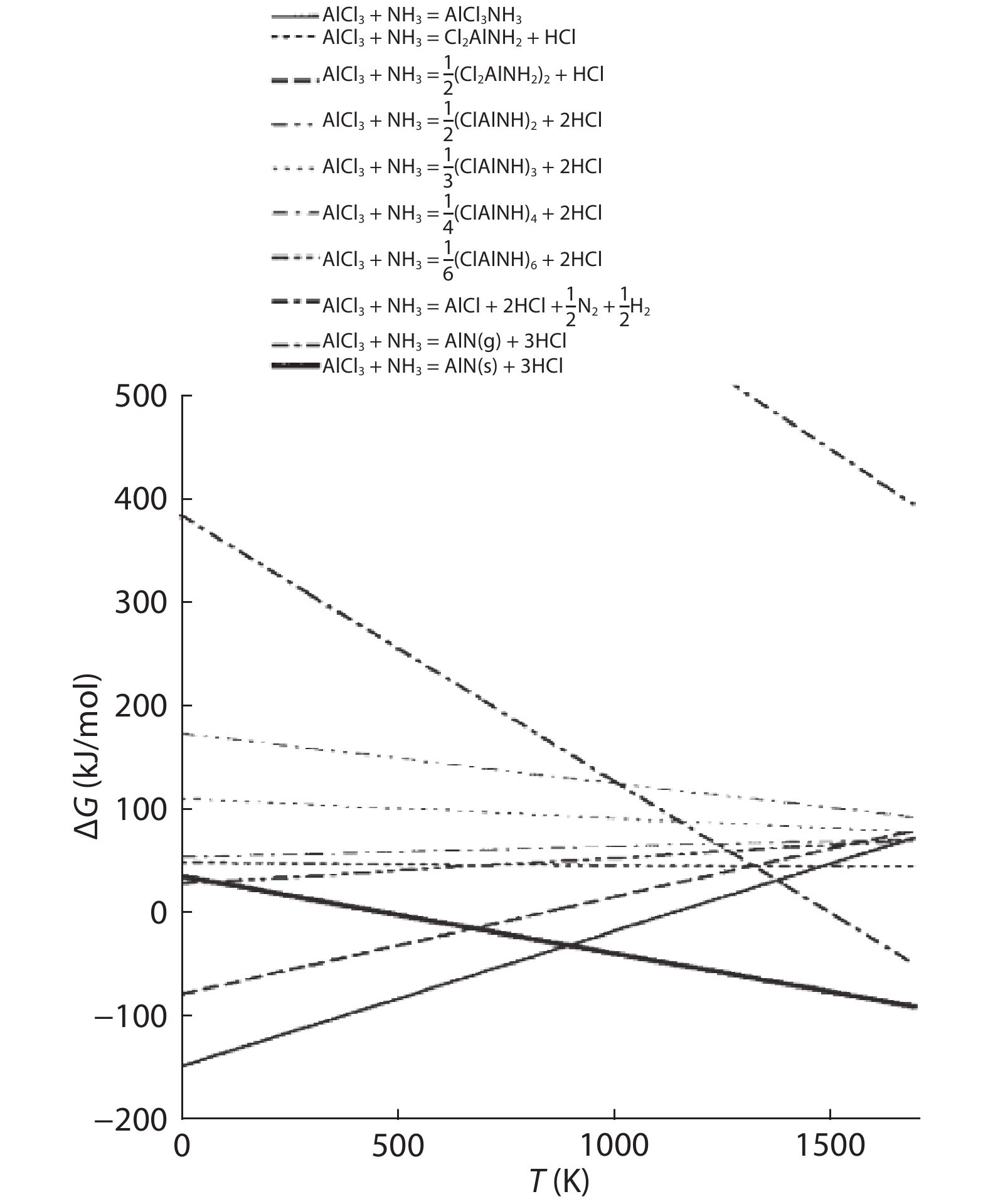
    Gibbs energy diagram for different chemical species during the growth AlN grown by CVD[34].
    Fig. 1. Gibbs energy diagram for different chemical species during the growth AlN grown by CVD[34].
    (a) The chemical reaction between the values of Ki and the change of temperature. (b) The relation between temperature and partial pressures[35].
    Fig. 2. (a) The chemical reaction between the values of Ki and the change of temperature. (b) The relation between temperature and partial pressures[35].
    The schematic diagram of low-temperature HVPE equipment[36].
    Fig. 3. The schematic diagram of low-temperature HVPE equipment[36].
    (Color online) The photo of thick AlN substrates: (a) the free-standing AlN wafer[37], (b) and (c) the 1.75-inch and 1-inch diameter AlN wafers[39], and (d) 2-inch 75 μm AlN wafer[40].
    Fig. 4. (Color online) The photo of thick AlN substrates: (a) the free-standing AlN wafer[37], (b) and (c) the 1.75-inch and 1-inch diameter AlN wafers[39], and (d) 2-inch 75 μm AlN wafer[40].
    (a) The double crystal XRC-FWHM values of (0002) and (100) planes for AlN films grown from 950 to 1100 °C[41], (b) the relationship between XRC-FWHM values of AlN (0002) rocking curves and growth rates at temperatures of 1150, 1175 and 1200 °C[42].
    Fig. 5. (a) The double crystal XRC-FWHM values of (0002) and (10 0) planes for AlN films grown from 950 to 1100 °C[41], (b) the relationship between XRC-FWHM values of AlN (0002) rocking curves and growth rates at temperatures of 1150, 1175 and 1200 °C[42].
    The SEM cross-section images of AlN films at temperatures (a) 1100, (b) 1150, (c) 1200 °C[42].
    Fig. 6. The SEM cross-section images of AlN films at temperatures (a) 1100, (b) 1150, (c) 1200 °C[42].
    (Color online) The surface morphology of AlN grown at initial stage[45].
    Fig. 7. (Color online) The surface morphology of AlN grown at initial stage[45].
    (Color online) The AFM pictures of AlN with various thickness (a) 390, (b) 650, (c) 1200 nm grown on sapphire substrates[44].
    Fig. 8. (Color online) The AFM pictures of AlN with various thickness (a) 390, (b) 650, (c) 1200 nm grown on sapphire substrates[44].
    (Color online) (a) Schematic diagram of the HT-HVPE system with high-power lamp[46]. (b) The vertical cold-wall HT-HVPE system with induce heating method[47]. (c) The conventional HVPE system with internal heating part.
    Fig. 9. (Color online) (a) Schematic diagram of the HT-HVPE system with high-power lamp[46]. (b) The vertical cold-wall HT-HVPE system with induce heating method[47]. (c) The conventional HVPE system with internal heating part.
    (Color online) Nomarski micrographs of AlN layers: (a) directly growth, (b) two-step (c) three-step[54].
    Fig. 10. (Color online) Nomarski micrographs of AlN layers: (a) directly growth, (b) two-step (c) three-step[54].
    The TEM images of the AlN films: weak beam dark field (a) g = 0002 and (b) g = 110. (c) and (d) The schematic diagram of dislocation evolution by step-growth technique[55].
    Fig. 11. The TEM images of the AlN films: weak beam dark field (a) g = 0002 and (b) g = 110. (c) and (d) The schematic diagram of dislocation evolution by step-growth technique[55].
    (Color online) (a) The XRC-FWHMs values of AlN films grown on AlN templates and sapphire substrates without nucleation layers[55]. (b) Dark-field TEM image of dislocation evolution in AlN grown on AlN/sapphire templates with g = (110)[58].
    Fig. 12. (Color online) (a) The XRC-FWHMs values of AlN films grown on AlN templates and sapphire substrates without nucleation layers[55]. (b) Dark-field TEM image of dislocation evolution in AlN grown on AlN/sapphire templates with g = (11 0)[58].
    (Color online) The AFM images of AlN grown at different temperatures: (a) 1150, (b) 1200, (c) 1400, and (d) 1450 °C[58].
    Fig. 13. (Color online) The AFM images of AlN grown at different temperatures: (a) 1150, (b) 1200, (c) 1400, and (d) 1450 °C[58].
    (Color online) The XRD θ–2 θ scans of AlN nucleation layers grown at 850 and 650 °C[61].
    Fig. 14. (Color online) The XRD θ–2 θ scans of AlN nucleation layers grown at 850 and 650 °C[61].
    The dark field TEM images for AlN epilayer grown with buffer layers, g = 110[63].
    Fig. 15. The dark field TEM images for AlN epilayer grown with buffer layers, g = 11 0[63].
    (Color online) The schematic diagram of dislocation evolution by ELOG technique[65].
    Fig. 16. (Color online) The schematic diagram of dislocation evolution by ELOG technique[65].
    (Color online) The optical microscopy pictures of AlN grown on: (a) patterned substrate and (b) flat substrate[66]. The cross-sectional SEM of AlN grown on patterned 6H-SiC with trench along (c) 00> and (d) 0> direction[67].
    Fig. 17. (Color online) The optical microscopy pictures of AlN grown on: (a) patterned substrate and (b) flat substrate[66]. The cross-sectional SEM of AlN grown on patterned 6H-SiC with trench along (c) <1 00> and (d) <11 0> direction[67].
    (Color online) (a) The section STEM images of AlN films with voids. (b) The dependence of Raman shift of E2(high) mode on the position of samples with and without voids[71]. The horizontal line is the stress-free frequency 657.4 cm–1[72].
    Fig. 18. (Color online) (a) The section STEM images of AlN films with voids. (b) The dependence of Raman shift of E2(high) mode on the position of samples with and without voids[71]. The horizontal line is the stress-free frequency 657.4 cm–1[72].
    (a) The corss-sectional SEM of voids in the interface below the 100-nm AlN buffer. (b) The photograph of self-separation AlN substrates with thickness of 79 μm[76].
    Fig. 19. (a) The corss-sectional SEM of voids in the interface below the 100-nm AlN buffer. (b) The photograph of self-separation AlN substrates with thickness of 79 μm[76].
    (Color online) The photographs: (a) the PVT-AlN substrates, (b) the free-standing AlN substrates[79].
    Fig. 20. (Color online) The photographs: (a) the PVT-AlN substrates, (b) the free-standing AlN substrates[79].
    (Color online) The optical microscopy figures of AlN thick films grown by HVPE on (a) on-axis and (b) miscut 5° PVT-AlN substrates[80].
    Fig. 21. (Color online) The optical microscopy figures of AlN thick films grown by HVPE on (a) on-axis and (b) miscut 5° PVT-AlN substrates[80].
    ParameterChemical etching technique[83]Self-separation technique[76, 77, 84]Homo-epitaxial growth technique[79, 81, 85]
    Size (cm2) 5 × 54 × 63 × 3
    Thickness (μm) 11279114
    FWHM of symmetric (arcsec)2907203431
    FWHM of skew-symmetric (arcsec)1322110432
    AdvantageSimpleLow costHigh quality
    Table 1. The freestanding AlN fabricated with different techniques.
    Maosong Sun, Jinfeng Li, Jicai Zhang, Wenhong Sun. The fabrication of AlN by hydride vapor phase epitaxy[J]. Journal of Semiconductors, 2019, 40(12): 121803
    Download Citation