
Maosong Sun, Jinfeng Li, Jicai Zhang, Wenhong Sun. The fabrication of AlN by hydride vapor phase epitaxy[J]. Journal of Semiconductors, 2019, 40(12): 121803
- Journal of Semiconductors
- Vol. 40, Issue 12, 121803 (2019)
Abstract
1. Introduction
Aluminum nitride (AlN) is one wide band gap semiconductor (up to 6.2 eV) with high-electrical resistivity (approximately 1010 Ω·cm), high coefficient of heat conductivity (3.2 W/(cm·K)), excellent acoustic wave velocity and good tolerance to chemical environments[
Though many achievements have been obtained on the research of AlN, more and more efforts should be put into the development of AlN crystal quality. In addition, it is rather difficult to obtain the high quality thick AlN wafers with crack-free and large size because of the large thermal and lattice mismatches between the foreign substrates and AlN. It was well known that the dislocation was disadvantageous to the internal quantum efficiency of deep ultraviolet devices[
Actually, AlN free-standing substrates have been obtained by PVT seeded sublimation method and the dislocation density is the lowest compared with other methods. However, the transmittance of deep ultraviolet light of AlN substrate grown by PVT was very low currently. Compared with above growth methods, hydride vapor phase epitaxy (HVPE) has many advantages, such as the simple equipment, the rapid growth rate, uniformity in large-area and low density of impurity, which make HVPE become the most perspective practical method for AlN substrates. In this paper, the recent results on the preparation of AlN by HVPE were summarized and discussed.
2. AlN growth by HVPE: Theory
HVPE is a promising method for growth of III-nitrides. It had been used to manufacture commercial 2-inch and 4-inch GaN substrates[
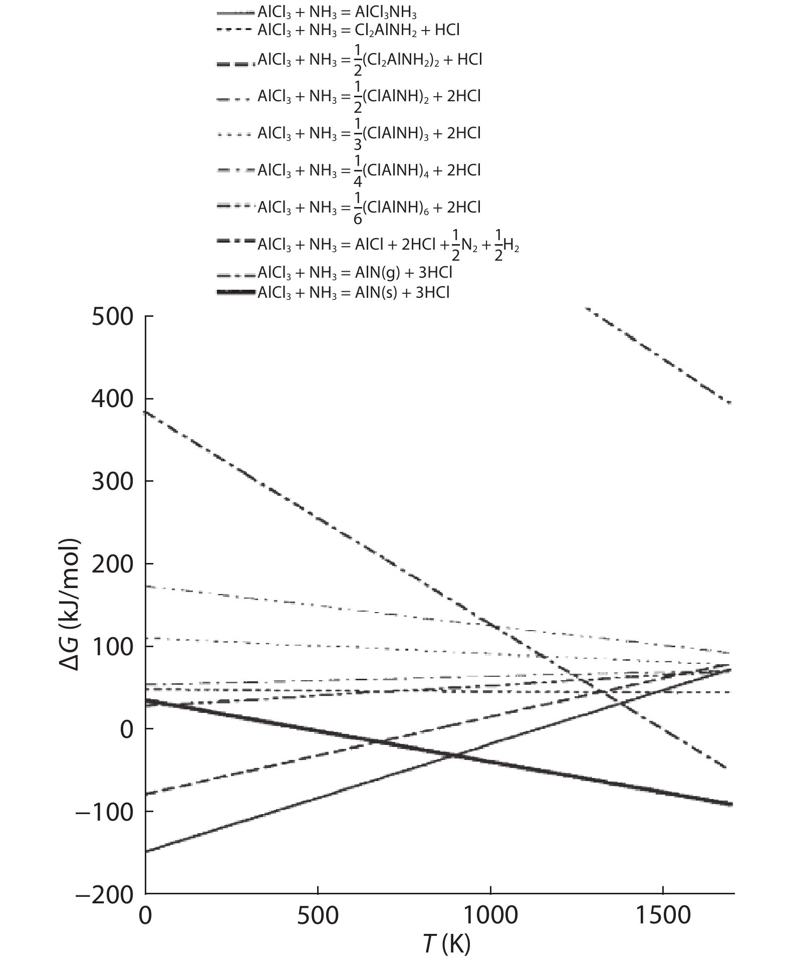
However, the chemical nature of intermediates in AlN growth is extremely complex compared to GaN growth. Fig. 1 shows the gas phase during the growth which contains a huge number of chemical species[
![]()
Figure 1.Gibbs energy diagram for different chemical species during the growth AlN grown by CVD[
Generally, the HVPE system has a quartz reactor. However, as is widely known, the quartz (SiO2) react with AlCl at high growth temperature, which will damage the quartz reactors and induce pollution for AlN growth. Fig. 2(a) shows the chemical reaction between the values of Ki and the change of temperature[
![]()
Figure 2.(a) The chemical reaction between the values of
3. AlN growth by the low-temperature HVPE: Exploration
HVPE has the advantage of high growth rate, compared with other CVD methods. In the incipient stage, most of researcher focused on the fabrication of thick AlN substrates. Fig. 3 shows the schematic diagram of low-temperature HVPE growth equipment[
![]()
Figure 3.The schematic diagram of low-temperature HVPE equipment[
There have been many reports about thick AlN substrates grown by HVPE with high growth rate. In 2000, Nikolaev et al. fabricated the AlN wafers up to 3 × 3 cm2 with thickness of 0.05 to 1 mm using HVPE technique, as shown in Fig. 4(a)[
![]()
Figure 4.(Color online) The photo of thick AlN substrates: (a) the free-standing AlN wafer[
However, few people clarified the influences of growth principles on the quality of AlN layers. In the references, the thick AlN films usually had a rough surface and poor quality. Subsequently, most of researcher focused on the effect of substrates and growing conditions. In 2002, Ledyaev et al. investigated the effect of growth temperature on the surface morphology and the crystalline quality of the AlN layers on 6H-SiC (0001) by HVPE[
Subsequently, many researchers reported the results that the crystalline quality of AlN would be improved by raising the growth temperature[
![]()
Figure 5.(a) The double crystal XRC-FWHM values of (0002) and (10
The surface morphology also improved by raising the growth temperature. Figs. 6(a)–6(c) shows the scanning electron microscope (SEM) images of AlN films grown at temperatures of 1100, 1150 and 1200 °C, respectively. The characteristics of AlN were poly-structures (Fig. 6(a)), flat structures (Fig. 6(b)) and very flat structures (Fig. 6(c)). Obviously, the higher growth temperature resulted in higher crystal quality.
![]()
Figure 6.The SEM cross-section images of AlN films at temperatures (a) 1100, (b) 1150, (c) 1200 °C[
In 2016, Zhang et al.[
![]()
Figure 7.(Color online) The surface morphology of AlN grown at initial stage[
The AFM images changed as the thickness increased. Figs. 8(a)–8(c) show the surface morphology of AlN with thickness of 390, 650 and 1200 nm, respectively. The RMS was measured to be 3.1, 3.5 and 4.2 nm for Figs. 8(a), 8(b) and 8(c), respectively. The result indicated that considerable improvement in the quality of AlN films could be produced by HVPE.
![]()
Figure 8.(Color online) The AFM pictures of AlN with various thickness (a) 390, (b) 650, (c) 1200 nm grown on sapphire substrates[
The migration of Al atoms will influence the quality and the growth rates. The lower atomic mobility, the worse quality. Moreover, the temperature of HVPE growth zone was limited to 1200 °C. In order to increase the crystalline quality and the growth rate, high temperature is required. The migration of chemical species adsorbed on growth surface can be promoted with increasing growth temperature. Then, the Al atoms are easily accommodated to the appropriate site for epitaxial growth. Therefore, the high growth temperature is essential to grow the high-quality AlN.
4. AlN growth by the high-temperature HVPE: Technology
When the temperature of hot-wall HVPE system is above 1200 °C, the quartz tube and reactors will be softened. However, the lower migration of Al adatoms n growth front induced by low growth temperature led to poor-quality of AlN films[
4.1. HT-HVPE
Generally, there were three methods to get the growth temperature above 1450 °C without softening the quartz tube. The first was using high-power lamp to heating the carbon susceptor, as shown in Fig. 9(a)[
![]()
Figure 9.(Color online) (a) Schematic diagram of the HT-HVPE system with high-power lamp[
Using of the HT-HVPE system, AlN films with high crystalline quality have been obtained. Besides, the growth rate is significantly enhanced compare to low temperature HVPE system. Based on the GaN growth techniques, for example, step-growth using buffer layers[
4.2. Step-growth technique
In 2007, Nagashima et al. reported the results of AlN grown on sapphire substrate by HT-HVPE using step-growth technique. The temperatures for the growth were above 1200 °C and the rate of growth reached 57 μm/h[
![]()
Figure 10.(Color online) Nomarski micrographs of AlN layers: (a) directly growth, (b) two-step (c) three-step[
In 2017, Su et al.[
![]()
Figure 11.The TEM images of the AlN films: weak beam dark field (a)
4.3. AlN templates with low temperature protective or nucleation layer
The initial growth stage is critical for high-quality AlN growth. In 2007, Akiyama et al. proved that c-plane sapphire could be easily decomposed at temperature over 1200 °C in H2 gas[
The nucleation layers act as a buffer layer not only protect the sapphire substrate but also reduce the lattice mismatch between sapphire substrates. It is expected to have the parameters include the appropriate thickness, the largest nucleation islands size as well as the lowest islands density[
![]()
Figure 12.(Color online) (a) The XRC-FWHMs values of AlN films grown on AlN templates and sapphire substrates without nucleation layers[
The surface morphology at different growth temperature on sapphire with nucleation layers were also studied. In 2007, Tsujisawa et al. studied the influence of the temperature on the surface morphology of AlN epilayers grown by HVPE[
![]()
Figure 13.(Color online) The AFM images of AlN grown at different temperatures: (a) 1150, (b) 1200, (c) 1400, and (d) 1450 °C[
In 2008, Tajima et al. investigated the influence of thin nucleation layers for the grown AlN layers by HVPE[
![]()
Figure 14.(Color online) The XRD
In 2017, the dislocation evolution in AlN films using different kind of buffer layers was studied by TEM[
![]()
Figure 15.The dark field TEM images for AlN epilayer grown with buffer layers,
4.4. The epitaxial lateral overgrowth (ELOG) technique
The ELOG technique was successfully used in the growth of GaN with the low dislocation density in 1997[
![]()
Figure 16.(Color online) The schematic diagram of dislocation evolution by ELOG technique[
In 2009, Okumura et al. obtained crack-free AlN by HVPE on patterned AlN/sapphire templates[
![]()
Figure 17.(Color online) The optical microscopy pictures of AlN grown on: (a) patterned substrate and (b) flat substrate[
4.5. The other technique
Recently, the patterned sapphire substrate (PSS) technique, the sputtered AlN technique, the nano-patterned sapphire substrate (NPSS) technique and other methods were reported and a series of meaningful results were obtained[
In situ formation of viods during high temperature growth were reported in 2016[
![]()
Figure 18.(Color online) (a) The section STEM images of AlN films with voids. (b) The dependence of Raman shift of
5. Free-standing AlN growth by HVPE: Expectation
All the researches aim to obtain high crystal quality and crack-free free-standing AlN substrates with lager size. During the progress several methods were proposed.
5.1. Chemical etching technique
SiC, sapphire and Si wafers are usually used as substrates AlN growth by HVPE. Sapphire and SiC are difficult to chemically etch. However, Si is easily removed by chemical etching[
5.2. Self-separation technique
The separation of the thick AlN layers from foreign substrates is critical for fabrication of freestanding substrates. The void assisted self-seperation technique was a promising method.
In order to develop the method, the chemical stability of AlN and sapphire substrate in various temperature and gas were investigated[
Following those results, 100 nm AlN/sapphire template was etched in mixed gas composed of H2, N2 and NH3 at 1450 °C. The interface beneath the thin AlN film generated a large density of voids[
![]()
Figure 19.(a) The corss-sectional SEM of voids in the interface below the 100-nm AlN buffer. (b) The photograph of self-separation AlN substrates with thickness of 79
5.3. Homo-epitaxial growth technique
The homo-epitaxial growth technique was applied to fabricate free-standing AlN on PVT-AlN substrates[
![]()
Figure 20.(Color online) The photographs: (a) the PVT-AlN substrates, (b) the free-standing AlN substrates[
Nomura et al. investigated the influence of miscut angles of AlN substrates prepared by sublimation method on the surface morphology b of AlN grown by HVPE. The miscut angle was inclined toward the <11
![]()
Figure 21.(Color online) The optical microscopy figures of AlN thick films grown by HVPE on (a) on-axis and (b) miscut 5° PVT-AlN substrates[
At last, the difference growth techniques of free-standing AlN have been summarized. The advantages and the best results are shown in Table 1. The self-separation technique may be the most promising growth technology in the near future.
6. Prospect
In recent years, with the rapid increase of the market for high-quality AlN substrate with low-cost and large size, various techniques and modification have been made in HVPE growth system and processes. At present, the HVPE system still plays an important role in the fabrication of thick AlN layers with high ultraviolet transmittance, which is very important for AlN-based deep ultraviolet optoelectronics. However, the threading dislocations and the residual stress primarily limited its application.
The difference of lattice constants and thermal expansion coefficients will result in the crack and strain in the AlN wafers, which is an issue need to be solved. Another issue is the threading dislocations. Nowadays, the high quality AlN with large size grown by HVPE are still under research. We believe that with the efforts of researchers, 2-inch AlN freestanding substrate with high crystal-quality and high ultraviolet transmittance will be realized in 3 years. Due to the lack of native substrate, the dislocation density of AlN grown by HVPE will be around 106 cm–2 and it is difficult to decrease furthermore. In addition, the cost for freestanding AlN substrate produced by HVPE will be higher than that grown by PVT due to the limitation of growth rate of HVPE. However, we noticed that AlN grown by PVT will absorb the deep ultraviolet light seriously. Until now, HVPE is still one promising method to produce the ultraviolet transparent AlN freestanding substrate.
Acknowledgments
This work was partly supported by Beijing Municipal Natural Science Foundation (No. 4182046), the National Natural Science Foundation of China (No. 61874007), the Fundamental Research Funds for the Central Universities (Nos. buctrc201802, buctrc201830), the Funding for Bagui Talent of Guangxi province (Nos. T31200992001 and T3120097921), ASEAN Young Talented Scientist Program (No. Y312001913) and Talent Model Base, China (No. AE31200065).
References
[1] V Avrutin, D J Silversmith, Y Mori et al. Growth of bulk GaN and AlN: progress and challenges. Proc IEEE, 98, 1302(2010).
[2] T Paskova, D A Hanser, K R Evans. GaN substrates for III-nitride devices. Proc IEEE, 98, 1324(2010).
[3] U K Mishra, P Parikh, Y F Wu. AlGaN/GaN HEMTs — An overview of device operation and applications. Proc IEEE, 90, 1022(2002).
[4] V Adivarahan, W H Sun, A Chitnis et al. 250 nm AlGaN light-emitting diodes. Appl Phys Lett, 85, 2175(2004).
[5] H Hirayama, T Yatabe, N Noguchi et al. 231–261 nm AlGaN deep-ultraviolet light-emitting diodes fabricated on AlN multilayer buffers grown by ammonia pulse-flow method on sapphire. Appl Phys Lett, 91, 071901(2007).
[6] R Jain, W Sun, J Yang et al. Migration enhanced lateral epitaxial overgrowth of AlN and AlGaN for high reliability deep ultraviolet light emitting diodes. Appl Phys Lett, 93, 051113(2008).
[7] J C Zhang, Y H Zhu, T Egawa et al. Suppression of the subband parasitic peak by 1 nm i-AlN interlayer in AlGaN deep ultraviolet light-emitting diodes. Appl Phys Lett, 93, 131117(2008).
[8] H Hirayama, S Fujikawa, N Noguchi et al. 222–282 nm AlGaN and InAlGaN-based deep-UV LEDs fabricated on high-quality AlN on sapphire. Phys Status Solidi A, 206, 1176(2009).
[9] N Susilo, S Hagedorn, D D et al. AlGaN-based deep UV LEDs grown on sputtered and high temperature annealed AlN/sapphire. Appl Phys Lett, 112, 041110(2018).
[10] V Adivarahan, S Wu, W H Sun et al. High-power deep ultraviolet light-emitting diodes based on a micro-pixel design. Appl Phys Lett, 85, 1838(2004).
[11] W H Sun, J P Zhang, V Adivarahan et al. AlGaN-based 280 nm light-emitting diodes with continuous wave powers in excess of 1.5 mW. Appl Phys Lett, 85, 531(2004).
[12] J C Zhang, Y H Zhu, T Egawa et al. Quantum-well and localized state emissions in AlInGaN deep ultraviolet light-emitting diodes. Appl Phys Lett, 91, 221906(2007).
[13] J C Zhang, Y Sakai, T Egawa. Low-temperature electroluminescence quenching of AlGaN deep ultraviolet light-emitting diodes. Appl Phys Lett, 96, 013503(2010).
[14] M Shatalov, W H Sun, A Lunev et al. AlGaN deep-ultraviolet light-emitting diodes with external quantum efficiency above 10%. Appl Phys Express, 5, 082101(2012).
[15] S X Tan, J C Zhang, T Egawa et al. Influence of quantum-well width on the electroluminescence properties of AlGaN deep ultraviolet light-emitting diodes at different temperatures. Nanoscale Res Lett, 13, 334(2018).
[16] M Kneissl, T Kolbe, C Chua et al. Advances in group III-nitride-based deep UV light-emitting diode technology. Semicond Sci Tech, 26, 014036(2011).
[17] M Yano, M Okamoto, Y K Yap et al. Growth of nitride crystals, BN, AlN and GaN by using a Na flux. Diam Relat Mater, 9, 512(2000).
[18] Y Kangawa, R Toki, T Yayama et al. Novel solution growth method of bulk AlN using Al and Li3N solid sources. Appl Phys Express, 4, 095501(2011).
[19] B G Wang, M J Callahan. Ammonothermal synthesis of III-nitride crystals. Cryst Growth Des, 6, 1227(2006).
[20] G A Slack, T F Mcnelly. Growth of high-purity AlN crystals. J Cryst Growth, 34, 263(1976).
[21] Z G Herro, D Zhuang, R Schlesser et al. Growth of AlN single crystalline boules. J Cryst Growth, 312, 2519(2010).
[22] R T Bondokov, S G Mueller, K E Morgan et al. Large-area AlN substrates for electronic applications: An industrial perspective. J Cryst Growth, 310, 4020(2008).
[23] Y N Makarov, O V Avdeev, I S Barash et al. Experimental and theoretical analysis of sublimation growth of AlN bulk crystals. J Cryst Growth, 310, 881(2008).
[24] C Hartmann, A Dittmar, J Wollweber et al. Bulk AlN growth by physical vapour transport. Semicond Sci Tech, 29, 084002(2014).
[25] J Bai, M Dudley, W H Sun et al. Reduction of threading dislocation densities in AlN/sapphire epilayers driven by growth mode modification. Appl Phys Lett, 88, 051903(2006).
[26] M Imura, N Fujimoto, N Okada et al. Annihilation mechanism of threading dislocations in AlN grown by growth form modification, method using V/III ratio. J Cryst Growth, 300, 136(2007).
[27] R G Banal, M Funato, Y Kawakamia. Initial nucleation of AlN grown directly on sapphire substrates by metal-organic vapor phase epitaxy. Appl Phys Lett, 92, 241905(2008).
[28] M Takeuchi, S Ooishi, T Ohtsuka et al. Improvement of AI-polar AIN layer quality by three-stage flow-modulation metalorganic chemical vapor deposition. Appl Phys Express, 1, 021102(2008).
[29] L S Zhang, F J Xu, J M Wang et al. High-quality AlN epitaxy on nano-patterned sapphire substrates prepared by nano-imprint lithography. Sci Rep-Uk, 6, 35934(2016).
[30] D Lee, J W Lee, J Jang et al. Improved performance of AlGaN-based deep ultraviolet light-emitting diodes with nano-patterned AlN/sapphire substrates. Appl Phys Lett, 110, 191103(2017).
[31] H L Long, J N Dai, Y Zhang et al. High quality 10.6
[32] J A Freitas, G C B Braga, W J Moore et al. Structural and optical properties of thick freestanding GaN templates. J Cryst Growth, 231, 322(2001).
[33] L Liu, J H Edgar. Substrates for gallium nitride epitaxy. Mat Sci Eng R, 37, 61(2002).
[34] A Y Timoshkin, H F Bettinger, H F Schaefer. The chemical vapor deposition of aluminum nitride: Unusual cluster formation in the gas phase. J Am Chem Soc, 119, 5668(1997).
[35] Y Kumagai, T Yamane, T Miyaji et al. Hydride vapor phase epitaxy of AlN: thermodynamic analysis of aluminum source and its application to growth. Phys Status Solidi C, 0, 2498(2003).
[36] O Y Ledyaev, A E Cherenkov, A E Nikolaev et al. Properties of AlN layers grown on SiC substrates in wide temperature range by HVPE. International Workshop on Nitride Semiconductors, Proceedings, 474(2002).
[37] A Nikolaev, I Nikitina, A Zubrilov et al. AlN wafers fabricated by hydride vapor phase epitaxy. MRS Internet J N S R, 5, W6.5(2000).
[38] Y Melnik, D Tsvetkov, A Pechnikov et al. Characterization of AlN/SiC epitaxial wafers fabricated by hydride vapour phase epitaxy. Phys Status Solidi A, 188, 463(2001).
[39] Y Melnik, V Soukhoveev, V Ivantsov et al. AlN substrates: fabrication via vapor phase growth and characterization. Phys Status Solidi A, 200, 22(2003).
[40] O Kovalenkov, V Soukhoveev, V Ivantsov et al. Thick AlN layers grown by HVPE. J Cryst Growth, 281, 87(2005).
[41] Y Kumagai, T Yamane, A Koukitu. Growth of thick AlN layers by hydride vapor-phase epitaxy. J Cryst Growth, 281, 62(2005).
[42] Y H Liu, T Tanabe, H Miyake et al. Fabrication of thick AlN film by low pressure hydride vapor phase epitaxy. Phys Status Solidi C, 3, 1479(2006).
[43] Y H Liu, T Tanabe, H Miyake et al. Growth of thick AlN layer by hydride vapor phase epitaxy. Jpn J Appl Phys Part 2, 44, 505(2005).
[44] M S Sun, J C Zhang, J Huang et al. AlN thin film grown on different substrates by hydride vapor phase epitaxy. J Cryst Growth, 436, 62(2016).
[45] X J Gong, K Xu, J Huang et al. Evolution of the surface morphology of AlN epitaxial film by HVPE. J Cryst Growth, 409, 100(2015).
[46] K I Eriguchi, H Murakami, U Panyukova et al. MOVPE-like HVPE of AlN using solid aluminum trichloride source. J Cryst Growth, 298, 332(2007).
[47] N Coudurier, R Boichot, V Fellmann et al. Effects of the V/III ratio on the quality of aluminum nitride grown on (0001) sapphire by high temperature hydride vapor phase epitaxy. Phys Status Solidi C, 10, 362(2013).
[48] A Claudel, V Fellmanna, I Gelard et al. Influence of the V/III ratio in the gas phase on thin epitaxial AlN layers grown on (0001) sapphire by high temperature hydride vapor phase epitaxy. Thin Solid Films, 573, 140(2014).
[49] T Nagashima, M Harada, H Yanagi et al. High-speed epitaxial growth of AlN above 1200 °C by hydride vapor phase epitaxy. J Cryst Growth, 300, 42(2007).
[50] H Amano, N Sawaki, I Akasaki et al. Metalorganic vapor-phase epitaxial-growth of a high-quality gan film using an AlN buffer layer. Appl Phys Lett, 48, 353(1986).
[51] A Usui, H Sunakawa, A Sakai et al. Thick GaN epitaxial growth with low dislocation density by hydride vapor phase epitaxy. Jpn J Appl Phys Part 2, 36, L899(1997).
[52] O Ambacher. Growth and applications of Group III nitrides. J Phys D, 31, 2653(1998).
[53] X H Wu, D Kapolnek, E J Tarsa et al. Nucleation layer evolution in metal-organic chemical vapor deposition grown GaN. Appl Phys Lett, 68, 1371(1996).
[54] T Nagashima, M H Ma, H Yanagi et al. Improvement of AlN crystalline quality with high epitaxial growth rates by hydride vapor phase epitaxy. J Cryst Growth, 305, 355(2007).
[55] X J Su, J C Zhang, J Huang et al. Defect structure of high temperature hydride vapor phase epitaxy-grown epitaxial (0001) AlN/sapphire using growth mode modification process. J Cryst Growth, 467, 82(2017).
[56] K Akiyama, T Araki, H Murakami et al. In situ gravimetric monitoring of decomposition rate on the surface of (0001)
[57] D G Zhao, J J Zhu, Z S Liu et al. Surface morphology of AlN buffer layer and its effect on GaN growth by metalorganic chemical vapor deposition. Appl Phys Lett, 85, 1499(2004).
[58] K Tsujisawa, S Kishino, Y H Liu et al. High temperature growth of AlN film by LP-HVPE. Phys Status Solidi C, 4, 2252(2007).
[59] J Tajima, H Murakami, Y Kumagai et al. Preparation of a crack-free AlN template layer on sapphire substrate by hydride vapor-phase epitaxy at 1450 °C. J Cryst Growth, 311, 2837(2009).
[60] J Tajima, Y Kubota, R Togashi et al. Growth of thin protective AlN layers on sapphire substrates at 1065 °C for hydride vapor phase epitaxy of AlN above 1300 °C. Phys Status Solidi C, 5, 1515(2008).
[61] M Balaji, A Claudel, V Fellmann et al. Effects of AlN nucleation layers on the growth of AlN films using high temperature hydride vapor phase epitaxy. J Alloy Compd, 526, 103(2012).
[62] H Miyake, G Nishio, S Suzuki et al. Annealing of an AlN buffer layer in N2–CO for growth of a high-quality AlN film on sapphire. Appl Phys Express, 9, 025501(2016).
[63] J Huang, M T Niu, J C Zhang et al. Reduction of threading dislocation density for AlN epilayer via a highly compressive-stressed buffer layer. J Cryst Growth, 459, 159(2017).
[64] X J Su, J Huang, J P Zhang et al. Microstructure and influence of buffer layer on threading dislocations in (0001) AlN/sapphire grown by hydride vapor phase epitaxy. J Cryst Growth, 515, 72(2019).
[65] M Imura, K Nakano, G Narita et al. Epitaxial lateral overgrowth of AlN on trench-patterned AlN layers. J Cryst Growth, 298, 257(2007).
[66] Y Katagiri, S Kishino, K Okuura et al. Low-pressure HVPE growth of crack-free thick AlN on a trench-patterned AlN template. J Cryst Growth, 311, 2831(2009).
[67] K Okumura, T Nomura, H Miyake et al. HVPE growth of AlN on trench-patterned 6H-SiC substrates. Phys Status Solidi C, 8, 467(2011).
[68] G S Lee, C Lee, H Jeon et al. Growth of AlN layer on patterned sapphire substrate by hydride vapor phase epitaxy. Jpn J Appl Phys, 55, 05FC02(2016).
[69] S Y Xiao, R Suzuki, H Miyake et al. Improvement mechanism of sputtered AlN films by high-temperature annealing. J Cryst Growth, 502, 41(2018).
[70] S Xiao, N Jiang, K Shojiki et al. Preparation of high-quality thick AlN layer on nanopatterned sapphire substrates with sputter-deposited annealed AlN film by hydride vapor-phase epitaxy. Jpn J Appl Phys, 58, SC1003(2019).
[71] X H Liu, J C Zhang, X J Su et al. Fabrication of crack-free AlN film on sapphire by hydride vapor phase epitaxy using an in situ etching method. Appl Phys Express, 9(2016).
[72] T Prokofyeva, M Seon, J Vanbuskirk et al. Vibrational properties of AlN grown on (111)-oriented silicon. Phys Rev B, 63, 125313(2001).
[73] Z P Huang, N Geyer, P Werner et al. Metal-assisted chemical etching of silicon: a review. Adv Mater, 23, 285(2011).
[74] K Akiyama, H Murakami, Y Kumaga et al. In situ gravimetric monitoring of decomposition rate on surface of (10(1)over-bar2) r-plane sapphire for high-temperature growth of nonpolar AlN. Jpn J Appl Phys, 47, 3434(2008).
[75] Y Kumagai, K Akiyama, R Togashi et al. Polarity dependence of AlN {0001} decomposition in flowing H2. J Cryst Growth, 305, 366(2007).
[76] Y Kumagai, Y Enatsu, M Ishizuki et al. Investigation of void formation beneath thin AlN layers by decomposition of sapphire substrates for self-separation of thick AlN layers grown by HVPE. J Cryst Growth, 312, 2530(2010).
[77] Y Kumagai, J Tajima, M Ishizuki et al. Self-separation of a thick AIN layer from a sapphire substrate via interfacial voids formed by the decomposition of sapphire. Appl Phys Express, 1, 045003(2008).
[78] M S Sun, J C Zhang, J Huang et al. Influence of thickness on strain state and surface morphology of AlN grown by HVPE. J Semicond, 37, 045501(2016).
[79] Y Kumagai, Y Kubota, T Nagashima et al. Preparation of a freestanding AIN substrate from a thick AIN layer grown by hydride vapor phase epitaxy on a bulk AIN substrate prepared by physical vapor transport. Appl Phys Express, 5, 055504(2012).
[80] T Nomura, K Okumura, H Miyake et al. AIN homoepitaxial growth on sublimation-AIN substrate by low-pressure HVPE. J Cryst Growth, 350, 69(2012).
[81] T Nagashima, A Hakomori, T Shimoda et al. Preparation of freestanding AlN substrates by hydride vapor phase epitaxy using hybrid seed substrates. J Cryst Growth, 350, 75(2012).
[82] Y Watanabe, H Miyake, K Hiramatsu et al. HVPE homoepitaxy on freestanding AlN substrate with trench pattern. Phys Status Solidi C, 12, 334(2015).
[83] Y Kumagai, T Nagashima, A Koukitu. Preparation of a freestanding AlN substrate by hydride vapor phase epitaxy at 1230 °C using (111) Si as a starting substrate. Jpn J Appl Phys Part 2, 46, L389(2007).
[84] J A Freitas, J C Culbertson, M A Mastro et al. Structural and optical properties of thick freestanding AlN films prepared by hydride vapor phase epitaxy. J Cryst Growth, 350, 33(2012).
[85] V Soukhoveev, A Volkova, V Ivantsov et al. Large area GaN and AlN template substrates fabricated by HVPE. Phys Status Solidi C, 6, S333(2009).

Set citation alerts for the article
Please enter your email address
© Copyright 2018-2021 | Chinese Laser Press. All Rights Reserved 沪ICP备15018463号-20