• Journal of Semiconductors
  • Vol. 43, Issue 4, 042501 (2022)
Wenrong Liu, Xinyang Li, Changwen Zhang, and Shishen Yan
Author Affiliations
  • School of Physics and Technology, Spintronics Institute, University of Jinan, Jinan 250022, China
  • show less
    DOI: 10.1088/1674-4926/43/4/042501 Cite this Article
    Wenrong Liu, Xinyang Li, Changwen Zhang, Shishen Yan. Janus VXY monolayers with tunable large Berry curvature[J]. Journal of Semiconductors, 2022, 43(4): 042501 Copy Citation Text show less

    Abstract

    The Rashba effect and valley polarization provide a novel paradigm in quantum information technology. However, practical materials are scarce. Here, we found a new class of Janus monolayers VXY (X = Cl, Br, I; Y = Se, Te) with excellent valley polarization effect. In particular, Janus VBrSe shows Zeeman type spin splitting of 14 meV, large Berry curvature of 182.73 bohr2, and, at the same time, a large Rashba parameter of 176.89 meV·Å. We use the k·p theory to analyze the relationship between the lattice constant and the curvature of the Berry. The Berry curvature can be adjusted by changing the lattice parameter, which will greatly improve the transverse velocities of carriers and promote the efficiency of the valley Hall device. By applying biaxial strain onto VBrSe, we can see that there is a correlation between Berry curvature and lattice constant, which further validates the above theory. All these results provide tantalizing opportunities for efficient spintronics and valleytronics.

    1. Introduction

    Two-dimensional (2D) materials[16] have become the main topic of discussion because of their ample physical properties, after graphene[7] was successfully synthesized and became a research hotspot. In recent years, a new type of intrinsic degree of freedom "energy valley" of electrons has been discovered and used to research and develop new electronic devices[8]. Similar to the electron spin degree of freedom, the energy valley degree of freedom is also called pseudospin[911]. Compared with traditional devices, energy valley devices have the advantages of fast calculation speed, high integration, less information distortion, and low energy consumption[1214]. Therefore, "valley electronics" has been the focus of condensed matter in recent years.

    The development of valley electronics is inseparable from the research of 2D atomic layer materials, especially, 2D transition metal dichalcogenides (TMDCs) have attracted widespread attention as potential low-dimensional grain materials[15]. Their spatial reversal symmetry is destroyed, with two degenerates but not equivalent valley states produced at the K point and K’ point of the Brillouin zone which is hexagonal[1618], which are called K valley materials. TMDCs materials have become an important research platform for studying energy valley effects and building energy valley devices. In addition to graphene and TMDCs, some 2D materials had been calculated to exist valley-contrasting properties, such as MnPSe3[10], Tl2O[19], and Tl/SiC[20], MoSi2N4[21], TiSiCO[22].

    Monolayer semiconductor MX2 is composed of two layers of chalcogen atoms and a layer of transition metal atoms stacked with ABA, so it only shows the mirror reflection symmetry of spin splitting caused by spin-orbit coupling (SOC) in the out-of-plane direction[23]. Li et al. use a unique synthesis method, substituting Se atoms for the top layer S, to get the Janus monolayer of MoSSe[24, 25]. For one thing, Janus MoSSe maintains the characteristics of the valley and has great promise of becoming a useful 2D valley electronic material[26]. For another, owing to its inherent vertical dipole, Janus MoSSe exhibits Rashba-type spin splitting near the point Γ[27]. What fits our idea is that MXY retains the outstanding functions of MX2, thereby expanding the application of TMDCs. It is inferred that MXY can be used as a water splitting photocatalyst with high efficiency[28, 29] and piezoelectric due to the inherent out-of-plane dipole, a 2D material in device applications[30]. In 2020, Zhang et al.[31] investigated the electronic structure and magnetic properties of Janus Cr2I3X3 (X = Br, Cl) monolayers by DFT calculations. They found that there was a strain-induced transition from half semiconductor to bipolar magnetic semiconductor and a reversal of magnetic axis. Subsequently, Li et al.[32] systematically studied the magnetic properties of Janus FeXY (X, Y = Cl, Br, and I, X ≠ Y) monolayers, which are half-metals with large gaps in spin-up channels. Based on the Goodenough–Kanamori–Anderson theory, the ferromagnetism stems from the super-exchange interaction mediated by Fe–X/Y–Fe bonds. They also found that FeClBr monolayer shows ferromagnetic character with spontaneous valley polarization due to the interaction of magnetic exchange interaction and spin-orbit coupling effect, and the anomalous valley Hall effect can be realized under an in-plane electrical field[33]. These results enrich the diversity of Janus 2D materials, which have potential applications in 2D spintronic devices.

    In addition, some treatments have been performed on the spin splitting and valley-bottom polarization in MXY materials, such as electric field[34], strain[24] and magnetically doped[35]. Plane the asymmetry of the outer mirror lets Janus MoSSe which has C3v symmetry become a monolayer of polarity and causes the accompanying Rashba-type and Zeeman-type spin splitting, which undoubtedly has broad prospects in novel physical phenomena and practical applications, such as information transfer with multiple transmission ways. So far, two-dimensional monolayers, which have Rashba-type spin splitting and spin-valley coupling, are little described as before, simultaneously, they are limited to Janus TMDCs with 2H phase, such as MoSSe.

    Considering that the 2H-VSe2 monolayer has been prepared experimentally[36], this provides the basis for the subsequent synthesis of Janus monolayers. As many studies have reported, ordered Janus MXY is synthesized under careful control through optimized chemical vapor deposition (CVD) method to avoid the formation of random alloys[24, 25, 37, 38]. On account of synthesizing of Janus MoSSe by CVD methods[25, 38], consequently, experimental implementation of Janus VXY could be anticipated by making use of a strategy alike to Janus MoSSe. Janus VXY has C3v symmetry, and the asymmetry of the plane mirror lets it a monolayer of polarity, which will lead to the accompanying Zeeman type and Rashba type spin splitting. And because of its large atomic number, there will be a stronger SOC effect, resulting in larger Rashba splitting. Here we propose a new 2H Janus monolayer, VXY (X = Cl, Br, I; Y = Se, Te), which has a larger Berry curvature and a larger Rashba parameter. The Janus VXY in the 2H phase with C3v symmetry shows a middling band gap and has electronic properties similar to Janus TMDC. As a polar monolayer, Janus VXY is considered to be dynamic and thermal stability. Compared with Janus MoSSe (64.64 bohr2), Janus VXY has a larger Berry curvature. In particular, the Berry curvature of Janus VITe (335.76 bohr2) is practically quintuple that of Janus MoSSe. Moreover, Janus VBrSe (176.89 meV·Å) has a larger Rashba-type spin splitting than WSSe (158 meV·Å)[28] and MoSSe (77 meV·Å)[25]. More particularly, we propose that biaxial strain can regulate the Berry curvature which is based on a theory called k·p perturbation[39, 40]. By applying biaxial strains on Janus VBrSe to adjust its lattice constant, this conclusion can be further verified. It was recognized as a viable strategy[41]. This work hews out a novel way to realize efficient valley electronic and spin electron logic devices.

    2. Computational methods

    We calculate all structures and their electronic properties based on the Vienna ab initio simulation software package of spin-polarized density functional theory (DFT)[42]. The exchange correlation potential is characterized by the Perdew–Burke–Ernzerhof (PBE)[43] of the generalized gradient approximation (GGA)[44]. The ion–electron potential is described by the projected argument wave (PAW)[45]. Certainly, we also optimize the structure by using Hubbard U (2.7 eV) and spin dependent GGA, which is to approximately describe correlated interaction of metal V elements[46]. The energy cutoff of the plane wave is 500 eV. The Brillouin zone uses a convergent 11 × 11 × 1 k mesh for structural relaxation and 15 × 15 × 1 k mesh for electronic analysis. Both the atomic position and the lattice constant are relaxed until the energy and force converge to 10–7 eV/atom and 0.001 eV/Å. For Janus VXY, a vacuum space of about 20 Å is applied along the c direction in order to avoid the interaction among adjacent layers. Based on the density of functional perturbation theory[47], the phonon dispersion spectrum of Janus VXY was calculated with the PHONOPY program[48], and in this process, we use a 4 × 4 × 1 supercell. Under the conditions of 300 K and 10 ps time step, a 3 × 3 × 1 supercell is simulated by Ab initio molecular dynamics (AIMD)[49]. The Berry curvature of Janus VXY is calculated by the maximum local Wannier functions implemented in the WANNIER90 package[50].

    3. Results and discussion

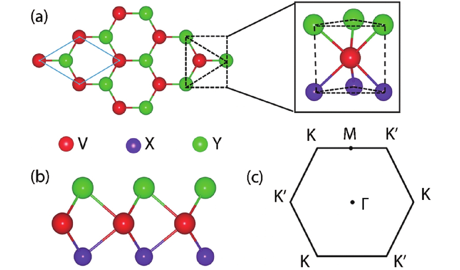
    2H-phases of Janus VXY (X = Cl, Br, I; Y = Se, Te) monolayer consists of a VX2 monolayer in which X atoms are replaced by Y atoms. By the views from top and side in Figs. 1(a) and 1(b), it still presents a hexagonal lattice. Hence, the 2H-phase Janus VXY are taken into account in this study. V atoms form a triangular prism, and six halide atoms are vertices of the triangular prism, which is similar to the TMDCs of 2H phase. The point groups of VX2 and VXY monolayers are D3d and C3v, respectively. In reciprocal space, the high-symmetry points are Γ (0,0,0), K (–1/3,2/3,0), M (–0.5,0.5,0) and K' (–2/3,1/3,0). The bond length of V–X is different from that of V–Y, the distance between the three atomic layers and lattice constants of monolayer VXY are shown in Table 1. We also find that VXY monolayers are non-magnetic, which is different from the findings of Smaili et al.[51]. They computed the magnetic properties of Janus VSeTe monolayer and found ferromagnetic order for all elements. As shown in Table 1, the local magnetic moments of V atoms are 0.000 µB. And we predict that the three d orbital electrons of V atoms give two to Se atoms and one to Cl atom respectively. In addition, formation energy Ec of VXY is also in Table 1.

    (Color online) (a, b) Top and side views of SL VXY. The illustrations in (a) indicate VXY trigonal prismatic geometry. (c) The 2D Brillouin zone of VXY.

    Figure 1.(Color online) (a, b) Top and side views of SL VXY. The illustrations in (a) indicate VXY trigonal prismatic geometry. (c) The 2D Brillouin zone of VXY.

    Table Infomation Is Not Enable

    As shown in Fig. S1, the phonon dispersion relationship between Janus VXY and the remainder TMH structures of 2H phase indicates that phonon branches throughout Brillouin region are all positive, demonstrating dynamic stability. We also utilize AIMD simulations, which can be found in Fig. S2. The outcomes show that there is no significant structural failure occurs after 10 ps at 300 K, which indicates the thermodynamic stability of structures. In addition, we also calculate elastic constants of SL VXY. As a reference, the elastic constants of C11, C21, C12, C22 and C66 satisfy the Born criteria (C11C22C12C21 > 0 and C 66 > 0), indicating that SL VXY ensures mechanical stability. In order to summarize the bonding characteristics in SL VXY, we calculate its electron localization function (ELF). The ELF indicates the existence of two localized areas: one around V atoms and others around Se and Br atoms, as shown in Fig. S4 in the Supporting Information. There are almost no electrons between V and Br/Se atoms, which shows that there is a typical ionic bond, and V atoms provide electrons to Br/Se atoms.

    Then we center upon the electronic properties of VXY monolayer. After analyzing the energy band of VXY in Fig. S3, one can see that Janus VXY shows similar electronic properties. Therefore, we will introduce the results of Janus VBrSe in the following sections. In Fig. 2, energy band structures of Janus VBrSe without and with SOC are shown. Both the valence band maximum (VBM) and the conduction band minimum (CBM) are located at point K/K'. As shown in Fig. 2(b), without considering SOC, the contribution of energy bands which are near the Fermi level comes entirely from the V-3 d orbitals, one of which is completely occupied. When SOC was considered (see Fig. 2(b)), the band splitting at the high symmetry point happens when the orbit distribution remains unchanged. Obviously, the electronic band structure of Janus VXY is similar with that of MoSSe and WSSe monolayers (Eg ~ 1.5 eV) [52]. In other words, the highest valence band is totally separated from the lower valence band with a limited energy gap.

    (Color online) (a) Calculated electronic band structures of the VBrSe monolayer without and with SOC. (b) The projected band structures of the VbrSe monolayer without and with SOC, respectively.

    Figure 2.(Color online) (a) Calculated electronic band structures of the VBrSe monolayer without and with SOC. (b) The projected band structures of the VbrSe monolayer without and with SOC, respectively.

    Furthermore, it should be clearly explained that owing to the different Hamiltonian between them, the SOC splitting which is at point Γ is regarded as Rashba type, not Dresselhaus type. When the spin splitting belongs to Rashba-type, the Hamiltonian can be showed as , as well as the Dresselhaus-type spin splitting can be calculated by , in which k and σ mean the in-plane momentum and Pauli matrices, respectively. An important feature of VXY monolayer is the beingness of Rashba spin splitting, which is different from the mirror symmetrical TMDCs. The Rashba SOC effect has two significant characteristics: spin splitting and energy band splitting[53]. Here, the magnitude of SOC-induced spin splitting is characterized by the energy band splitting ( ) of the splitting state and the Rashba parameter ( ), which can measure the strength of the spin splitting[54]. The spin texture around Γ and band structure splitting are shown in Figs. 3(a) and 3(b).

    (Color online) (a, b) In-plane spin-polarization components of two bands around Γ. (c) Magnified view of the band structure around Γ. (d) Spin texture of Janus VBrSe.

    Figure 3.(Color online) (a, b) In-plane spin-polarization components of two bands around Γ. (c) Magnified view of the band structure around Γ. (d) Spin texture of Janus VBrSe.

    The spins of the two highest valence bands are not only opposite, but also conform to the following relationship: . The Rashba parameter is made an approximation by the formula , where and are the wave vector and splitting of the energy, respectively. They are also marked in Fig. 3(c). The splitting energy and Rashba parameter of WSSe monolayer are 3.64 and 166 meV·Å, respectively[55]. The Rashba parameters of other VXY structures can be found in Table 2. It can be seen that the energy splitting values of VXY are a bit larger compared to that of WSSe[55]. If the carrier passes through the semiconductor, the effective magnetic field of SOC will abruptly change due to the scattering of the momentum change, resulting in spin randomization. Generally, a larger Rashba parameter indicates a larger SOC interaction, which is ideal to suppress spin relaxation, control spin precession, and have robustness to all modalities of spin-independent scattering. Considering the practical application, we prefer to have a larger Rashba-type split structure. For Janus VBrSe, the calculated is 176.89 meV·Å. We find that it is larger than Janus MoSSe (77 meV Å)[35], and can be compared with MoSTe (147 meV·Å)[56] and WSSe (166 meV·Å)[55] is comparable, as shown in Fig. 4. The Rashba parameters of Janus VBrSe is larger, and the Rashba type spin splitting is determined by energy band structure, Rashba coefficient and spin texture. The Rashba parameter, which is larger, proves that VBrSe can be considered as a material of great significance for the development of spin field effect transistors. We also find that the effect of different k-points or energy cutoff on band structures is not significant, as shown in Figs. S5 and S6 in the Supporting Information. The analysis of the energy bands in Table SI have showed that different k-points and energy cutoff have no effect on wave vector ( ). Janus VBrSe still has a large Rashba constant, ensuring that it is important for spin field effect transistor development. Meanwhile, as shown in Fig. S7, the calculated results at several Hubbard U values illustrate that they have similar energy band structures. We also analysis the corresponding energy band in Table S2, showing that different U values affect the energy splitting of VBrSe as well as the wave vector, leading to differences in the Rashba constants.

    Table Infomation Is Not Enable

    (Color online) Comparison of Rashba parameters of VXY structure with MoSSe, MoSTe and WSSe.

    Figure 4.(Color online) Comparison of Rashba parameters of VXY structure with MoSSe, MoSTe and WSSe.

    However, there are still some problems. A phenomenon Rashba-type spin splitting, occurs near point Γ, and VBM is situated at the K'/K point of VBrSe. So, the electronic state is not transportable in between. For the sake of solving this problem, researchers have put forward many practicable strategies, for example, applying external electric field or strain[34, 57] and constructing heterogeneous structures[58, 59]. In these circumstances, the point Γ, which has Rashba-type spin splitting, is moved to a higher energy position K'/K point, analogue to the LaOBiS2[60] structure. For Janus VXY, biaxial strain does cause this displacement. In addition, we propose that if an in-plane longitudinal electric field (E) is applied to the device through the electrode, it will drive carriers near the K/K' point to move perpendicular to E, owing to the large transverse velocity, while the carriers near the Γ point will move in the direction of E[61]. Thus, the carriers on different K points can be separated ideally, so that the carriers near point Γ can be used for transmission. Actually, the Rashba-type SOC results in energy band crossing of other points in the Brillouin zone, hence, it is significant on account of offering a channel for relaxation of the spin in the valley, and does not need to rotate the spin and the valley at the same time[62]. In reference[39], the effect of external magnetic field on electric field has also been proved: the latter leads Rashba-type SOC, but it seems to be very small, while the former causes the energy levels of different valleys to split. In this research, due to the existence of zero Berry curvature, in-plane spin state and large split about Rashba, Γ point is discussed. Moreover, previous work made known that the GaX/MX2 (M = W, Mo; X = Te, Se, S)[58] heterostructure has in-plane spin electrons nearby point Γ and distinct electron spins in K'/K valley. In the spin state, in existence of an in-plane electric field, there are three different transmission paths as follows[58]. Therefore, as long as the valley bottom polarization resides in the K/K' point, the Janus VBrSe can also accord with this requirement.

    We continue to discuss the electronic properties of the valley. Generating trough polarization in a controllable manner is essential to take advantage of trough degrees of freedom. Therefore, a variety of strategies have been projected, such as optical pumping[17, 63], proximity effect of magnetic substrate[6467], and magnetic doping[35, 6870]. Optical pumping is well known as a dynamic process that uses circular polarization of a specific frequency to selectively stimulate carriers with a distinctive combination of valley and spin index. Since the carrier lifetime is extremely short, rapid transfer of photogenic vectors is needed to reduce the occurrence of reorganization. The transversal velocity is expressed as , in which the Berry curvature in out of plane direction is expressed in Ω(k), while E is electric field in the plane. CBM and VBM illustrate the opposite Berry curvatures because the orbital part of the Bloch function is changed to its complex conjugate by the time reversal operator, the spin is flipped. Hence, in the case of an in-plane electric field, excited holes and electrons which are in the same valley will have contrasting transversal velocities. Actually, large can rise transversal velocity, so it can accelerate the motion of excited carriers in the direction perpendicular to E and reduce their recombination. Additionally, for a given transversal velocity, a smaller external E can be used, which is suitable for the case of large Berry curvature value. Generally speaking, the carrier velocity can be obtained by Boltzmann transport equation, and it is looked upon as carrier mobility. To obtain more precise mobility, it is usually necessary to consider multi-body quasi particle corrections for electron−phonon coupling, band structure, and SOC[71]. We need to emphasize that the speed of carriers with nonzero Berry curvature is expressed as , in which expresses energy of the nth Bloch wave band, while the order of magnitude about represents outcome of Boltzmann transport equation, which is called the common envelope velocity. Besides, nonzero Berry curvature causes abnormal speed, which is the transversal velocity . Therefore, this is of vital importance to valley Hall effect. It should be noted that the symbol of valley with specific spin should be retained to achieve Valley Hall effect and valley polarization by using circularly polarized light pump; as shown in Fig. 2(a).

    In the two valleys by photons with different optical circular helicity, the contrast values of and m at high symmetry points of K and K' are selectively excited. The and optical circular dichroism η(k) are related by

    $ \eta \left(k\right)=-\frac{\Omega \left(k\right)\cdot \widehat{z}}{{\mu }_{\rm B}^{*}\left(k\right)}\frac{e}{2ħ}{\varDelta }\left(k\right) , $  (1)

    where and is the energy of direct transition. At energy minima at point K' and point K, when , full selectivity occurs. The inter band transitions at K valley ( = –1) merely couples to right-handed circularly polarized light (RHCP) (σ+), whereas left-handed circularly polarized light (LHCP) (σ-) is used for exciting the carriers at K' ( = +1). Different excitation frequencies of circularly polarized light can realize spin-dependent excitation, and circularly polarized light can also be used to fill valleys. Because these valleys in momentum space are separated from each other, the electronic transition between the same discrete valleys is energetically forbidden. It can be expected that spin valley offers a distinctive chance to operate dissimilar degrees of freedom, which is basis for coding information for the next generation of electronic equipment and spin electronic devices[72, 73].

    Next, the optical selection law of the three intrinsic quantum Hall currents (valley, spin and charge Hall current) of single-layer VBrSe will be discussed intensively. The spin-up (-down) state that is not occupied in VB is called spin-down (-up) hole[25]. As shown in Fig. 5(a), under the excitation with LHCP (σ-) having frequency ωu(σ-(ωu)), spin-up holes and spin-down electrons will be filled in K valley[25]. In the same measure, for σ+(ωd) spin-down holes and spin-up electrons will be created in the same K valley. The same is true for point K' under the excitation with RHCP (σ+). Therefore, the optical selection process can be used to fill each valley.

    (Color online) (a) Valley and spin coupling in VXY optical selection rules. Discrete valleys coupled to different circular helicities (σ+, σ−) with transition frequencies (ωu, ωd). (b) Photoinduced valley Hall effect when circularly polarized light incident on it, in which the charge Hall current is spin and valley polarized. (c) Spin and valley Hall effects under linearly polarized optical field. (d) Valley polarization with opposite circular polarization having a frequency ωu and ωd.

    Figure 5.(Color online) (a) Valley and spin coupling in VXY optical selection rules. Discrete valleys coupled to different circular helicities (σ+, σ) with transition frequencies (ωu, ωd). (b) Photoinduced valley Hall effect when circularly polarized light incident on it, in which the charge Hall current is spin and valley polarized. (c) Spin and valley Hall effects under linearly polarized optical field. (d) Valley polarization with opposite circular polarization having a frequency ωu and ωd.

    In order to fill merely the K′ valley, the material of research is required to be irradiated with a σ+(ωu) light field to engender photoexcited spin-up holes and spin-down electrons. Because there is a relationship of , when an in-plane electric field is applied to this material, they will obtain the opposite lateral velocity. This will cause them to move to opposite sides, as shown in Fig. 5(b). Therefore, holes and electrons gather at the two relative boundaries about the specimen. It will result in Hall currents of charges, valleys and spins.

    The linearly polarized light will excite the electrons and holes in the K valley and K′ valley at the same time, because the combination of LHCP and RHCP forms linearly polarized light. This leads to the valley Hall effect, an interesting phenomenon, spin-up holes from the K′ valley and spin-up electrons from the K valley are accumulated on one boundary, while their time reversals are accumulated on the other boundary Fig. 5(c). However, because both holes and electrons accumulate at both ends of the specimen, the charge neutrality will remain unchanged, so the charge Hall current will not be observed. Under this circumstance, the net spin and valley polarization will be carried to each boundary.

    When the VXY monolayer is irradiated with optical light of σ+(ωu) and σ(ωd), both the K-valley and K′-valley will produce spin-down electrons and spin-up holes, as shown in Fig. 5(d), the accumulation process of light-excited carriers. The spin Hall current and the charge Hall current of the electrons will largely cancel out the hole currents on both sides of the Hall bar. In this case, merely valley polarization is observed. Using emission spectra of both sides of unpolarized electrons recombined with valley- and spin-polarized holes, the valley lifetime of electrons can be directly measured[74].

    As shown in Figs. 6(a)–6(c), being consistent with this condition is the spin resolved band structure of Janus VBrSe. Janus VBrSe reveals the pairwise unequal valence valleys near the vertices (K′ and K) of hexagonal Brillouin region, and the Zeeman-type spin splitting is 14 meV. The experimental results show that photon emission generated by vertical transitions has prodigious selectivity. Therefore, the valley polarization of annular light that can be observed is in the double-layer MX2 with indirect gap[75]. Hence, optically pumped dynamic valley polarization can be realized in Janus VBrSe. In Fig. 6(b), the Berry curvature of Janus VBrSe is bigger than MoS2 and MoSSe.

    (Color online) Berry curvature of Janus VBrSe (a) in the full Brillouin zone and (c) along high-symmetry points. (b) Berry curvature value of VXY. (d) Diagrammatic sketch of valley Hall effects and rapid carrier transfer in Janus VBrSe.

    Figure 6.(Color online) Berry curvature of Janus VBrSe (a) in the full Brillouin zone and (c) along high-symmetry points. (b) Berry curvature value of VXY. (d) Diagrammatic sketch of valley Hall effects and rapid carrier transfer in Janus VBrSe.

    Controllable valley electron performance is the goal we have been pursuing. However, in order to achieve controllable valley electron performance, we need to have a deeper understanding of the physical mechanism of its controllable Berry curvature and the relationship between the lateral transmission speed of the control carrier. The heterostructure of 2D materials[76] that are different from the previous structure and the application of uniaxial strain to achieve tunable Berry curvature contrary to this strategy, we use biaxial strain to better adjust the Berry curvature. It is noted that the introduction of Berry curvature dipole is because the uniaxial strain breaks the D3h symmetry of single-layer MX2. This indicates that the uniaxial strain supplies the way of engendering magnetization in valleytronic[77]. About the VXY structure we studied, the C3v symmetry is maintained under strain, so the Berry curvature dipole is prevented happening when biaxial strain is applied. In monolayer TMDC, the orbital projection consists of d orbitals in the transition metal V and p orbitals in the non-metallic element because of the strong hybridization between the two. Because this hybrid relationship produces a first-order disturbance to the SOC. The most important thing is to include thep orbital, which is used to make a distinction between the difference in spin splitting conduction band of dissimilar TMDC compounds[62]. Unlike most TMDCs, in the monolayer Janus VXY, the orbit projection near the Fermi surface is mainly the d orbit. We can use the d orbit in k·p model to accurately describe band edge at the K'/K point. Therefore, the derivation of the effect about strain on Berry curvature is explained by the four-band k·p model.

    As shown in Fig. 2(b), in the vicinity of the Fermi surface, and / make outstanding contributions to the K/K' out-of-band component. So, the fundamental functions are selected to be and , where the valley index number of K′ point and K point is expressed by , while the conduction band and valence band are represented by CB and VB, respectively. Adopting to take the first-order term of k into account (SOC is not considered here), the Hamiltonian can be expressed as

    $ {\widehat{H}}_{0}=at\left(\tau {k}_{x}{\widehat{\sigma }}_{x}+{k}_{y}{\widehat{\sigma }}_{y}\right)+\frac{{\varDelta }}{2}{\widehat{\sigma }}_{z}+I {\textit{ϵ}} , $  (2)

    in which is the lattice constant, the Pauli matrix of the two basic functions is represented by , the on-site energy is introduced to set the Fermi level to zero, and the nearest neighbor hopping parameter represented by t is controlled by the overlap of Bloch wave functions, and I means the identity matrix. When SOC is taken into consideration, the Hamiltonian can be analyzed as

    $ \widehat{H}=at\left(\tau {k}_{x}{\widehat{\sigma }}_{x}+{k}_{y}{\widehat{\sigma }}_{y}\right)+\frac{{\varDelta }}{2}{\widehat{\sigma }}_{z}+I{\textit{ϵ}}-{\lambda }_{\mathrm{v}}\tau {\widehat{s}}_{z}\frac{{\widehat{\sigma }}_{z}-1}{2} , $  (3)

    in which Δ is the band gap in the valley, is the Pauli matrix of spin, and represents the spin splitting of the VBM at point K'/K. The triangular warpage of the isoenergic contours can be seen, because the second-order coupling including dyz and dxz orbits of metal atoms affects band dispersion and CB splitting at the K-point far away from K′/K[78]. So the corrected Hamiltonian can be obtained as

    $ \begin{array}{l}\widehat{H}=at\left(\tau {k}_{x}{\widehat{\sigma }}_{x}+{k}_{y}{\widehat{\sigma }}_{y}\right)+\dfrac{\varDelta }{2}{\widehat{\sigma }}_{z}+I{\textit{ϵ}}-{\lambda }_{\mathrm{v}}\tau {\widehat{s}}_{z}\dfrac{{\widehat{\sigma }}_{z}-1}{2}\\ \quad\quad+ {\lambda }_{\mathrm{c}}\tau {\widehat{s}}_{z}\dfrac{{\widehat{\sigma }}_{z}+1}{2}.\end{array} $  (4)

    The four-band Hamiltonian can be expressed as

    $\widehat{H} = \left(\begin{array}{l} \dfrac{\varDelta }{2}+{\textit{ϵ}}+\tau {\lambda }_{\mathrm{c}} \;\;\;\, at\left(\tau {k}_{x}-i{k}_{y}\right) \;\;\; {{0}} \qquad\qquad\quad\; 0\\ at\left(\tau {k}_{x}+i{k}_{y}\right) \;\; -\dfrac{{\varDelta }}{2}+{\textit{ϵ}}+\tau {\lambda }_{\mathrm{v}} \;\, {{0}} \qquad\qquad\quad\; 0\\ 0 \qquad\qquad\quad\; {{0}} \qquad\qquad\quad\;\; \dfrac{{\varDelta }}{2}+{\textit{ϵ}}-\tau {\lambda }_{\mathrm{c}} \;\;\;\, at\left(\tau {k}_{x}-i{k}_{y}\right)\\ 0 \qquad\qquad\quad\; 0 \qquad\qquad\quad\;\; at\left(\tau {k}_{x}+i{k}_{y}\right) \;\; -\dfrac{\varDelta }{2}+{\textit{ϵ}}-\tau {\lambda }_{\mathrm{v}}\end{array}\right) . $  ()

    By matching the k·p model energy band with the first-principles band, the matrix parameters can be obtained. For large mass Dirac fermions characterized by modified Hamiltonian, Berry curvature is (in the conduction band)

    $ {\Omega }_{\mathrm{c}}\left(k\right)=-\tau \frac{2{a}^{2}{t}^{2}\varDelta }{{\left[{\varDelta }^{2}+4{a}^{2}{t}^{2}{k}^{2}\right]}^{\frac{3}{2}}} .$  (5)

    From the above formula, it is not difficult to conclude that the curvature of berry can be simplified to . For conduction band and valence band, the curvature of berry has the opposite sign, namely, that is, . The strain about a two-dimensional film is related to the lattice constant and the nearest-neighbor jump parameter t. When subjected to tensile strain,t decreases and increases; when subjected to compressive strain, t increases and decreases. There is no fixed relevance between the Δ of the K/ K′ valley and biaxial strain, and it is decided by the two-dimensional film itself. Therefore, the Berry curvature is related to Δ, t and , for the same valley. In order to verify the above theory, we applied a biaxial strain of –4% to 4% to Janus VBrSe. As shown in Fig. 5, as the strain increases, Berry curvature also increases. At the same time, we fit the k·p model belt to the first-principles belt. Table S3 in the Supporting Information lists all matrix parameters (2λv, t, and Δ) without and with strain. Since the time reversal symmetry has not been broken, the energy between K and K′ is still degenerate, so next we will only discuss the energy transition at the K point.

    In 2020, Xu et al.[79] proposed the fabrication of Cr(I, X)3 (X = Br, Cl) Janus monolayers to induce large Dzyaloshinskii–Moriya interaction (DMI) and subsequent topological spin states, which is not only useful for memory and logic devices, but can also be promising for energy storage. Subsequently, strong DMI was obtained in Janus MnXY[80] and can be efficiently integrated in van der Waals heterostructures. These results suggested that Janus MnXY monolayers are good candidates for spintronic nanomaterials and nanodevices. Additionally, VSeTe[51] was the most promising candidate due to possessing the largest magnetic anisotropy, exchange interaction, and Rashba-like behavior, hence, such a switching can be tuned by electronic or ionic gating, opening fascinating perspectives for applications such as spin-orbit torque magnetic memories and spin-charge conversion devices. Thus, the Janus VXY in our work is expected to make a significant contribution to future nanodevices due to its excellent properties. As shown in Table S3, we can see that the Berry curvature gained by k·p model is in great fitting with the results of first-principles, so we can use the k·p model to explicate variation of the Berry curvature with the strain at K/K' point, and it is not difficult to see that the lattice constant is the main factor affecting Berry's curvature. Therefore, the Berry curvature is regulated by utilizing strain of Janus VBrSe, and the lateral transmission speed of carriers can be increased in the valley Hall device, as shown in Figs. 7(a) and 7(b).

    (Color online) (a) Changes in Berry curvature of VBrSe with external strain. (b) The relevance between strain and the value of berry curvature.

    Figure 7.(Color online) (a) Changes in Berry curvature of VBrSe with external strain. (b) The relevance between strain and the value of berry curvature.

    4. Conclusion

    In summary, we prove that Janus VBrSe has great development significance in 2D spintronics and valleytronics materials. Based on DFT calculations, Janus VBrSe has good stability and has the possibility of being synthesized. The synthesis of Janus MoSSe[25, 38] and WSSe[81, 82] suggests the possibility of future preparation in experiments. Due to its large Berry curvature and Rashba type splitting, its physical properties are better than Janus MoSSe. We find that applying strain can adjust the Berry curvature with effect. Meanwhile, the four-band k·p model is applied to explicate reasons for changes of Berry curvature with strain. Moreover, similar to the results obtained by applying strain, the lattice constant is adjusted by replacing the halogen atom of Janus VBrSe with other atoms. These findings are beneficial for the development of the high-performance spin-valley coupled spintronic devices.

    Acknowledgements

    This work was supported by the National Natural Science Foundation of China (Grant No. 52173283), Taishan Scholar Program of Shandong Province (No. ts20190939), the Independent Cultivation Program of Innovation Team of Jinan City (Grant No. 2021GXRC043), and Science and technology program of the University of Jinan (No. XKY1912).

    Appendix A. Supplementary materials

    References

    [1] Y L Guo, Y H Zhang, S J Yuan et al. Chromium sulfide halide monolayers: Intrinsic ferromagnetic semiconductors with large spin polarization and high carrier mobility. Nanoscale, 10, 18036(2018).

    [2] S J Zhang, C W Zhang, S F Zhang et al. Intrinsic Dirac half-metal and quantum anomalous Hall phase in a hexagonal metal-oxide lattice. Phys Rev B, 96, 205433(2017).

    [3] K S Novoselov, D Jiang, F Schedin et al. Two-dimensional atomic crystals. PNAS, 102, 10451(2005).

    [4] M H Zhang, C W Zhang, P J Wang et al. Prediction of high-temperature Chern insulator with half-metallic edge states in asymmetry-functionalized stanene. Nanoscale, 10, 20226(2018).

    [5] Y P Wang, W X Ji, C W Zhang et al. Discovery of intrinsic quantum anomalous Hall effect in organic Mn-DCA lattice. Appl Phys Lett, 110, 233107(2017).

    [6] S S Li, W X Ji, S J Hu et al. Effect of amidogen functionalization on quantum spin Hall effect in Bi/Sb(111) films. ACS Appl Mater Interfaces, 9, 41443(2017).

    [7] K S Novoselov, A K Geim, S V Morozov et al. Electric field effect in atomically thin carbon films. Science, 306, 666(2004).

    [8] D Pesin, A H MacDonald. Spintronics and pseudospintronics in graphene and topological insulators. Nat Mater, 11, 409(2012).

    [9] J R Schaibley, H Y Yu, G Clark et al. Valleytronics in 2D materials. Nat Rev Mater, 1, 16055(2016).

    [10] X Li, T Cao, Q Niu et al. Coupling the valley degree of freedom to antiferromagnetic order. PNAS, 110, 3738(2013).

    [11] J J Wang, S Liu, J Wang et al. Valley filter and valve effect by strong electrostatic potentials in graphene. Sci Rep, 7, 10236(2017).

    [12] J Zhou, Q Sun, P Jena. Valley-polarized quantum anomalous Hall effect in ferrimagnetic honeycomb lattices. Phys Rev Lett, 119, 046403(2017).

    [13] F Zhang, A H MacDonald, E J Mele. Valley Chern numbers and boundary modes in gapped bilayer graphene. PNAS, 110, 10546(2013).

    [14] M H Zhang, S F Zhang, P J Wang et al. Emergence of a spin-valley Dirac semimetal in a strained group-VA monolayer. Nanoscale, 12, 3950(2020).

    [15] M A U Absor, I Santoso et al. Polarity tuning of spin-orbit-induced spin splitting in two-dimensional transition metal dichalcogenides semiconductors. J Appl Phys, 122, 153905(2017).

    [16] X Xu, W Yao, D Xiao et al. Spin and pseudospins in layered transition metal dichalcogenides. Nat Phys, 10, 343(2014).

    [17] H L Zeng, J F Dai, W Yao et al. Valley polarization in MoS2 monolayers by optical pumping. Nat Nanotechnol, 7, 490(2012).

    [18] K F Mak, K L McGill, J Park et al. The valley Hall effect in MoS2 transistors. Science, 344, 1489(2014).

    [19] Y D Ma, L Z Kou, A J Du et al. Conduction-band valley spin splitting in single-layer H-Tl2O. Phys Rev B, 97, 035444(2018).

    [20] Z Xu, Q Y Zhang, Q Shen et al. First-principles prediction of Tl/SiC for valleytronics. J Mater Chem C, 5, 10427(2017).

    [21] H Q Ai, D Liu, J Z Geng et al. Theoretical evidence of the spin-valley coupling and valley polarization in two-dimensional MoSi2X4 (X = N, P, and As). Phys Chem Chem Phys, 23, 3144(2021).

    [22] Z M Yu, S Guan, X L Sheng et al. Valley-layer coupling: A new design principle for valleytronics. Phys Rev Lett, 124, 037701(2020).

    [23] D Odkhuu. Giant perpendicular magnetic anisotropy of an individual atom on two-dimensional transition metal dichalcogenides. Phys Rev B, 94, 060403(2016).

    [24] T Hu, F H Jia, G D Zhao et al. Intrinsic and anisotropic Rashba spin splitting in Janus transition-metal dichalcogenide monolayers. Phys Rev B, 97, 235404(2018).

    [25] A Y Lu, H Zhu, J Xiao et al. Janus monolayers of transition metal dichalcogenides. Nat Nanotechnol, 12, 744(2017).

    [26] M M Petrić, M Kremser, M Barbone et al. Raman spectrum of Janus transition metal dichalcogenide monolayers WSSe and MoSSe. Phys Rev B, 103, 035414(2021).

    [27] C Long, Y Dai, Z R Gong et al. Robust type-II band alignment in Janus-MoSSe bilayer with extremely long carrier lifetime induced by the intrinsic electric field. Phys Rev B, 99, 115316(2019).

    [28] Y J Ji, M Y Yang, H P Lin et al. Janus structures of transition metal dichalcogenides as the heterojunction photocatalysts for water splitting. J Phys Chem C, 122, 3123(2018).

    [29] Z Y Guan, S Ni, S L Hu. Tunable electronic and optical properties of monolayer and multilayer Janus MoSSe as a photocatalyst for solar water splitting: A first-principles study. J Phys Chem C, 122, 6209(2018).

    [30] L Dong, J Lou, V B Shenoy. Large in-plane and vertical piezoelectricity in Janus transition metal dichalchogenides. ACS Nano, 11, 8242(2017).

    [31] F Zhang, W B Mi, X C Wang. Spin-dependent electronic structure and magnetic anisotropy of 2D ferromagnetic Janus Cr2I3X3 (X = Br, Cl) monolayers. Adv Electron Mater, 6, 1900778(2020).

    [32] R Li, J W Jiang, X H Shi et al. Two-dimensional Janus FeXY (X, Y = Cl, Br, and I, X ≠ Y) monolayers: Half-metallic ferromagnets with tunable magnetic properties under strain. ACS Appl Mater Interfaces, 13, 38897(2021).

    [33] R Li, J W Jiang, W B Mi et al. Room temperature spontaneous valley polarization in two-dimensional FeClBr monolayer. Nanoscale, 13, 14807(2021).

    [34] Q F Yao, J Cai, W Y Tong et al. Manipulation of the large Rashba spin splitting in polar two-dimensional transition-metal dichalcogenides. Phys Rev B, 95, 165401(2017).

    [35] R Peng, Y D Ma, S Zhang et al. Valley polarization in Janus single-layer MoSSe via magnetic doping. J Phys Chem Lett, 9, 3612(2018).

    [36] Z P Zhang, J J Niu, P F Yang et al. Van der waals epitaxial growth of 2D metallic vanadium diselenide single crystals and their extra-high electrical conductivity. Adv Mater, 29, 1702359(2017).

    [37] R P Li, Y C Cheng, W Huang. Recent progress of Janus 2D transition metal chalcogenides: From theory to experiments. Small, 14, 1802091(2018).

    [38] J Zhang, S Jia, I Kholmanov et al. Janus monolayer transition-metal dichalcogenides. ACS Nano, 11, 8192(2017).

    [39] G B Liu, W Y Shan, Y G Yao et al. Three-band tight-binding model for monolayers of group-VIB transition metal dichalcogenides. Phys Rev B, 88, 085433(2013).

    [40] G B Liu, D Xiao, Y G Yao et al. Electronic structures and theoretical modelling of two-dimensional group-VIB transition metal dichalcogenides. Chem Soc Rev, 44, 2643(2015).

    [41] Y Y Wang, W Wei, H Wang et al. Janus TiXY monolayers with tunable Berry curvature. J Phys Chem Lett, 10, 7426(2019).

    [42] G Kresse, J Furthmüller. Efficient iterative schemes for ab initio total-energy calculations using a plane-wave basis set. Phys Rev B, 54, 11169(1996).

    [43] J P Perdew, K Burke, M Ernzerhof. Perdew, burke, and ernzerhof reply. Phys Rev Lett, 80, 891(1998).

    [44] J P Perdew, K Burke, M Ernzerhof. Generalized gradient approximation made simple. Phys Rev Lett, 77, 3865(1996).

    [45] G Kresse, D Joubert. From ultrasoft pseudopotentials to the projector augmented-wave method. Phys Rev B, 59, 1758(1999).

    [46] C E Calderon, J J Plata, C Toher et al. The AFLOW standard for high-throughput materials science calculations. Comput Mater Sci, 108, 233(2015).

    [47] X Gonze, C Lee. Dynamical matrices, Born effective charges, dielectric permittivity tensors, and interatomic force constants from density-functional perturbation theory. Phys Rev B, 55, 10355(1997).

    [48] A Togo, I Tanaka. First principles phonon calculations in materials science. Scr Mater, 108, 1(2015).

    [49] D Bucher, L C T Pierce, J A McCammon et al. On the use of accelerated molecular dynamics to enhance configurational sampling in ab initio simulations. J Chem Theory Comput, 7, 890(2011).

    [50] A A Mostofi, J R Yates, Y S Lee et al. Wannier90: A tool for obtaining maximally-localised Wannier functions. Comput Phys Commun, 178, 685(2008).

    [51] I Smaili, S Laref, J H Garcia et al. Janus monolayers of magnetic transition metal dichalcogenides as an all-in-one platform for spin-orbit torque. Phys Rev B, 104, 104415(2021).

    [52] Y Ding, G F Yang, Y Gu et al. First-principles predictions of Janus MoSSe and WSSe for FET applications. J Phys Chem C, 124, 21197(2020).

    [53] J J Chen, K Wu, W Hu et al. Spin-orbit coupling in 2D semiconductors: A theoretical perspective. J Phys Chem Lett, 12, 12256(2021).

    [54] S V Eremeev, I A Nechaev, Y M Koroteev et al. Ideal two-dimensional electron systems with a giant Rashba-type spin splitting in real materials: Surfaces of bismuth tellurohalides. Phys Rev Lett, 108, 246802(2012).

    [55] W Z Zhou, J Y Chen, Z X Yang et al. Geometry and electronic structure of monolayer, bilayer, and multilayer Janus WSSe. Phys Rev B, 99, 075160(2019).

    [56] H Jin, T Wang, Z R Gong et al. Prediction of an extremely long exciton lifetime in a Janus-MoSTe monolayer. Nanoscale, 10, 19310(2018).

    [57] C Cheng, J T Sun, X R Chen et al. Nonlinear Rashba spin splitting in transition metal dichalcogenide monolayers. Nanoscale, 8, 17854(2016).

    [58] Q Y Zhang, U Schwingenschlögl. Rashba effect and enriched spin-valley coupling in GaX/MX2 (M = Mo, W; X = S, Se, Te) heterostructures. Phys Rev B, 97, 155415(2018).

    [59] Y C Cheng, Z Y Zhu, M Tahir et al. Spin-orbit–induced spin splittings in polar transition metal dichalcogenide monolayers. EPL, 102, 57001(2013).

    [60] Q H Liu, Y Z Guo, A J Freeman. Tunable Rashba effect in two-dimensional LaOBiS2 films: Ultrathin candidates for spin field effect transistors. Nano Lett, 13, 5264(2013).

    [61] D X Zhang, B Z Zhou. Controllable spin direction in nonmagnetic BX/MX2 (M = Mo or W; X = S, Se and Te) van der Waals heterostructures by switching between the Rashba splitting and valley polarization. J Mater Chem C, 10, 312(2022).

    [62] A Kormányos, V Zólyomi, N D Drummond et al. Spin-orbit coupling, quantum dots, and qubits in monolayer transition metal dichalcogenides. Phys Rev X, 4, 011034(2014).

    [63] K F Mak, K He, J Shan et al. Control of valley polarization in monolayer MoS2 by optical helicity. Nat Nanotechnol, 7, 494(2012).

    [64] Q Y Zhang, S A Yang, W B Mi et al. Large spin-valley polarization in monolayer MoTe2 on top of EuO(111). Adv Mater, 28, 959(2016).

    [65] C Zhao, T Norden, P Zhang et al. Enhanced valley splitting in monolayer WSe2 due to magnetic exchange field. Nat Nanotechnol, 12, 757(2017).

    [66] K L Seyler, D Zhong, B Huang et al. Valley manipulation by optically tuning the magnetic proximity effect in WSe2/CrI3 heterostructures. Nano Lett, 18, 3823(2018).

    [67] J Zhou, P Jena. Giant valley splitting and valley polarized plasmonics in group V transition-metal dichalcogenide monolayers. J Phys Chem Lett, 8, 5764(2017).

    [68] N Singh, U Schwingenschlögl. A route to permanent valley polarization in monolayer MoS2. Adv Mater, 29, 1600970(2017).

    [69] X F Chen, L S Zhong, X Li et al. Valley splitting in the transition-metal dichalcogenide monolayer via atom adsorption. Nanoscale, 9, 2188(2017).

    [70] X L Xu, Y D Ma, T Zhang et al. Nonmetal-atom-doping-induced valley polarization in single-layer Tl2O. J Phys Chem Lett, 10, 4535(2019).

    [71] S Poncé, E R Margine, F Giustino. Towards predictive many-body calculations of phonon-limited carrier mobilities in semiconductors. Phys Rev B, 97, 121201(2018).

    [72] X O Zhang, W Y Shan, D Xiao. Optical selection rule of excitons in gapped chiral fermion systems. Phys Rev Lett, 120, 077401(2018).

    [73] L Xie, X D Cui. Manipulating spin-polarized photocurrents in 2D transition metal dichalcogenides. PNAS, 113, 3746(2016).

    [74] D Xiao, G B Liu, W X Feng et al. Coupled spin and valley physics in monolayers of MoS2 and other group-VI dichalcogenides. Phys Rev Lett, 108, 196802(2012).

    [75] B R Zhu, H L Zeng, J F Dai et al. Anomalously robust valley polarization and valley coherence in bilayer WS2. PNAS, 111, 11606(2014).

    [76] A Kormányos, V Zólyomi, V I Fal'ko et al. Tunable Berry curvature and valley and spin Hall effect in bilayer MoS2. Phys Rev B, 98, 035408(2018).

    [77] J Son, K H Kim, Y H Ahn et al. Strain engineering of the berry curvature dipole and valley magnetization in monolayer MoS2. Phys Rev Lett, 123, 036806(2019).

    [78] A Kormányos, V Zólyomi, N D Drummond et al. Monolayer MoS2: Trigonal warping, the Γ valley, and spin-orbit coupling effects. Phys Rev B, 88, 045416(2013).

    [79] C S Xu, J S Feng, S Prokhorenko et al. Topological spin texture in Janus monolayers of the chromium trihalides Cr(I, X)3. Phys Rev B, 101, 060404(2020).

    [80] J H Liang, W W Wang, H F Du et al. Very large Dzyaloshinskii-Moriya interaction in two-dimensional Janus manganese dichalcogenides and its application to realize skyrmion states. Phys Rev B, 101, 184401(2020).

    [81] X D Duan, C Wang, Z Fan et al. Synthesis of WS2xSe2–2x alloy nanosheets with composition-tunable electronic properties. Nano Lett, 16, 264(2016).

    [82] S D Karande, N Kaushik, D S Narang et al. Thickness tunable transport in alloyed WSSe field effect transistors. Appl Phys Lett, 109, 142101(2016).

    Wenrong Liu, Xinyang Li, Changwen Zhang, Shishen Yan. Janus VXY monolayers with tunable large Berry curvature[J]. Journal of Semiconductors, 2022, 43(4): 042501
    Download Citation