
Ying Sun, Xiao Yu, Rui Zhang, Bing Chen, Ran Cheng. The past and future of multi-gate field-effect transistors: Process challenges and reliability issues[J]. Journal of Semiconductors, 2021, 42(2): 023102
- Journal of Semiconductors
- Vol. 42, Issue 2, 023102 (2021)
![(a–f) Schematics of MuGFETs with different gate geometries: (a) IMEC’s gate-all-around (GAA) MOSFET[14], (b) the world-first FinFET[8], (c) IBM’s double-gate (DG) FinFET[11], (d) STMicroelectronics’s GAA MOSFET[15], (e) Intel’s tri-gate FinFET[10], (f) TSMC’s nanowire FinFET[16]. (g–i) TEM images showing the cross-sectional view of fins/nanowires from early works: (g) IBM’s DG FinFET[11], (h) Intel’s tri-gate FinFET[10], (i) Samsung’s nanowire MOSFET[17], (j) IME’s nanowire GAA MOSFET[18], (k) TSMC’s FinFET[27], (l) STMicroelectronics’s GAA MOSFET[28].](/richHtml/jos/2021/42/2/023102/img_1.jpg)
Fig. 1. (a–f) Schematics of MuGFETs with different gate geometries: (a) IMEC’s gate-all-around (GAA) MOSFET[14 ], (b) the world-first FinFET[8 ], (c) IBM’s double-gate (DG) FinFET[11 ], (d) STMicroelectronics’s GAA MOSFET[15 ], (e) Intel’s tri-gate FinFET[10 ], (f) TSMC’s nanowire FinFET[16 ]. (g–i) TEM images showing the cross-sectional view of fins/nanowires from early works: (g) IBM’s DG FinFET[11 ], (h) Intel’s tri-gate FinFET[10 ], (i) Samsung’s nanowire MOSFET[17 ], (j) IME’s nanowire GAA MOSFET[18 ], (k) TSMC’s FinFET[27 ], (l) STMicroelectronics’s GAA MOSFET[28 ].
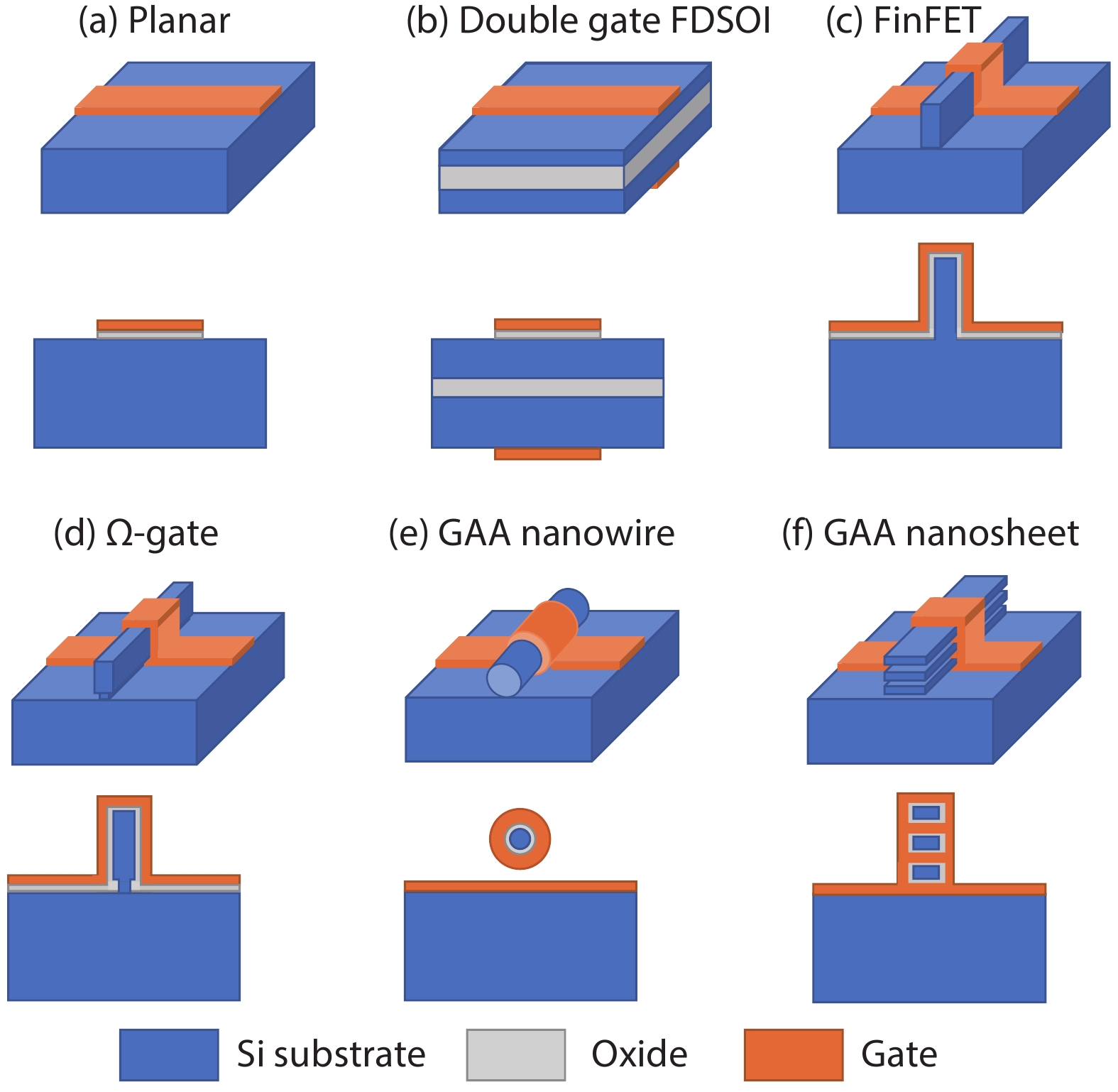
Fig. 2. (Color online) Evolution of MuGFETs from the planar device to the stacking structures. (a) Planar MOSFET. (b) Double-gate (DG) fully depleted SOI MOSFET. (c) FinFET. (d) Ω-gate MOSFET. (e) GAA NW MOSFET. (f) GAA multilayer nanosheet MOSFET.
Fig. 3. (Color online) DIBL performance as a function of gate length among FDSOI, FinFET and planar technologies[29 ].
Fig. 4. (Color online) Comparison of DIBL from ETSOI, DG, tri-gate, and GAA technologies as effective channel length reduces. Data are obtained from IBM and Intel Corp[30 , 31 ].
Fig. 5. (Color online) I ON–DIBL characteristics for MuGFETs with various technologies. As DIBL is a direct indicator of SCE suppression, devices with higher I ON and lower DIBL suggests a better electrostatic performance[11 , 17 –19 , 31 –39 ].
Fig. 6. (Color online) Thermal resistivity R th of Si fins for 14, 10 and 7 nm technology nodes as (a) the number of fins varies and (b) the fin height/aspect ratio changes[46 , 47 ].
Fig. 7. (Color online) Thermal conductivity for various materials used in gate stack, source/drain, channel, isolation and interconnects in a MuGFET. The conductivity reduces as the technology node shrinks. Higher mobility channel materials like Ge and SiGe also exhibit lower thermal conductivity[48 –52 ].
Fig. 8. I D–V G characteristics of a Si FinFET measured at drain voltage V D = 1.0 V illustrated in both logarithm (left) and linear (right) scales. The threshold voltage is taken by constant current method while I Dsat is taken as the drain current at V G = V Tsat + 1.0 V[24 ].
Fig. 9. (Color online) (a) The schematic illustration of a pulsed I –V testing system for a MOSFET. Pulsed signals are input at the gate electrode and sensed at the drain electrode while the source electrode is kept ground[24 , 25 ]. (b) The waveform of V G used for the I D–V G characterization. (c) I D–V G characteristics of a Si FinFET (L G = 80 nm) measured at V D = 1.0 V, using pulse measurement with various pulse widths[24 ].
Fig. 10. (a) Total resistance R Total = V D/I D at V D = 50 mV as a function of V G at various characterization temperature. The experimental data (dots) fits well with the resistance model (lines)[24 ]. (b) Corrected λ o/l o ratio for FinFETs at L G ranging from ~20 to ~150 nm, measured by both DC and pulsed I–V methods[24 ].
Fig. 11. A summary of 1/B sat as a function of L G for Si FinFETs, GeOI FETs and FDSOI/UTB FETs. Experimentally extracted B sat before and after R SD correction, with and without SHE are provided for comparison with the simulated curves[24 , 25 ].
Fig. 12. (Color online) The change of interface trap density ΔN it as the fin density and V D increase for bulk FinFETs. The stress time t stress is 1000 s[23 ].
Fig. 13. (Color online) Aging contribution from NBTI, PBTI, NHCD, and PHCD are compared for 14 and 10 nm technology nodes. Since the improvement in NBTI from 14 to 10 nm node could compensate the aggravation of HCD for both p- and n-FinFETs, the end-of-line (EOL) drive for the 10 nm node actually improves by 1.65 times[45 ].
Fig. 14. (Color online) Comparison of SS and I ON/I off ratio at various L G for MuGFETs with novel high-mobility channels[76 –83 ].

Set citation alerts for the article
Please enter your email address
© Copyright 2018-2021 | Chinese Laser Press. All Rights Reserved 沪ICP备15018463号-20