• Journal of Semiconductors
  • Vol. 42, Issue 2, 023102 (2021)
Ying Sun1, Xiao Yu2, Rui Zhang1, Bing Chen1, and Ran Cheng1
Author Affiliations
  • 1School of Micro-Nano Electronics, Zhejiang University, Hangzhou 310058, China
  • 2Intelligent Chip Research Center, Zhejiang Lab, Hangzhou 311121, China
  • show less
    DOI: 10.1088/1674-4926/42/2/023102 Cite this Article
    Ying Sun, Xiao Yu, Rui Zhang, Bing Chen, Ran Cheng. The past and future of multi-gate field-effect transistors: Process challenges and reliability issues[J]. Journal of Semiconductors, 2021, 42(2): 023102 Copy Citation Text show less

    Abstract

    This work reviews the state-of-the art multi-gate field-effect transistor (MuGFET) process technologies and compares the device performance and reliability characteristics of the MuGFETs with the planar Si CMOS devices. Owing to the 3D wrapped gate structure, MuGFETs can suppress the SCEs and improve the ON-current performance due to the volume inversion of the channel region. As the Si CMOS technology pioneers to sub-10 nm nodes, the process challenges in terms of lithography capability, process integration controversies, performance variability etc. were also discussed in this work. Due to the severe self-heating effect in the MuGFETs, the ballistic transport and reliability characteristics were investigated. Future alternatives for the current Si MuGFET technology were discussed at the end of the paper. More work needs to be done to realize novel high mobility channel MuGFETs with better performance and reliability.

    1. Introduction

    Since the first demonstration of Si metal–oxide–semiconductor field-effect transistors (MOSFETs) in 1960s[1], the number of transistors per die for IC chips have been increased by at least 6 orders[2]. The dimensional scaling of Si MOSFETs drastically improves the cost-performance efficiency. However, starting from 90 nm technology node, further scaling of Si transistors encounters great challenges, from the perspective of both Si process complexity and theoretical bottlenecks. To overcome the mobility degradation[3] and short channel effects (SCEs) due to the aggressive device scaling, strained engineering as well as high-κ metal gate (HKMG) technique[4] have been implemented in the CMOS fabrication process by the industry. For planar technology, further scaling of transistors is approaching its physical limits.

    To further boost the cost-performance efficiency following Moore’s law, transistors with novel-structures have been adopted to improve the power density per footprint, for sub-20 nm technology nodes. Multi-gate MOSFETs (MuGFETs), owing to the additional conducting channels at the sidewalls, exhibit superior electrostatic control as well as higher current density per area. Since 22 nm technology node, tri-gate Si MOSFETs have been adopted by Intel[5]. Afterwards, 3-dimensional (3D) multi-gate structure has been implemented by the mainstream world-leading foundries, demonstrating unreplaceable advantages in SCE control and switching characteristics.

    In fact, multi-gate transistors have been experimentally demonstrated and studied for a long time since 1980s. The history of double gate MOSFETs on silicon-on-insulator (SOI) substrate can be pursued to late 80s[6]. However, since the architecture for planar SOI MOSFETs with front and back gate is not suitable for back-end of line (BEOL) design, vertically in-parallel double gate structures has been realized on SOI MOSFETs, which is the early structural prototype for multi-gate MOSFET devices[7]. Later on, multi-gate transistors, namely, double-gate (DG) FinFET[8, 9], tri-gate FinFET[5, 10, 11], Ω-gate MOSFETs[12], segmented-gate (SG) MOSFETs[13], gate-all-around (GAA) MOSFETs[14, 15], 3D stacked nanowire (NW) MOSFETs[16-18], multilayer nanosheet MOSFETs[19], were immensely studied and massively demonstrated, especially after its compatibility with the conventional Si CMOS platform was demonstrated by UCBerkeley[8]. Excellent gate control and mobility improvement could be achieved by the realization of volume inversion especially for structures with more degree of gate wrapping and smaller cross-sectional channel area normal to the carrier transport direction. On the other hand, although the above-mentioned factors are beneficial to the SCE control and On-current ION enhancement for ultrascaled MOSFETs, these factors also lead to severe self-heating effect (SHE) due to the combinational effect of more heat generation (higher current density) and poorer heat dissipation (thinner channel)[20, 21]. The increased heat generated near the channel/drain boundary[22] would introduce various issues in terms of device performance and reliability[20], including accelerated bias-temperature instability (BTI)[23] and hot carrier injection (HCI) degradation[24, 25], deteriorate carrier transport characteristics etc.

    In this work, we will review the process development and reliability issues related to the state-of-the-art Si MuGFETs. From the historical perspective, the development of various MuGFET technologies will be clearly provided, followed by a discussion on the process challenges based on current technology. Next, the reliability issues, including SHE, carrier transport, BTI and HCI are discussed for various MuGFET technologies. Among the existing review works on MuGFETs, the carrier transport behavior of these ultrascaled 3D devices was rarely analyzed. In this paper, the ballistic transport characteristics of MuGFETs and the impact of SHE on it were thoroughly summarized for MuGFETs, thin body SOI FETs (w/ and w/o HCI), and thin body GeOI FET. The SHE induced transport and reliability issues, especially the difference with the planar transistors, will be discussed. An overlook of the future technology trend on new material MuGFETs will be touched up at the end.

    2. Process development of Si multi-gate transistors

    2.1. A historical view on the development of MuGFETs

    In late 1980s, double-gate Si MOSFETs was initially demonstrated on SOI substrate. The purpose of the back gate is to tune the threshold voltage VT of the front-gate transistor[
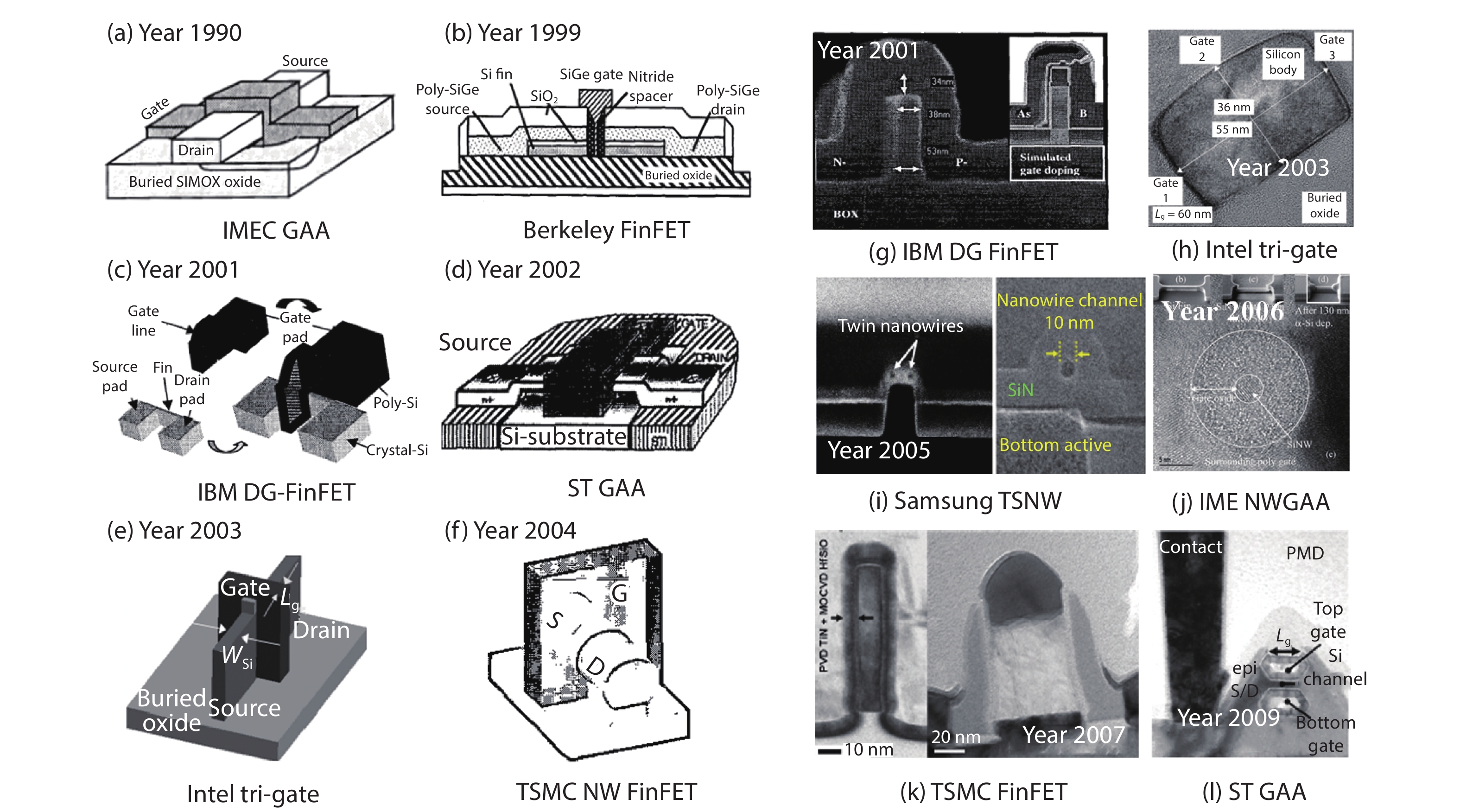
26]. Meanwhile, multi-gate transistors, like GAA MOSFETs and double-gate FinFET were demonstrated also on SOI substrate, as the insertion of buried oxide could eliminate the substrate leakage and simplify the process steps for fin-to-fin isolation. In 1999, Huang et al.[8] demonstrated the first FinFET with a gate length LG of sub-50 nm and a fin width of 15−30 nm. Following that, leading research groups and foundries like IBM[11], STMicroelectronics[15], Intel[5, 10], TSMC[16, 27], Samsung[17]. IME[18], etc. demonstrate their MuGFET technology with excellent control of SCEs and decent transfer characteristics. The schematics and cross-sectional TEM images of these devices are shown in Fig. 1. Fig. 2 summarizes the available structures for MuGFET that have been reported by several research groups including DG FDSOI FET [Fig. 2(b)], FinFET [Fig. 2(c)], Ω-gate FET [Fig. 2(d)], GAA NW FET [Fig. 2(e)], and GAA stacking nanosheet FET [Fig. 2(f)], in both 3D and cross-section views. As shown in the schematics, the sidewall channel offers extra dimension of conducting surfaces for carrier transport, therefore, the novel designed MuGFET structure could realize higher current per substrate area than the conventional planar transistors. For MuGFETs with thinner or narrower channel, volume inversion can be realized in the entire channel region, offering an improvement in carrier mobility as well as electrostatic control. Fig. 3 compare the drain-induced barrier lowering (DIBL) for transistors fabricated with different process technology, namely, bulk planar FETs, fully-depleted SOI (FDSOI) FETs, and FinFETs[29]. DIBL is closely related to the gate control over the channel region. A smaller DIBL indicates a good suppression of SCEs. For the three groups of devices in Fig. 3, at the same LG, DIBL is obviously lower for FinFETs, as compared with planar transistors. Furthermore, among FinFETs with various fin widths but the same LG, narrower fins lead to even lower DIBL, indicating that it is the cross-sectional area normal to the carrier transport direction determines the degree of gate control over the transistor channel. A smaller conducting area leads to a lower DIBL and better SCE control. The DIBL–LG/λ and DIBL–LG profiles were extracted for ETSOI, DG, tri-gate, and GAA FETs based on data from IBM and Intel Corp[30, 31], respectively. As shown in Fig. 4(b), as the degree of gate wrapping increases, smaller DIBL could be achieved at the same LG. As the mean-free path λ is longer for fully depleted and undoped channel, therefore, ETSOI FETs exhibit the longest λ. In Fig. 4(a), at the same LG/λ, the value of DIBL is similar for all the four technologies.

    (a–f) Schematics of MuGFETs with different gate geometries: (a) IMEC’s gate-all-around (GAA) MOSFET[14], (b) the world-first FinFET[8], (c) IBM’s double-gate (DG) FinFET[11], (d) STMicroelectronics’s GAA MOSFET[15], (e) Intel’s tri-gate FinFET[10], (f) TSMC’s nanowire FinFET[16]. (g–i) TEM images showing the cross-sectional view of fins/nanowires from early works: (g) IBM’s DG FinFET[11], (h) Intel’s tri-gate FinFET[10], (i) Samsung’s nanowire MOSFET[17], (j) IME’s nanowire GAA MOSFET[18], (k) TSMC’s FinFET[27], (l) STMicroelectronics’s GAA MOSFET[28].

    Figure 1.(a–f) Schematics of MuGFETs with different gate geometries: (a) IMEC’s gate-all-around (GAA) MOSFET[14], (b) the world-first FinFET[8], (c) IBM’s double-gate (DG) FinFET[11], (d) STMicroelectronics’s GAA MOSFET[15], (e) Intel’s tri-gate FinFET[10], (f) TSMC’s nanowire FinFET[16]. (g–i) TEM images showing the cross-sectional view of fins/nanowires from early works: (g) IBM’s DG FinFET[11], (h) Intel’s tri-gate FinFET[10], (i) Samsung’s nanowire MOSFET[17], (j) IME’s nanowire GAA MOSFET[18], (k) TSMC’s FinFET[27], (l) STMicroelectronics’s GAA MOSFET[28].

    (Color online) Evolution of MuGFETs from the planar device to the stacking structures. (a) Planar MOSFET. (b) Double-gate (DG) fully depleted SOI MOSFET. (c) FinFET. (d) Ω-gate MOSFET. (e) GAA NW MOSFET. (f) GAA multilayer nanosheet MOSFET.

    Figure 2.(Color online) Evolution of MuGFETs from the planar device to the stacking structures. (a) Planar MOSFET. (b) Double-gate (DG) fully depleted SOI MOSFET. (c) FinFET. (d) Ω-gate MOSFET. (e) GAA NW MOSFET. (f) GAA multilayer nanosheet MOSFET.

    (Color online) DIBL performance as a function of gate length among FDSOI, FinFET and planar technologies[29].

    Figure 3.(Color online) DIBL performance as a function of gate length among FDSOI, FinFET and planar technologies[29].

    (Color online) Comparison of DIBL from ETSOI, DG, tri-gate, and GAA technologies as effective channel length reduces. Data are obtained from IBM and Intel Corp[30, 31].

    Figure 4.(Color online) Comparison of DIBL from ETSOI, DG, tri-gate, and GAA technologies as effective channel length reduces. Data are obtained from IBM and Intel Corp[30, 31].

    The initial demonstration of MuGFET technology was realized on SOI platform due to the simplicity in process design and elimination of junction leakage to the substrate. In 2011, Intel announced its advanced 22 nm FinFET technology on bulk Si wafer[5], which promotes the adoption of bulk FinFET technology in the industry. Nowadays, mainstream foundries have chosen bulk Si FinFET structure for their most advanced technology nodes.

    2.2. Process challenges in state-of-the-art MuGFETs

    To achieve better gate control over SCEs, the narrow fin and ultrathin nanosheet structures are exploited in the most advanced MuGFETs. Fig. 5 provides the ION–DIBL data for several advanced Si MuGFETs reported in recent years with different process technologies[11, 17-19, 32-39]. At similar gate length, planar transistors (in black) exhibit much larger DIBL than the MuGFETs, indicating poor control of SCEs. Although FDSOI transistors could also be used for excellent SCE suppression, the current per footprint is lower than FinFETs[27, 37], and what’s more, the 3D stacked NS MuGFETs[19], as the latter two technologies utilize the advantage of vertical dimension for carrier transport.

    (Color online) ION–DIBL characteristics for MuGFETs with various technologies. As DIBL is a direct indicator of SCE suppression, devices with higher ION and lower DIBL suggests a better electrostatic performance[11, 17–19, 31–39].

    Figure 5.(Color online) ION–DIBL characteristics for MuGFETs with various technologies. As DIBL is a direct indicator of SCE suppression, devices with higher ION and lower DIBL suggests a better electrostatic performance[11, 1719, 3139].

    With the continuous scaling down of Si CMOS, the Si process technology encounters more challenges for the realization of higher density, higher performance, and higher reliability Si MuGFET CMOS. Take the 7-layer NS MOSFET in Ref. [19] as an example. The 3D stacking design could help to achieve extraordinary ION per footprint but greatly increase the process difficulty in gate stack formation and heating-related degradation issues in the channel. In general, the process challenge for massive production of high-quality Si MuGFETs lies in the following aspects: lithography capability, product integration, variability control, threshold voltage tuning, and strain engineering[40-44].

    Lithography. To overcome the optical limits of ArF 193 nm DUV lithography, liquid material was introduced to the optical system to increase the numerical aperture (NA) of the existing DUV lithography tool. As the critical dimension is inversely proportional to NA, this method could help to further push down the critical feature size based on the current lithography technology. However, increasing NA will degrade the depth of focus (DOF) as it is inversely proportional to NA2. To solve this problem, thinner photoresist (PR) should be used. Paradoxically, thin PR cannot withstand the etching of structures with high respect ratio which is necessary for high ION MuGFETs. Therefore, the design of new mask with novel materials that can satisfy the dilemma between selectivity and film thickness is an important topic that needs to be solved.

    Product integration. The gate pitch (GP) is defined as LG + Wcon + 2Wsp, where Wcon is the contact width and Wsp is the spacer width from gate-to-contact[45]. As the GP keeps shrinking, the space for epitaxial growth of S/D junctions decreases, leading to an increase in the S/D resistance RSD. For sub-20 nm MuGFETs, the increase in RSD will drag down the overall ON-current performance obviously. Although increasing the doping level in S/D junctions can reduce RSD, as long as it reaches the solubility limit (~1021 cm−3), further reduction of RSD due to dimension scaling will be extremely challenging. Other than GP scaling, the fin pitch scaling also introduces several integration problems like S/D epi shorts and mobility degradation due to the aggressive thinning of fin width[44].

    Strain engineering. Both GP scaling and fin pitch scaling will reduce the space for epitaxial raised S/D (RSD). For p-MuGFETs with SiGe RSD, the scaling will leads to the reduction of channel strain and ION since smaller volume of the SiGe is less effective to induce compressive strain in the channel.

    Threshold voltage tunning. For high aspect ratio MuGFETs, the fully depleted channel could not be used for threshold voltage tunning. The VT adjustment could only be realized by the careful work function tunning of metal gate electrode[41]. Mid-gap metal like TiN could be used for both p- and n-channel MuGFETs to obtain a medium VT. For the demand of low VT CMOS, replacement metal gate (RMG) recess process with additional cap layer in between the gate metal and the high-κ dielectric is the commonly used method. However, since the GP scaling will give more pressure to the LG shrinking for the consideration of better RSD, the RMG recess process for an ultrascaled gate stack is also extremely difficult.

    Variability control. The source of FinFET performance variability comes from a lot of aspects. For 7 nm technology node, the GP is 56 nm and the fin pitch is only 30 nm[45]. At this geometry level, any process dispersion in the process integration can cause great impact on the electrical performance fluctuation of the MuGFETs. The lithography and etch process may cause the appearance of line edge roughness (LER) for both fin and gate structures. The implantation, thin film deposition, polishing and thermal process for sub-20 nm MuGFET technology are also difficult to control the wafer-level variability at such a tight process tolerance level.

    3. Reliability issues of multi-gate transistors

    3.1. Self-heating effect and carrier transport analysis

    For short channel transistors, self-heating issues have become increasingly ineligible. As the drive current is inversely proportional to the gate length, the power density increases as the gate length shrinks. Furthermore, as compared with the traditional 2D/planar device architecture, 3D/FinFET structure exhibits more severe SHE[46, 47]. As shown in Fig. 6[46, 47], from 22 nm technology node to 7 nm node, the aspect ratio of MuGFETs keeps increasing. Provided the mobility of thin film Si does not change among these nodes, for devices with the same LG, ION per wire/fin width increases as the aspect ratio increases. Therefore, the power per planar area increases, leading to higher heat generation. On the other hand, the heating dissipation efficiency decreases drastically as the dimension of the fins pioneers to higher aspect ratio. It is known that the fin thermal resistivity Rth of a MuGFET is closely related to the number, density, width, and aspect ratio of fins[46-52]. Fig. 6 shows the change of Rth as the technology node decreases for MuGFETs with different number of fins and width of fins[47]. Fig. 7 provides the value of Rth for common gate stack materials in thin film form, including HfO2, TiN, and Si fins at different technology nodes[48-52]. The trend of MuGFETs scaling, namely, higher aspect ratio, denser fin arrangement, thinner gate oxide and metal, smaller contact, leads to much smaller thermal resistivity for the entire transistor. In addition to the effect of higher planar power density, the self-heating effect has become a bottleneck limiting the performance and reliability of the advanced MuGFETs.

    (Color online) Thermal resistivity Rth of Si fins for 14, 10 and 7 nm technology nodes as (a) the number of fins varies and (b) the fin height/aspect ratio changes[46, 47].

    Figure 6.(Color online) Thermal resistivity Rth of Si fins for 14, 10 and 7 nm technology nodes as (a) the number of fins varies and (b) the fin height/aspect ratio changes[46, 47].

    (Color online) Thermal conductivity for various materials used in gate stack, source/drain, channel, isolation and interconnects in a MuGFET. The conductivity reduces as the technology node shrinks. Higher mobility channel materials like Ge and SiGe also exhibit lower thermal conductivity[48–52].

    Figure 7.(Color online) Thermal conductivity for various materials used in gate stack, source/drain, channel, isolation and interconnects in a MuGFET. The conductivity reduces as the technology node shrinks. Higher mobility channel materials like Ge and SiGe also exhibit lower thermal conductivity[4852].

    The increased SHE occurring near the channel/drain boundary would introduce various issues in device performance and reliability[24, 25], including extra degradation in carrier transport characteristics, BTI, HCI, cyclic and device-to-device variation. Fig. 8 shows the transfer characteristics of an SOI FinFET at LG = 80 nm measured at various temperatures[24]. As illustrated, the performance parameters, namely, subthreshold swing (SS) and ION both degrade as the channel/chunk temperature increases. For a MuGFET working under DC bias, the stabilized channel temperature would be within the range of 353–393 K. According to Fig. 8, the expected degradation of Ion would be above 15%.

    ID–VG characteristics of a Si FinFET measured at drain voltage VD = 1.0 V illustrated in both logarithm (left) and linear (right) scales. The threshold voltage is taken by constant current method while IDsat is taken as the drain current at VG = VTsat + 1.0 V[24].

    Figure 8.IDVG characteristics of a Si FinFET measured at drain voltage VD = 1.0 V illustrated in both logarithm (left) and linear (right) scales. The threshold voltage is taken by constant current method while IDsat is taken as the drain current at VG = VTsat + 1.0 V[24].

    For sub-100 nm FinFETs operated in quasi-ballistic regime, the ballistic transport characteristics would be greatly affected by SHE, especially when using the DC measurement setups. While in “real” IC circuit operated with a frequency of a few tens of GHz, the device temperature is much lower and therefore the SHE is less severe than that under DC measurement[53]. Therefore, the traditional DC method may not accurately characterize the ballistic transport behavior of Si FinFETs. Several fast measurement approaches[24, 54, 55] were proposed to analyze the carrier transport characteristics without SHE. Cheng et al.[24, 25] carried out the fast measurement by applied an ultrafast (sub-100 ns) voltage pulse on the gate electrode and sensed the corresponding change of voltage drop on the drain electrode, as illustrated in Fig. 9(a). The total “turned-on” time for the transistor is determined by the pulse width applied to the gate. The shorter the pulse width, the less heat was generated in the transistor channel, and consequently, the less occurrence of phonon scattering encountered by the carriers. Fig. 9(c) compares the transfer characteristics (IDVG) of an SOI FinFET with LG = 80 nm and WFin = 20 nm measured at three different speeds[24]. As the pulse width reduced from 1 μs to 100 ns, the time for heat generation and spreading out was reduced by an order, leading to less phonon scattering and a gradual increase in the saturation drive current IDsat.

    (Color online) (a) The schematic illustration of a pulsed I–V testing system for a MOSFET. Pulsed signals are input at the gate electrode and sensed at the drain electrode while the source electrode is kept ground[24, 25]. (b) The waveform of VG used for the ID–VG characterization. (c) ID–VG characteristics of a Si FinFET (LG = 80 nm) measured at VD = 1.0 V, using pulse measurement with various pulse widths[24].

    Figure 9.(Color online) (a) The schematic illustration of a pulsed IV testing system for a MOSFET. Pulsed signals are input at the gate electrode and sensed at the drain electrode while the source electrode is kept ground[24, 25]. (b) The waveform of VG used for the IDVG characterization. (c) IDVG characteristics of a Si FinFET (LG = 80 nm) measured at VD = 1.0 V, using pulse measurement with various pulse widths[24].

    It should be noted here that, compared to the bulk FinFET, the SOI FinFET has even worse thermal dissipation capability with the insertion of buried oxide layer whose thermal conductivity is only around 1% of Si at the same thickness[21, 56]. Therefore, SOI FinFETs suffer more SHE than the bulk FinFETs since both the narrow fin width and thick buried oxide will retard the efficiency of heat dissipation. Therefore, although SOI substrate was chosen for MuGFETs demonstration for a long time, bulk technology was eventually chosen for the mass production of FinFET ICs by the industry, which can partially lessen the SHE-related problems.

    According to Lundstrom’s theory[57, 58], for transistors operated in quasi-ballistic regime, the drive current IDsat is related to the carrier transport parameters, namely, carrier injection velocity υinj and ballistic efficiency Bsat by IDsat = injBsat·Cox(VGVT), where Cox is the oxide capacitance, W is channel width, VG is the gate voltage, and VT is the threshold voltage. Following that, a temperature dependent I–V technique was developed and used to determine backscattering parameters of sub-100 nm devices[59, 60]. In the temperature dependent backscattering model, Bsat can be obtained from the near-equilibrium mean-free path λo and the critical distance lo over which the potential drops by kBT from the peak of the conduction band barrier. The ratio λo/lo can be extracted from the values of η and α using

     (1)

    where η and α are defined to be the slopes of VT shift ΔVT and ΔIDsat/IDsat with respective to temperature T, respectively. From the extracted λo/lo, Bsat can be calculated using

     (2)

     (3)

    where rsat is the carrier backscattering ratio, i.e. the fraction of injected carriers being scattering back from the channel. Furthermore, as compared with the bulk planar transistors, the series resistance for short-channel FinFETs is much larger due to the shrunk S/D regions[61-63]. Whereas, one assumption made in the backscattering model introduced in Section 2 is that the temperature dependence of the S/D series resistance RSD is negligible. It is necessary for large planar devices with channel and source/drain (S/D) region in similar dimensions. However, for FinFET with ultra-narrow fins connected directly to the S/D region with large volume, the temperature dependence of RSD cannot be ignored. This is due to the fact that the quantum contact resistance, which originates from the interface between the 3D S/D regions and the low dimensional quantum-wire of S/D-extension regions, is sensitive to temperature[64]. Therefore, the temperature dependence of RSD should be taken into consideration in the backscattering model for ultra-scaled FinFETs. A modified temperature dependent model was provided in Ref. [54] The temperature dependent coefficient β is defined as

     (4)

    where ΔRSD is the change of RSD as the channel temperature T changes. By correcting the effect of temperature-dependent RSD on the backscattering model, λo/lo could be extracted by the following modified equation:

     (5)

    while the correlation among λo/lo, rsat and Bsat remains unchanged.

    For multi-gate transistors, the parasitic resistance exhibits large variability. Therefore, to accurately exempt the effect of RSD on the backscattering parameters, RSD was extracted for individual device at every characterization temperature. Fig. 10 shows the RTotalVG plot for a FinFET with LG = 40 nm at three different characterization T. By fitting the data points in Fig. 10(a), RSD at each T could be taken at very high gate bias. As T increases, RSD gradually increases. For the FinFET in Fig. 10, RSD shows a linear relationship with T and its temperature dependent coefficient β is 0.591 Ω/K. Based on the corrected backscattering model, λo/lo was extracted at various gate lengths for both the “DC” and “pulse” cases. The RSD-corrected λo/lo as a function of LG is shown in Fig. 10. The values of λo/lo without considering the temperature-dependent RSD in the backscattering model is also included in Fig. 10 for comparison. As discussed before, since using pulsed I–V method could exempt the SHE on the characterization of ballistic transport, the mean free path in “pulse” case is larger than that in the “DC” case, as in the latter case the channel is heated up due to the severe SHE, leading to more scattering or shorter mean free path. As shown in Fig. 10, λo/lo ratio is higher for devices with shorter LG. As λo in the “pulse” case is larger, λo/lo ratio extracted from the pulsed I–V measurement is generally higher than the one extracted from the DC measurement. The difference of λo/lo between the two measurement conditions is slightly higher for FinFETs with smaller LG. As LG decreases, λo/lo in both “DC” and “pulse” cases increase while that extracted from pulsed I–V measurements increases more. This result indicates that self-heating may have more effects for devices with shorter LG. For sub-100 nm devices, using DC measurement to estimate the backscattering parameters may not cause large discrepancies but for FinFETs with sub-50 nm or even smaller gate length, pulsed I–V method would be more accurate for the extraction of backscattering parameters.

    (a) Total resistance RTotal = VD/ID at VD = 50 mV as a function of VG at various characterization temperature. The experimental data (dots) fits well with the resistance model (lines)[24]. (b) Corrected λo/lo ratio for FinFETs at LG ranging from ~20 to ~150 nm, measured by both DC and pulsed I–V methods[24].

    Figure 10.(a) Total resistance RTotal = VD/ID at VD = 50 mV as a function of VG at various characterization temperature. The experimental data (dots) fits well with the resistance model (lines)[24]. (b) Corrected λo/lo ratio for FinFETs at LG ranging from ~20 to ~150 nm, measured by both DC and pulsed I–V methods[24].

    Fig. 11 compares the ballisticity of FinFETs, FDSOI planar Si and Ge FETs. The trendline in the figure is obtained based on a numerical fitting model[24, 25]. A higher Bsat indicates a more temperature-independent carrier transport, or in other words, the performance of a transistor is more independent of the phonon scattering and mobility. According to the figure, FinFET technology exhibits superior ballisticity especially for those with improved S/D parasitic resistance and smaller gate length. From this perspective, improving the ballisticity of FinFETs could decrease the dependency of IDsat on the working temperature, and therefore mitigate the SHE on the device performance, which is quite severe in the 3D structured ultrascaled transistors.

    A summary of 1/Bsat as a function of LG for Si FinFETs, GeOI FETs and FDSOI/UTB FETs. Experimentally extracted Bsat before and after RSD correction, with and without SHE are provided for comparison with the simulated curves[24, 25].

    Figure 11.A summary of 1/Bsat as a function of LG for Si FinFETs, GeOI FETs and FDSOI/UTB FETs. Experimentally extracted Bsat before and after RSD correction, with and without SHE are provided for comparison with the simulated curves[24, 25].

    3.2. Bias temperature instability and hot carrier injection

    Biased temperature instability (BTI) and hot carrier degradation (HCD) are the two main factors determining the lifetime of a transistor. With the scaling down of conventional transistors, negative bias temperature instability (NBTI) has become a major aging issue for p-channel MOSFETs while positive bias temperature instability (PBTI) gets unobvious for n-channel transistors[65-67]. NBTI during device operation generates dangling bonds at the gate stack interface, causing a lot of charge trapping at the interface, and therefore, worsening the device performance, in terms of a threshold voltage shift (ΔVT), an increase in SS, a decrease in transconductance (gm) and ION etc. In addition, as mentioned in Section 3.1, SHE gets increasing prominent for 3D structured transistors with nanoscale dimensions. What’s worse, as SiGe raised source/drain (RSD) technique is commonly adopted in the p-channel device process by the industry, the lower Rth of SiGe (shown in Fig. 7) aggravates the SHE in the p-channel MuGFETs. Therefore, it could be anticipated that NBTI will be a dominant device aging factor in MuGFET CMOS circuits.

    For quite a period of time along the roadmap of Moore’s law, HCD is no longer an issue on the aging of CMOS[23]. However, as the device architecture evolutes to the more complicated 3D structures, HCD has re-appeared to be a crucial issue in both the n- ad p-channel MuGFETs. Again, owing to the more severe SHE in p-MuGFETs, the HCD of them is more significant than that of the n-MuGFETs, although the activation energy and the carrier effective mass are much higher for the former. Besides, as compared with the nanoscale planar transistors with negligible SHE, the heat generated in the MuGFET channel will elevate the lattice temperature. Therefore, although HCD occurs at high VD where the vertical field is much reduced, the SHE-induced high temperature will still result in obvious NBTI, making it difficult to differentiate the amount of contribution for device aging between HCD and NBTI for p-MuGFETs. Samsung studied[23] the impact of SHE on the change of interface trap density ΔNit as the fin density and VD vary for bulk FinFETs, as shown in Fig. 12. Increasing fin density will aggravate the SHE, therefore, speeding up the generation of Nit. As Nit will affect both BTI and HCD-induced ΔVT, it could be concluded that even at high VD where the vertical field is lessened, for devices suffering from severe SHE, NBTI still plays an important role in the total shift of threshold voltage, or in other words, the lifetime of MuGFETs.

    (Color online) The change of interface trap density ΔNit as the fin density and VD increase for bulk FinFETs. The stress time tstress is 1000 s[23].

    Figure 12.(Color online) The change of interface trap density ΔNit as the fin density and VD increase for bulk FinFETs. The stress time tstress is 1000 s[23].

    Fig. 13 summarizes the estimated aging contribution for HCD and BTI for both p- and n-channel FinFET from Intel, based on its 14 and 10 nm node FinFETs[45]. For both nodes, PBTI keeps negligible while the aging contribution from NBTI is reduced for 10 nm node. The general aggravation in reliability degradation from 14 to 10 nm node comes more from the HCD. With the existence of SHE, the portion of p-MuGFET HCD (PHCD) increases more than 2 times, while that for n-MuGFET HCD (NHCD) increases less.

    (Color online) Aging contribution from NBTI, PBTI, NHCD, and PHCD are compared for 14 and 10 nm technology nodes. Since the improvement in NBTI from 14 to 10 nm node could compensate the aggravation of HCD for both p- and n-FinFETs, the end-of-line (EOL) drive for the 10 nm node actually improves by 1.65 times[45].

    Figure 13.(Color online) Aging contribution from NBTI, PBTI, NHCD, and PHCD are compared for 14 and 10 nm technology nodes. Since the improvement in NBTI from 14 to 10 nm node could compensate the aggravation of HCD for both p- and n-FinFETs, the end-of-line (EOL) drive for the 10 nm node actually improves by 1.65 times[45].

    With the aggressive scaling down of MuGFETs, BTI and HCI are not the only reliability issues in the MuGFET technologies. Reliability topics like electromigration[68, 69], device-to-device variation[70, 71], cycle-to-cycle variation[70], random telegraph noise[72, 73], dielectric breakdown characteristics[74, 75] etc. are also get more severe. To improve the reliability and lifetime of MuGFETs, gate stack quality and device structures need to be optimized. For example, as also shown in Fig. 13, with higher annealing temperature, the defects in the gate stack from 14 to 10 nm are reduced, leading to an obvious reduction of NBTI for 10 nm node transistors. The great reduction in NBTI could cancel off the large increase of degradation from PHCD and NHCD, leading to an overall increase of the end-of-life (EOL) drive. However, increasing thermal budget leads to junction lateral movement, which degrades the HC lifetime as well as the gate oxide quality. The state-of-the art MuGFET technology, like novel contact material selection, self aligned contact-over-active-gate (COAG)[45, 66] and new isolation designs etc, helps to increase the packing density and device performance, but unavoidably degrades the transistor and circuit reliability. The aggressive gate pitch reduction also worsens the HCD and intrinsic gate dielectric breakdown. Therefore, more work on process co-optimization needs to be done to balance the trade-off among device performance, cost per function, and reliability.

    4. Future trends

    Although Si CMOS technology is still the sole choice for mass production of IC chips by the industry, in-depth research has been done to explore and pursue novel material transistors with higher-mobility beyond Si MOSFETs. III–V compound, Ge and GeSn channel MOSFETs were demonstrated to overcome the mobility limit of the traditional Si transistors[76-83]. Although these novel materials exhibit superior intrinsic mobility than Si, the interfaces of them with gate dielectrics are quite defective, leading to worse device performance and reliability, which hinders the replacement of current Si CMOS technology which these novel material technologies.

    To overcome the interface problems, in the past ten years, various passivation techniques were examined on the novel channel transistors[84-89]. For Ge MOSFETs, the interface passivation with ultrathin GeOx layer grown by plasma post oxidation method[88], quantum confined passivation layers (InAlP[85] or Si[86]), and high pressure passivation technique[87] etc, are demonstrated to sufficiently improved the mobility of Ge MOSFETs by either reducing the Nit, or confining the carrier transport away from the interface. Based on these effective passivation techniques, high performance SiGe, Ge, GeSn and III–V compound MuGFETs were fabricated, demonstrating excellent control of SCEs and On-current performance. Fig. 14 benchmarks the SS and ION/Ioff ratio for several high performance MuGFETs with novel channel materials[76-83]. The reliability issue of high mobility MuGFETs is another concern when considering their possibility to be the future generation of CMOS. It is reported the interface between SiGe and high-κ metal gate (HKMG) is better than either the Si/HKMG or Ge/HKMG interface[90], which enables the possible implementation of SiGe 3D CMOS with high performance and reliability for commercialized IC applications. For MuGFETs with other channel materials, interface engineering is still a very important technical challenge which needs to be solved in the future.

    (Color online) Comparison of SS and ION/Ioff ratio at various LG for MuGFETs with novel high-mobility channels[76–83].

    Figure 14.(Color online) Comparison of SS and ION/Ioff ratio at various LG for MuGFETs with novel high-mobility channels[7683].

    5. Conclusion

    3D structured MuGFETs with several different gate stack technologies were reviewed in this work. With more degree of gate wrapping over the transistor channel, excellent control of SCEs and volume inversion of channel can be achieved, demonstrating Si MuGFETs with superior electrostatic characteristics. For 14 nm technology node and beyond, the difficulties in process integration and co-optimization are discussed, as so to further improve the device performance and reliability. The carrier transport characteristics, BTI and HCI aging for Si MuGFETs with severe SHE were also investigated. At the end of the review, the possible future MuGFETs with novel high-mobility channels were discussed and compared. To make it possible to replace the current high performance Si MuGFETs, process optimization is still necessary to improve the gate stack quality and source/drain junctions.

    Acknowledgements

    The authors would like to express their deep gratitude to Prof. Hanming Wu from the School of Micro-nano Electronics, Zhejiang University for his valuable and inspiring discussion with the authors. This work was supported by Zhejiang Provincial Natural Science Foundation of China under Grant LR18F040001, LY19F040001, and the Opening Project of Key Laboratory of Microelectronic Devices & Integrated Technology, Institute of Microelectronics, Chinese Academy of Sciences.

    References

    [1] S R Hofstein, F P Heiman. The silicon insulated-gate field-effect transistor. Proc IEEE, 51, 1190(1963).

    [2] G Moore. Cramming more components onto integrated circuits. Electronics, 38, 114(1965).

    [3] S E Thompson, M Armstrong, C Auth et al. A 90-nm logic technology featuring strained-silicon. IEEE Trans Electron Devices, 51, 1790(2004).

    [4] K Mistry, C Allen, C Auth et al. A 45 nm logic technology with high-k metal gate transistors, strained silicon, 9 Cu interconnect layers, 193nm dry patterning, and 100% Pb-free packaging. IEEE International Electron Devices Meeting, 247(2007).

    [5] C Auth, C Allen, A Blattner et al. A 22 nm high performance and low-power CMOS technology featuring fully-depleted tri-gate transistors, self-aligned contacts and high density MIM capacitors. Symp VLSI Technol VLSIT, 131(2012).

    [6] F Balestra, S Cristoloveanu, M Benachir et al. Double-gate silicon-on-insulator transistor with volume inversion: A new device with greatly enhanced performance. IEEE Electron Device Lett, 8, 410(1987).

    [7]

    [8] X J Huang, W C Lee, C Kuo et al. Sub 50-nm FinFET: PMOS. IEEE International Electron Devices Meeting, 67(1999).

    [9] D Hisamoto, W C Lee, J Kedzierski et al. FinFET – a self-aligned double-gate MOSFET scalable to 20 nm. IEEE Trans Electron Devices, 47, 2320(2000).

    [10] B S Doyle, S Datta, M Doczy et al. High performance fully-depleted tri-gate CMOS transistors. IEEE Electron Device Lett, 24, 263(2003).

    [11]

    [12] F L Yang, H Y Chen, F C Chen et al. 25 nm CMOS Omega FETs. IEEE International Electron Devices Meeting, 255(2002).

    [13] B Ho, X Sun, N Xu et al. First demonstration of quasi-planar segmented-channel MOSFET design for improved scalability. IEEE Trans Electron Devices, 59, 2273(2012).

    [14] J P Colinge, M H Gao, A Romano-Rodriguez et al. Silicon-on-insulator ‘gate-all-around device’. International Technical Digest on Electron Devices, 595(1990).

    [15] S Monfray, T Skotnicki, Y Morand et al. 50 nm-gate all around (GAA)-silicon on nothing (SON)-devices: A simple way to co-integration of GAA transistors within bulk MOSFET process. Symposium on VLSI Technology, 108(2002).

    [16] F L Yang, D H Lee, H Y Chen et al. 5nm-gate nanowire FinFET. Symposium on VLSI Technology, 196(2004).

    [17] S D Suk, S Y Lee, S M Kim et al. High performance 5nm radius twin silicon nanowire MOSFET (TSNWFET): Fabrication on bulk Si wafer, characteristics, and reliability. IEEE International Electron Devices Meeting, 181(2005).

    [18] N Singh, A Agarwal, L K Bera et al. High-performance fully depleted silicon nanowire (diameter ≤ 5 nm) gate-all-around CMOS devices. IEEE Electron Device Lett, 27, 383(2006).

    [19] S Barraud, B Previtali, C Vizioz et al. 7-levels-stacked nanosheet GAA transistors for high performance computing. IEEE Symposium on VLSI Technology, 1(2020).

    [20]

    [21] E Pop. Energy dissipation and transport in nanoscale devices. Nano Res, 3, 147(2010).

    [22] L X Yin, L Shen, H Jiang et al. Impact of self-heating effects on nanoscale Ge p-channel FinFETs with Si substrate. Sci China Inf Sci, 61, 1(2017).

    [23] D Son, K Hong, H Shim et al. New insight into negative bias temperature instability degradation during self-heating in nanoscale bulk FinFETs. IEEE Electron Device Lett, 40, 1354(2019).

    [24] R Cheng, X Yu, B Chen et al. Investigation of self-heating effect on ballistic transport characterization for Si FinFETs featuring ultrafast pulsed IV technique. IEEE Trans Electron Devices, 64, 909(2017).

    [25] R Cheng, X Yu, B Chen et al. First investigation of hot carrier injection effects on ballistic transport characteristics for SOI MOSFETs featuring ultrafast pulsed IV measurement. International Reliability Physics Symposium (IRPS), 3E-3(2017).

    [26] H K Lim, J G Fossum. Threshold voltage of thin-film silicon-on-insulator (SOI) MOSFET's. IEEE Trans Electron Devices, 30, 1244(1983).

    [27] G Vellianitis, M J H van Dal, L Witters et al. Gatestacks for scalable high-performance FinFETs. IEEE International Electron Devices Meeting, 681(2007).

    [28] G Bidal, J L Huguenin, S Denorme et al. Gate-all-around technology: Taking advantage of ballistic transport. Proceedings of the European Solid State Device Research Conference, 315(2009).

    [29]

    [30]

    [31] B Doris, Y H Kim, B P Linder et al. High performance FDSOI CMOS technology with metal gate and high-k. Symposium on VLSI Technology, 214(2005).

    [32] K Mistry, C Allen, C Auth et al. A 45 nm logic technology with high-k metal gate transistors, strained silicon, 9 Cu interconnect layers, 193nm dry patterning, and 100% Pb-free packaging. IEEE International Electron Devices Meeting, 247(2007).

    [33] C H Diaz, K Goto, H T Huang et al. 32nm gate-first high-k/metal-gate technology for high performance low power applications. IEEE International Electron Devices Meeting, 1(2008).

    [34] R Coquand, S Monfray, S Barraud et al. Innovative through-Si 3D lithography for ultimate self-aligned planar double-gate and gate-all-around nanowire transistors. Symposium on VLSI Technology, T226(2013).

    [35]

    [36] S Barraud, R Coquand, M Casse et al. Performance of omega-shaped-gate silicon nanowire MOSFET with diameter down to 8 nm. IEEE Electron Device Lett, 33, 1526(2012).

    [37] C Auth, C Allen, A Blattner et al. A 22 nm high performance and low-power CMOS technology featuring fully-depleted tri-gate transistors, self-aligned contacts and high density MIM capacitors. Symposium on VLSI Technology (VLSIT), 131(2012).

    [38] N Loubet, T Hook, P Montanini et al. Stacked nanosheet gate-all-around transistor to enable scaling beyond FinFET. Symposium on VLSI Technology, T230(2017).

    [39]

    [40]

    [41] M Xu, H X Yin, H L Zhu et al. Device parameter optimization for sub-20 nm node HK/MG-last bulk FinFETs. J Semicond, 36, 044007(2015).

    [42] S Deleonibus. Ultra-thin films and multigate devices architectures for future CMOS scaling. Sci China Inf Sci, 54, 990(2011).

    [43] M Jurczak, N Collaert, A Veloso et al. Review of FINFET technology. IEEE International SOI Conference, 1(2009).

    [44] A Malinowski, J Chen, S K Mishra et al. What is killing Moore's Law, challenges in advanced FinFET technology integration. MIXDES - 26th International Conference Mixed Design of Integrated Circuits and Systems, 46(2019).

    [45]

    [46] V Moroz. Technology inflection points: Planar to FinFET to nanowire. Int Symp Phys Design(2016).

    [47]

    [48] Z Aksamija, I Knezevic. Thermal conductivity of Si1–xGex/Si1–yGey superlattices: Competition between interfacial and internal scattering. Phys Rev B, 88, 155318(2013).

    [49] E Bury, B Kaczer, J Mitard et al. Characterization of self-heating in high-mobility Ge FinFET pMOS devices. IEEE Symp VLSI Technol VLSI Technol, T60(2015).

    [50] E Pop, S Sinha, K E Goodson. Heat generation and transport in nanometer-scale transistors. Proc IEEE, 94, 1587(2006).

    [51] Y Terada, K Ohkubo, T Mohri et al. Thermal conductivity of cobalt-base alloys. Metall Mater Trans A, 34, 2026(2003).

    [52] Y Zhao, Y M Qu. Impact of self-heating effect on transistor characterization and reliability issues in sub-10 nm technology nodes. IEEE J Electron Devices Soc, 7, 829(2019).

    [53] W C Chen, R Cheng, D W Wang et al. Electrothermal effects on hot-carrier reliability in SOI MOSFETs—AC versus circuit-speed random stress. IEEE Trans Electron Devices, 63, 3669(2016).

    [54] R S Wang, J Zhuge, C Z Liu et al. Experimental study on quasi-ballistic transport in silicon nanowire transistors and the impact of self-heating effects. IEEE International Electron Devices Meeting, 1(2008).

    [55] H Jiang, X Y Liu, N Xu et al. Investigation of self-heating effect on hot carrier degradation in multiple-fin SOI FinFETs. IEEE Electron Device Lett, 36, 1258(2015).

    [56] T Yamane, N Nagai, S I Katayama et al. Measurement of thermal conductivity of silicon dioxide thin films using a 3ω method. J Appl Phys, 91, 9772(2002).

    [57] M Lundstrom. Elementary scattering theory of the Si MOSFET. IEEE Electron Device Lett, 18, 361(1997).

    [58] M S Lundstrom. On the mobility versus drain current relation for a nanoscale MOSFET. IEEE Electron Device Lett, 22, 293(2001).

    [59] M J Chen, H T Huang, K C Huang et al. Temperature dependent channel backscattering coefficients in nanoscale MOSFETs. IEEE International Electron Devices Meeting, 39(2002).

    [60] T Y Liow, K M Tan, H C Chin et al. Carrier transport characteristics of sub-30 nm strained N-channel FinFETs featuring silicon-carbon source/drain regions and methods for further performance enhancement. IEEE International Electron Devices Meeting, 1(2006).

    [61] A Dixit, A Kottantharayil, N Collaert et al. Analysis of the parasitic S/D resistance in multiple-gate FETs. IEEE Trans Electron Devices, 52, 1132(2005).

    [62] R Tomita, H Kimura, M Yasuda et al. Improvement on sheet resistance uniformity of nickel silicide by optimization of silicidation conditions. Microelectron Reliab, 53, 665(2013).

    [63] T Matsukawa, Y X Liu, K Endo et al. Variability origins of parasitic resistance in FinFETs with silicided source/drain. IEEE Electron Device Lett, 33, 474(2012).

    [64] P H Su, Y M Li. Determination of source-and-drain series resistance in 16-nm-gate FinFET devices. IEEE Trans Electron Devices, 62, 1663(2015).

    [65] N Choudhury, U Sharma, H M Zhou et al. Analysis of BTI, SHE induced BTI and HCD under full VG/VD space in GAA nano-sheet N and P FETs. IEEE International Reliability Physics Symposium (IRPS), 1(2020).

    [66] C Prasad. A review of self-heating effects in advanced CMOS technologies. IEEE Trans Electron Devices, 66, 4546(2019).

    [67] M M Wang, J Y Zhang, H M Zhou et al. Bias temperature instability reliability in stacked gate-all-around nanosheet transistor. IEEE International Reliability Physics Symposium (IRPS), 1(2019).

    [68]

    [69] R Zhang, K X Yang, T Z Liu et al. New electromigration model and its potential application on degradation simulation for FinFET SRAM. International Integrated Reliability Workshop (IIRW), 1(2018).

    [70]

    [71] W K Wu, X An, X B Jiang et al. Line-edge roughness induced single event transient variation in SOI FinFETs. J Semicond, 36, 114001(2015).

    [72] J Z Chen, Y Nakasaki, Y Mitani. Deep insight into process-induced pre-existing traps and PBTI stress-induced trap generations in high-k gate dielectrics through systematic RTN characterizations and ab initio calculations. IEEE Symposium on VLSI Technology, 1(2016).

    [73] X P Zhan, Y F Xi, Q W Wang et al. Dual-point technique for multi-trap RTN signal extraction. IEEE Access, 8, 88141(2020).

    [74]

    [75] P C Feijoo, T Kauerauf, M Toledano-Luque et al. Time-dependent dielectric breakdown on subnanometer EOT nMOS FinFETs. IEEE Trans Device Mater Reliab, 12, 166(2012).

    [76] D Lei, K H Lee, S Y Bao et al. The first GeSn FinFET on a novel GeSnOI substrate achieving lowest S of 79 mV/decade and record high Gm, int of 807 μS/μm for GeSn P-FETs. Symposium on VLSI Technology, T198(2017).

    [77]

    [78]

    [79]

    [80]

    [81]

    [82] C L Chu, K Wu, G L Luo et al. Stacked Ge-nanosheet GAAFETs fabricated by Ge/Si multilayer epitaxy. IEEE Electron Device Lett, 39, 1133(2018).

    [83] W W Fang, N Singh, L K Bera et al. Vertically stacked SiGe nanowire array channel CMOS transistors. IEEE Electron Device Lett, 28, 211(2007).

    [84] X Gong, G Q Han, F Bai et al. Germanium–tin (GeSn) p-channel MOSFETs fabricated on (100) and (111) surface orientations with sub-400 °C Si2H6 passivation. IEEE Electron Device Lett, 34, 339(2013).

    [85]

    [86] B Liu, X Gong, G Q Han et al. High-performance germanium ω-gate MuGFET with Schottky-barrier nickel germanide source/drain and low-temperature disilane-passivated gate stack. IEEE Electron Device Lett, 33, 1336(2012).

    [87]

    [88] R Zhang, T Iwasaki, N Taoka et al. Al2O3/GeOx/Ge gate stacks with low interface trap density fabricated by electron cyclotron resonance plasma postoxidation. Appl Phys Lett, 98, 112902(2011).

    [89] J Mitard, C Shea, B DeJaeger et al. Impact of EOT scaling down to 0.85 nm on 70 nm Ge-pFETs technology with STI. VLSI Symp Tech Dig, 82(2009).

    [90] J Franco, B Kaczer, J Mitard et al. NBTI reliability of SiGe and Ge channel pMOSFETs with SiO2/HfO2 dielectric stack. IEEE Trans Device Mater Reliab, 13, 497(2013).

    Ying Sun, Xiao Yu, Rui Zhang, Bing Chen, Ran Cheng. The past and future of multi-gate field-effect transistors: Process challenges and reliability issues[J]. Journal of Semiconductors, 2021, 42(2): 023102
    Download Citation