• Journal of Semiconductors
  • Vol. 41, Issue 3, 032102 (2020)
Lin Luo, Jun Liu, Guofang Wang, and Yuxing Wu
Author Affiliations
  • Key Laboratory of RF Circuits and Systems, Ministry of Education, Hangzhou Dianzi University, Hangzhou 310018, China
  • show less
    DOI: 10.1088/1674-4926/41/3/032102 Cite this Article
    Lin Luo, Jun Liu, Guofang Wang, Yuxing Wu. Small-signal modeling and parameter extraction method for a multigate GaAs pHEMT switch[J]. Journal of Semiconductors, 2020, 41(3): 032102 Copy Citation Text show less
    Cross-sectional structure of the dual-gate GaAs pHEMT switch.
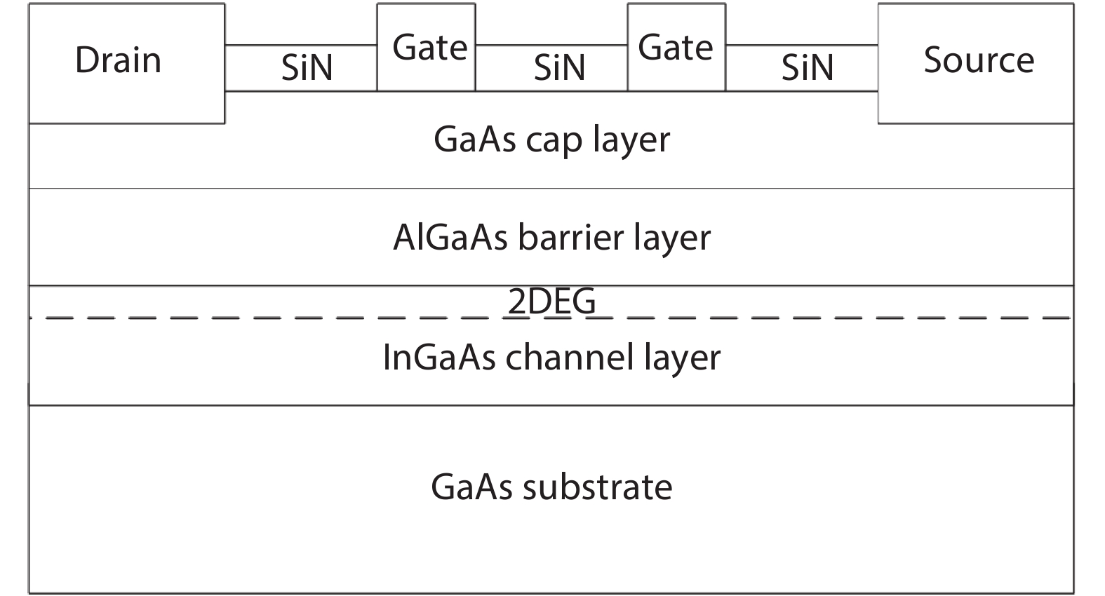
    Fig. 1. Cross-sectional structure of the dual-gate GaAs pHEMT switch.
    (Color online) Layout of the dual-gate GaAs pHEMT switch(125 μm × 5).
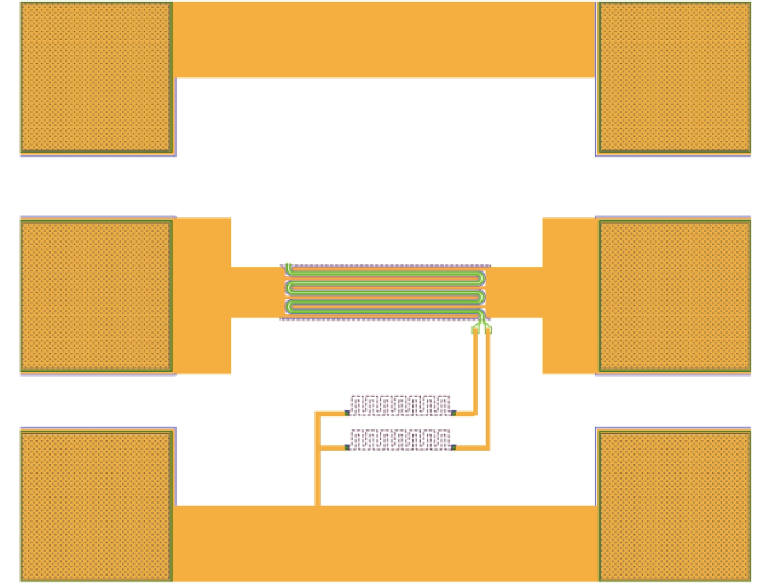
    Fig. 2. (Color online) Layout of the dual-gate GaAs pHEMT switch(125 μm × 5).
    Small-signal equivalent circuit of the dual-gate GaAs pHEMT switch.
    Fig. 3. Small-signal equivalent circuit of the dual-gate GaAs pHEMT switch.
    (Color online) Extracted parasitic capacitances versus frequency.
    Fig. 4. (Color online) Extracted parasitic capacitances versus frequency.
    Equivalent circuit of the GaAs pHEMT switch under the condition (Vds = 0 V, Vgs = 0 V).
    Fig. 5. Equivalent circuit of the GaAs pHEMT switch under the condition (Vds = 0 V, Vgs = 0 V).
    (Color online) Extracted parasitic inductors versus frequency.
    Fig. 6. (Color online) Extracted parasitic inductors versus frequency.
    The intrinsic part with RG, which blocks the RF signal.
    Fig. 7. The intrinsic part with RG, which blocks the RF signal.
    (Color online) Intrinsic capacitances versus frequency for the common-gate GaAs HEMT without RG.
    Fig. 8. (Color online) Intrinsic capacitances versus frequency for the common-gate GaAs HEMT without RG.
    Equivalent circuits of the dual-gate GaAs pHEMT switch.
    Fig. 9. Equivalent circuits of the dual-gate GaAs pHEMT switch.
    (Color online) Comparison of the S-parameters between the simulation (-) and measurement (◇) over a frequency range of 0.1–20 GHz for a device with size of 5 × 125 μm: (a) dual-gate off state, (b) dual-gate on state, (c) triple-gate off state, (d) triple-gate on state, (e) quadruple-gate off state, and (f) quadruple-gate on state.
    Fig. 10. (Color online) Comparison of the S-parameters between the simulation (-) and measurement (◇) over a frequency range of 0.1–20 GHz for a device with size of 5 × 125 μm: (a) dual-gate off state, (b) dual-gate on state, (c) triple-gate off state, (d) triple-gate on state, (e) quadruple-gate off state, and (f) quadruple-gate on state.
    (Color online) Illustration of the simulated and measured insertion loss and isolation (0.1–20 GHz) for a device with a size of 5 × 125 μm. (a) Insertion loss (dual-gate off state). (b) Isolation (dual-gate off state). (c) Insertion loss (triple-gate on state). (d) Isolation (triple-gate off state). (e) Insertion loss (quadruple-gate on state). (f) Isolation (quadruple-gate off state).
    Fig. 11. (Color online) Illustration of the simulated and measured insertion loss and isolation (0.1–20 GHz) for a device with a size of 5 × 125 μm. (a) Insertion loss (dual-gate off state). (b) Isolation (dual-gate off state). (c) Insertion loss (triple-gate on state). (d) Isolation (triple-gate off state). (e) Insertion loss (quadruple-gate on state). (f) Isolation (quadruple-gate off state).
    StateCgdCgsCdsCgg*Rds
    On state1.5 pF1.5 pF20.1 fF74.2 fF4.5 Ω
    Off state145 fF137 fF20.1 fF64 fF96 kΩ
    Table 1. Intrinsic elements of the GaAs HEMT switch with a gate size of 5 × 125 µm.
    GateDualTripleQuadruple
    Cds(on) (fF) 20.115.2111
    Cgs(on) (pF) 1.52.122.82
    Cgd(on) (pF) 1.52.152.73
    Rds(on) (Ω) 4.55.767
    Cds(off) (fF) 20.115.2111
    Cgs(off) (fF) 137144152
    Cgd(off) (fF) 145148161
    Rds(off) (kΩ) 96182160
    Cgg*(off) (fF) 6476.27121.6
    Table 2. Intrinsic parameters of GaAs HEMT switches with different gates.
    GateDualTripleQuadruple
    S11(off) 0.75860.9091.131
    S12(off) 2.5192.2941.981
    S21(off) 2.4122.3782.066
    S22(off) 1.3622.5181.746
    S11(on) 2.2572.4772.197
    S12(on) 1.1572.2852.805
    S21(on) 0.76940.60540.604
    S22(on) 2.29241.2010.573
    Table 3. The error percentage of GaAs HEMT switches with different gates.
    Lin Luo, Jun Liu, Guofang Wang, Yuxing Wu. Small-signal modeling and parameter extraction method for a multigate GaAs pHEMT switch[J]. Journal of Semiconductors, 2020, 41(3): 032102
    Download Citation